國立交通大學
電子工程學系 電子研究所碩士班
碩 士 論 文
降低金屬與N型鍺接觸電阻之研究
A Study on the Contact Resistance Reduction in
Metal/n-type Germanium Contacts
研究生:高銘鴻
指導教授:崔秉鉞 教授
降低金屬與N型鍺接觸電阻之研究
A Study on the Contact Resistance Reduction in
Metal/n-type Germanium Contacts
研究生:高銘鴻 Student : Ming-Hong Kao
指導教授:崔秉鉞 Advisor : Bing-Yue Tsui
國立交通大學 電子工程學系 電子研究所
碩士論文
A thesis
Submitted to Department of Electronics Engineering & Institute of Electronics College of Electrical Engineering and Computer Science
National Chiao Tung University in Partial Fulfillment of the Requirement
for the Degree of Master in
Electronic Engineering 2012
Hsinchu, Taiwan, Republic of China
i
降低金屬與N型鍺接觸電阻之研究
研究生:高銘鴻 指導教授:崔秉鉞
國立交通大學電子工程系 電子研究所碩士班
摘要
隨著製程技術的發展,使用矽做為主要半導體材料的金氧半場效電晶體不斷 地成功微縮,但是如果繼續發展下去很快的會碰到了物理極限的限制而導致無法 繼續提升性能。許多方式被提出來解決這個問題,鍺由於其較高的載子遷移率以 及與矽製程較大的相容性,被視為是下個世代中有機會取代矽做為通道的半導體 材料。但是N型鍺與金屬接面會有較大的蕭基位能障而導致較大的接觸阻抗,所 以如果我們要使用鍺做為金氧半場效電晶體的材料,降低N型鍺與金屬接觸阻抗 是必要的。本論文探討兩種不同的方式來降低N型鍺與金屬的接觸阻抗,分別是 以調變蕭基位能障的介電層插入元件與增加接面載子濃度的修正蕭基位障元件。 介電層插入製程已有文獻發表,前人研究使用三氧化二鋁以及二氧化鈦做為 介電層,由於二氧化鈦與鍺有較低的導帶差,因而在降低蕭基位能障之外還能達 到較小的穿隧阻抗,以致於有較大的導通電流,但是實際改善機制尚無定論。本 論文首先觀察到蕭基位能障鎖定效應在不同厚度的二氧化鈦介電層插入元件上 並沒有太大差異,所以推斷介電層插入元件是以改變鎖定位置為主的方式調變蕭 基位能障。再利用金氧半電容結構計算出介電層內部的固定電荷量並不足以造成 如此大的調變幅度,所以推論其調變方式是主要以接面因不同極性而產生的感應 偶極電荷為主。除此之外,我們發現介電層插入元件在攝氏300度經30分鐘的退 火條件下,特性就會變差且蕭基位能障會回升,退火溫度愈高,蕭基位能障愈高。 根據微結構分析,我們推論介電層因退火而產生的結晶化是導致特性變差的主要 原因,由於介電常數因結晶化而增加,介電層電容值增加所以電壓改變量較小,ii 導致蕭基位能障增加。較厚的二氧化鈦介電層會有較低的電容值,可能也是其蕭 基位能障較低的原因。 修正蕭基位障元件因為離子植入在金屬鍺化物而不是直接植入鍺基板,鍺基 板中產生的缺陷較少,所以之後退火時雜質就不會因為與缺陷的反應而提升雜質 擴散速率,進而在金屬與半導體的接面產生較淺且載子濃度較高的摻雜層。研究 發現提升活化溫度能得到更高的載子活化濃度,但是鎳化鍺的熱穩定性不佳,限 制了活化溫度在攝氏500度。為了增進鎳化鍺的熱穩定性,本論文提出在鎳與鍺 中間插入一層矽再讓其反應的技術,研究發現加入矽之後,鎳化鍺的熱穩定性從 500度提升到了550度,且具有較低的片電阻值。藉由使用摻雜矽的鎳化鍺來製做 修正蕭基位障元件,將活化溫度提升到550度,得到了更高的活化濃度。與傳統 直接植入鍺基板再退火的元件相比,修正蕭基位障元件具有較佳的活化濃度與較 淺的高濃度區域,因此修正蕭基位障接面具有當做短通道鍺基板金氧半場效電晶 體的源極與汲極的潛力。 本論文提出插入介電層以降低蕭基位能障高度的物理機制,並解釋了厚度與 退火溫度的效應,並提出新的修正蕭基位障技術,以降低接觸電阻,並得到高濃 度的淺接面,對於提升N型鍺的金氧半場效電晶體,極具應用潛力。
iii
A Study on the Contact Resistance Reduction in
Metal/n-type Ge Contacts
Student: Ming-Hong Kao Advisor: Bing-Yue Tsui
Department of Electronics Engineering
Institute of Electronics
National Chiao Tung University
Abstract
With the rapid progress of nano-fabrication technology, Si based MOSFETs have been successfully scaled down to 20 nm regime. However, the continued scaling will be a problem due to several physical and technical limitations, and the device performance may not be improved by further scaling down. Many methods have been purposed to solve this problem, because of the higher carrier mobilities and better process compatibility, Ge is considered a potential candidate to replace silicon as the next generation channel material. However, the contact resistance between metal and n-type Ge is very high due to the high Schottky barrier height. To implement high performance Ge NMOSFETs, reducing the contact resistance of metal/n-type Ge is critical.
In this thesis, two different methods to reduce the contact resistance of metal/n-type Ge are investigated. One is inserted dielectric-inserted junction and the other is modified Schottky barrier junction. The former is to modulate the Schottky barrier height and the latter is to enhance the doping concentration at the metal/Ge interface.
iv
The dielectric insertion method has been reported in literature. Both Al2O3 and
TiO2 have been used as the inserted dielectric layer. Because of the lower conduction
band offset of TiO2 to Ge, it can not only reduce the Schottky barrier height but also
achieve low tunneling resistance and high conduction current. However, the mechanism has not been well understood. In this thesis, we first observed that the Fermi level pinning effect is a very weak function of the TiO2 thickness so we infer
that the Schottky barrier height reduction by the dielectric insertion is due to the change of the pinning position. The amount of fixed charges in the thin dielectric layer is extracted from a MIS structure and it is found that the small amount of fixed charges is not sufficient to produce such a pronounced voltage drop to modulate the Schottky barrier height. It is thus recommended that the mechanism of the dielectric insertion method mainly comes from interface dipoles. Besides, it is observed that after annealing at 300 °C for 30 minutes, the Schottky barrier height will increase. The increase of the Schottky barrier height increase with the increasing of the annealing temperature. According to the microstructural analysis, it is postulated that the crystallization of the dielectric layer after annealing is the main reason for the increase of Schottky barrier height. Due to the dielectric constant increase after crystallization, the capacitance of the dielectric capacitor increases and causes smaller voltage drop so that the Schottky barrier height increases. The thicker TiO2 dielectric
layer has smaller capacitance, which might be the reason for the lower Schottky barrier height.
In the modified Schottky barrier method, dopants are implanted into metal-germanide instead of Ge so that the number of defects formed in substrate could be negligible, which would mitigate the dopants diffusion caused by the interaction between defects and dopants. A thin and high doping concentration layer can be formed at the metal/semiconductor interface. Increasing the activation
v
temperature will achieve higher doping concentration. But the allowed annealing temperature is limited by the poor thermal stability of NiGe films. To improve the thermal stability of NiGe films, a Si layer is inserted between Ni and Ge before annealing. The result shows that the thermal stability of NiGe film is improved by this Si-insertion layer from 500 °C to 550 °C. Using the Si-insertion technique, the activation temperature of MSB junctions can be raised to 550 °C so that the doping concentration is enhanced. Compared to the conventional junction with direct implantation into Ge, the junction depth is much shallower and the carrier concentration is much higher for the MSB junction which suggests that the MSB process is attractive for the short channel Ge MOSFETs.
In summary, this thesis proposed the mechanism of the Schottky barrier height modulation by dielectric insertion. The thickness effect and annealing effect are also explained. A new method, modified Schottky barrier method, is propsed to reduce the contact resistance between metal and n-type Ge by forming a thin and high concentration layer at the metal/Ge interface. This method is very promising for short channel Ge NMOSFET.
vi
致謝
能夠順利完成這篇論文,首先最感謝的是我的指導教授 崔秉鉞老師,從大 學做專題開始就在老師指導下做研究,在老師的熱心教導下,無論是在課業上或 是實驗上都直接給了很大的幫助。另外在做人處事方面,老師正直的性格與豐富 的人生經驗更是讓我學到了許多課外以外的重要道理。 實驗方面則感謝交大奈米中心與國家奈米元件實驗室所提供的製程機台。謝 謝實驗室的大家,特別感謝嶸健學長在實驗製程、結果討論上都幫助我很多,還 幫忙我做了許多複雜的實驗。也很感謝培宇學長、元宏學長跟子瑜經常與我討論 許多實驗上的東西,讓我可以更快的了解一些問題並且有辦法解決。感謝克勤不 厭其煩的幫我做需要花長時間的實驗,有時甚至做到快十二點才離開。感謝茂元 會與我討論一些寫論文的心得,使我在完成論文的過程中有聊天與討論的對象。 感謝炫滋幫我長爐管。感謝銘鴻、泰源經常陪我去吃飯聊天。感謝哲儒,在我忙 碌於其它實驗抽不出空時能替我分擔一些。感謝實驗室的大家,做實驗之餘一起 互相幫助勉勵,使我這兩年過得非常充實。 再來要感謝我的朋友,在我因實驗遇到問題而低潮時,能陪我聊天並給我支 持鼓勵,使我能更快的振作起來。最後要感謝我的家人,時常打電話關心問候, 讓我覺得很溫暖並且解決了我許多生活上的困難,謝謝你們。vii
Contents
Abstract (Chinese) i
Abstract (English) iii
Acknowledgements vi
List of Tables ix
List of Figures x
Chapter 1 Introduction ………..…...1
1-1 Why Studying Germanium………..1
1-2 Contact Resistance and Fermi Level Pinning in Germanium………...…...2
1-2-1 Schottky Barrier Formation………3
1-2-2 Contact Resistance………...4
1-2-3 Fermi-Level Pinning………...4
1-3 Methods for Fermi Level Depinning………..………...6
1-4 Germanium Metal Contact………..……….. ..7
1-4-1 Metal Germanide………7 1-4-2 Dopant Activation………...8 1-5 Motivation………9 1-6 Thesis Organization………10
Chapter 2 Experiments...……….………..………..14
2-1 Device Fabrication……….……...………...142-1-1 Dielectric Insertion Layer Junctions……….14
viii
2-2 Material Analysis and Electrical Measurement…………..…………..……….17
Chapter 3 Dielectric Insertion Junctions………...……....23
3-1 Introduction of Dielectric Insertion Method………...…...23
3-2 Currents of the two Dielectric Insertion Junctions – Al2O3 & TiO2………...23
3-3 Fermi Level Pinning Effect of TiO2 Dielectric Insertion Junctions…….…...25
3-4 Annealing Effect of Dielectric Insertion Junctions………....26
3-5 Summary of Dielectric Insertion Junctions………....……29
Chapter 4 Germaium MSB Junctions………..44
4-1 Introduction of Germanium MSB Junctions……….…..………...45
4-2 Activation of NiGe MSB Junctions………...45
4-3 Thermal Stability of NiGe after MSB Formation………..………47
4-4 Thermal Stability Improvement by Inserting a Si Film…………...…………..48
4-5 Dopant Diffusion and Activation of MSB Junctions………..…………...….49
4-6 Summaries of MSB Junctions………...……….50
Chapter 5 Summary and Future Works………...………...63
4-1 Summary………..……….….63
4-2 Future Works………..………...65
References………...………...68
ix
List of Tables
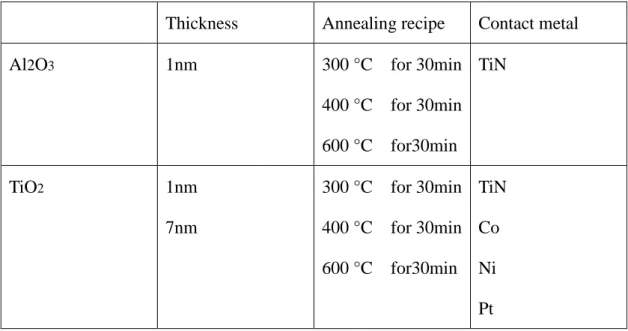
Chapter 2
Table 2-1 The main process recipes of depinning layer junction samples.…………..19 Table 2-2 The annealing conditions of MSB junction samples………19
x
List of Figures
Chapter 1
Fig.1-1 Formation of the Schottky barrier as metal approaches semiconductor surface[8].……….11 Fig.1-2 Schematic illustration of Fermi level pinning of a semiconductor surface with non-uniformly distributed surface states[9]………...……...….12 Fig.1-3 Band diagrams of Al2O3/Ge and TiO2/Ge structure [20]……….13
Chapter 2
Fig. 2-1 The process flow of depinning layer junction fabrication….……….20 Fig. 2-2 The process flow of MSB junction fabrication.……….….21
Chapter 3
Fig. 3-1 I-V characteristics of Al/Ge diode.……….…....31 Fig. 3-2 I-V characteristics of the junctions with 1-nm-thick Al2O3, 1-nm-thick TiO2,
and 7-nm-thick TiO2 dielectric layers………...………..32
Fig. 3-3 Schottky barrier height of the junctions with 1-nm-thick Al2O3, 1-nm-thick
TiO2, and 7-nm-thick TiO2 dielectric layers………...……33
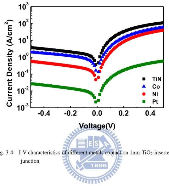
Fig.3-4 I-V characteristics of different metals contact on 1nm-TiO2-inserted
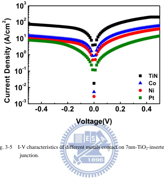
junction………...34 Fig.3-5 I-V characteristics of different metals contact on 7nm-TiO2-inserted
junction………..….35 Fig. 3-6 Schottky barrier heights versus Work functions of 1 and 7nm-TiO2-inserted
xi
Fig.3-7 Band diagrams of dielectric insertion junctions with (b) fixed oxide charges (c) dipoles at interface.……….………37 Fig.3-8 I-V characteristics of the TiN/Al2O3/Gejunctions before and after annealing at
300 °C, 400 °C and 600 °C for 30 minutes.………..….38 Fig.3-9 C-V characteristics of the Al/Al2O3(1nm)/SiO2(5nm)/Si and the
Al/SiO2(5nm)/Si capacitors.……….……..39
Fig. 3-10 I-V characteristics of the 1-nm-thick TiO2 inserted junctions before and after
annealing at 300 °C, 400 °C and 600 °C for 30 minutes.…………..…...…40 Fig. 3-11 I-V characteristics of the and 7-nm-thick TiO2 inserted junctions before and
after annealing at 300 °C, 400 °C and 600 °C for 30 minutes.……..……..41 Fig. 3-12 Schottky barrier height of 1nm and 7nm-TiO2-inserted junctions after
annealing at 300 °C, 400 °C and 600 °C for 30 minutes.……….……..…..42 Fig. 3-13 TEM micrographs of TiN/TiO2/Gejunctions after 600 °C for 30 minutes
annealing. No interlayer formed at the interface...……….………43 Fig. 3-14 XRD results of TiO2 layer after (a) 300 °C (b) 400 °C (c) 600 °C
annealing………. 44
Chapter 4
Fig. 4-1 I-V characteristics of NiGe MSB junctions activated at 400 °C, 450 °C and 500 °C for 30 minutes, current of NiGe without implantation junction is also shown.……….…51 Fig. 4-2 I-V characteristics of NiGe MSB junctions activated at 500 °C for 10, 30,
50, and 70 minutes………..………...52 Fig. 4-3 Sheet resistance values of NiGe filmes formed at 400 °C, 500 °C, 550 °C,
and 600 °C for 30 seconds…………...….………..53 Fig. 4-4 SEM images of NiGe filmes formed at (a) 400 °C, (b) 500 °C, (c) 550 °C,
xii
and (d) 600 °C for 10 seconds…………...………….………54 Fig. 4-5 Sheet resistance values of NiGe films with or without implantation after different post annealing temperature and time………..………….55 Fig. 4-6 Sheet resistance values of NiGe, NiSi, and NiGe with Si insertion films at different formation temperature for 30 seconds……….56 Fig. 4-7 SEM images of NiGe with Si-insertion filmes formed at (a) 400 °C, (b) 500
°C, (c) 550 °C, and (d) 600 °C for 10 seconds………….…..………57 Fig. 4-8 Sheet resistance values of NiGe and NiGe with Si films after MSB formation with activation temperature at 500 °C and 550 °C for different times………...58 Fig. 4-9 I-V characteristics of the MSB junctions after different activation
temperature 500 °C and 550 °C for 30 minutes………..…...………59 Fig. 4-10 I-V characteristics of NiGe with Si-insertion MSB junctions activated at 550 °C for different times………...………60 Fig. 4-11 SRP profiles for MSB junctions activated at 550 °C for 30 and 50 minutes, direct implantation to Ge sample activated at 550 °C for 10 seconds is also shown……….61 Fig. 4-12 I-V characteristics of the MSB junctions and the conventional direct
implantation to Ge junction………....62
Chapter 5
Fig. 5-1 I-V characteristics of the 550 °C annealed MSB junction and the 7-nm-thick TiO2 inserted junction before/after
1
Chapter 1
Introduction
1-1 Why Studying Germanium
In 1947, John Bardeen and Walter Brattain fabricated the first transistor using Ge as the semiconducting material at Bell Laboratories, by which they got 1956 Nobel Prize in Physics, along with William Shockley. From then on, Ge had been the predominant material for solid-state devices through 1950s and early 1960s. But during 1960s, once the crystal growth technology of Si became mature, Ge was quickly replaced by Si due to two major reasons: (1) Ge has smaller band gap (~0.67eV at room temperature) than Si resulting in larger leakage current and, most importantly, (2) Ge dioxide is water-soluble, which would produce many problems with device fabrication. Then with metal oxide semiconductor field effect transistors (MOSFETs) became the most important device, the excellent qualities of thermally grown Si dioxide as gate dielectric for Si resulted in more researches on Si instead of Ge.
In recent years, because of the device scaling limits, many methods have been proposed to improve devices performance. One of the most significant methods is that replacing Si dioxide gate dielectric with high-dielectric-constant (high-k) materials like HfO2 [1]. With the implement of the high-k dielectric, the lack of high-quality
native oxide with Ge becomes much less significant and because Ge has better electron (3900 vs 1400 cm2/Vs) and hole (1900 vs 500 cm2/Vs) bulk mobility than Si, it becomes one of the potential candidates to replace Si as next generation channel material.
2
However, Ge still encounters many challenges on MOSFET fabrication. First, Ge devices have high off-state leakage current because of the narrow band gap, which will introduce large tunneling current due to gate induce drain leakage (GIDL) effect as well as generation/recombination current. Second, the low solid-state solubility of dopants in Ge causes incomplete activation [2]. In addition, dopants diffusion with defects during annealing is more severe in Ge than in silicon, which would make it difficult to implement shallow and low resistivity source/drain junctions [3]. Although Ge p+/n junctions with high activation level of boron have been demonstrated [4,5], high performance n+/p junctions have not achieved because of the solid-state solubility and dopant diffusion limits. Third, the contact resistance at the metal/n+ Ge contact is large due to the high Schottky barrier height at the metal/n-Ge interface, which comes from Fermi level pinning effect [6,7] and results in high parasitic resistance so that degrading the on current of Ge NMOSFET. To improve the performance of Ge NMOSFET, contact resistance is one of the major problem has to be solved.
1-2 Contact Resistance and Fermi Level Pinning in Germanium
To reduce contact resistance of metal/Ge contacts, doping concentration and Schottky barrier height are the most critical factors have to be improved. Unfortunately, n-type doping concentration in Ge is very difficult to be increased because dopant diffusion is fast and the solid-state solubility is low in Ge. On the other hand, Schottky barrier height is also hard to be decreased due to Fermi level pinning. To deal with the Fermi level pinning problem, first we have to understand how Schottky barrier formed and its relationship with contact resistance.
3
1-2-1. Schottky Barrier Formation
When a metal is contacted with a semiconductor, a potential barrier will form at the interface due to the difference in the work functions between these two materials. The energy band diagrams in Fig.1[8] illustrate the process of the barrier formation. Fig.1-1(a) shows the electron energy band diagram of a metal of work function φm and an n-type semiconductor of work function χ + φn, where χ is the
semiconductor electron affinity and φ n is the difference between Fermi energy and
conduction band edge of semiconductor. According to the Einstein relation, the Fermi levels of the two materials must come into coincidence when electrostatic equilibrium is established, the electrons which have higher energy will transport to another material till the Fermi level of the two sides are equal, as shown in Fig.1-1(b). As the electrons move out of the semiconductor into the metal, the free electron concentration in the semiconductor region near the interface decreases, which causes the band bending of the semiconductor and forms a potential barrier at the interface, as shown in Figs.1-1(c) and 1-1(d). This potential barrier is called Schottky barrier, which plays an important role on the current transport of the metal-semiconductor contact.
In electrostatic equilibrium, the Fermi levels must be aligned at the interface, the Fermi level in the metal would move by an amount of equal to φm – (χ + φn) the
difference between the two thermionic work functions amounting to, where χ is the electron affinity and φ m is the metal work function. The final barrier height will
4
1-2-2. Contact Resistance
In general, contact resistance is described as
D bn c c c N m A R * 2 exp , where ρ c is the specific contact resistance, Ac is the contact area, ɛ is the dielectric constant, m* is the electron mobility of the semiconductor, ND is the doping
concentration, and φ bn is the Schottky barrier height. If we want to reduce contact
resistance, there are two strategies we can do: (1) increasing the doping concentration or (2) decreasing the Schottky barrier height. For several years in semiconductor industry, the effect of raising doping concentration at the CMOS source/drain region is significant, but doping concentration is too hard to be increased in Ge because of the solid-state solubility limit. So how to decrease the Schottky barrier height is an important issue for improving the metal/Ge contact resistance.
1-2-3. Fermi-Level Pinning
Fermi-level pinning effect means that when metal contacts with Ge, the Schottky barrier height almost does not change with the metal work function, just like Fermi level is pinned at a local energy level in semiconductor band gap. In other words, the relationship of φbn = φm – χ has to be modified to φbn = S (φm- φCNL) +
(φCNL- χ), where S is the pinning factor defined as dφbn/dφm and φCNL is the
semiconductor charge neutrality level. The pinning factor ranges from 0 to 1. If S approaches to 1, it means that the pinning effect is not apparent. On the contrary, if S approaches to 0, the pinning effect is significant and the semiconductor Fermi level would be pinned at φCNL, which makes Schottky barrier height to be nearly a constant
value with any metal.
5
states at a local position in band gap as shown in Fig.1-2 [9], when Fermi-level moves to there, a large number of carriers would flow into another material which has a lower Fermi energy to make the Fermi level be aligned with each other. As a consequence, semiconductor Fermi level is almost not changed till the junction being electrostatic equilibrium.
Surface states come from two factors, surface dangling bonds and metal-induced gap states (MIGS). The MIGS is caused by metal electron wave function penetrating into the semiconductor band gap [10]. In general, Fermi level would be pinned at the semiconductor charge neutrality level (CNL). The position of the CNL is determined by the weights of the conduction band (acceptor-like states) and valence band derived states (donor-like states). For Ge, it is shown experimentally [6] that the CNL lies about 0.1 eV above the valence band edge. The CNL and Fermi level will affect the interface charges. If the Fermi level lies below the CNL, donor-like states would be empty and is positively charged. On the other hand, if the Fermi level is above the CNL, acceptor states would be filled with electron and is negatively charged. Energy considerations thus make it favorable for the Fermi level to be aligned with the CNL. The result of the Fermi level pinning is the Shottky barrier height on n-type Ge is higher than 0.5 eV no matter what kind of metal is used. Such a high Schottky barrier height results in a high contact resistance at source and drain, and thus a poor driving capability of the NMOSFET.
1-3 Methods for Fermi Level Depinning
Because of Fermi-level pinning, the Schottky barrier height of metal/Ge contact is difficult to be reduced using metals with different work functions. But recent experiments have demonstrated that Fermi level can be depinned by the
6
following two methods. The first method is surface passivation, which reduces the number of dangling bonds at the Ge surface so that surface states would be decreased and then the Fermi level pinning effect is relaxed. Surface passivation could be achieved through several techniques, such as (NH4)2S solution immersion [11],
implantation of sulfur into Ge [12], and CF4 plasma treatment [13]. The second
method is inserting a thin dielectric layer between metal and Ge as a tunneling barrier. Several dielectrics have been employed. They are Si3N4 [14,15], Ge3N4 [16], MgO
[17,18], Al2O3 [19,20], and TiO2 [21,22]. The role of the thin dielectric layer is
theoretically considered as either to passivate the semiconductor surface states and/or reduce the metal-induced gap states by suppressing the penetration of wave function of the metal into the band gap of Ge. However, inserting an insulator may introduce a large tunneling resistance and limit the conduction current.
The tunneling resistance is dominated by tunneling width and the conduction band offset (CBO) between the inserted dielectric and Ge. It was pointed out that TiO2 may be a good material since it has a nearly zero CBO to Ge so that the
tunneling resistance is small [21]. The band diagrams of Al2O3/Geand TiO2/Geare
shown in Fig.1-3. By inserting TiO2 as the depinning layer on Ge, the effective
Schottky barrier height can be reduced to about 0.1 eV with Al/TiO2/Ge structure
[22].
The actual physical mechanism for the Fermi level depinning by inserting an dielectric layer has not been clear so far. Some researches indicated that there would be a dipole formed at the interface which causes additional potential drop to reduce the effective Schottky barrier height [15,23,24]. The other research considered that there would exist many fixed charges in the dielectric which also causes extra band bending so the Schottky barrier height is decreased [25].
7
1-4 Germanium Metal Contact
1-4-1. Metal Germanide
With CMOS devices scaling down, the parasitic resistance at the source/drain region contributes to larger and larger proportion of the total resistance. In order to solve this issue, self-aligned metal silicide (salicide) process had been proposed since 1980s. Around many kinds of metals, nickel silicide has the advantages of low sheet resistance, low forming temperature, no line-width dependence, and less silicon consumption during the silicide formation, so nickel silicide has been extensively used in current CMOS fabrication.
Although nickel germanide has higher resistivity than nickel silicide which would induce larger parasitic resistance at device source/drain region, nickel germanide is a better choice over the other metal germanides. It has been reported that high processing temperatures are required to form low resistivity titanium germanide (>800 °C) and cobalt germanide (>500 °C) [26], while nickel germanide can be formed at temperature as low as 270 °C [27,28]. Such a low processing temperature can be used with high-k gate stack without degradation, which makes nickel germanide more suitable for Ge device fabrication.
However, it has been found that nickel germanide is thermally unstable after annealing at temperatures above 500 °C with prominent grain growth and then broken into many small islands [26]. As a result, the film becomes discontinuous and the resistivity increases apparently. To improve the thermal stability of nickel germanide, alloying method has been proposed and widely studied, in which additive metals are introduced by alloyed target [29-31], or by inserting an ultrathin interlayer between nickel and germanium before germanidation [32-34]. With these metals incorporated in the nickel germanide films, the agglomeration effect can be
8 postponed.
1-4-2. Dopant Activation
In advanced CMOS processes, source/drain doping is formed by ion implantation because it can control doping concentration precisely and decouple the doping concentration and the doping profile. However, ion implantation produces many crystal defects in substrate due to energy transfer which would enhance dopant diffusion. Due to high diffusion coefficients and low solid-state solubility of n-type dopants in Ge, it is hard to achieve high percentage dopant activation [35,36]. Besides, n-type dopant diffusion is further enhanced by defects introduced by ion implantation [3], and high dosage implantation will aggravate this problem.
There were many methods trying to fabricate high doping concentration and shallow junction in Ge: (1) Laser annealing, with a nanosecond annealing and the small melting area, the dopant would not diffuse far from surface in such a short period and the doping concentration was very high because of the high temperature annealing [37,38]; (2) Co-sputter of P and Sb [39]; (3) Gas phase doping, with nearly no defect in substrate during annealing, the dopant diffusion effect could be suppressed and the device leakage current could be improved [40].
1-5 Motivation
This thesis will focus on how to improve the metal/Ge contact resistance through dielectric insertion and modified Schottky barrier (MSB) methods. The former method is trying to mitigate the Fermi level pinning effect and make Schottky barrier height decrease but it is not compatible with the self-aligned process, while the latter method is trying to enhance the dopant concentration at the metal/Ge
9
interface and it can be integrated with the self-aligned process.
As mentioned in the section 1-3, the Schottky barrier height can be reduced significantly by inserting an dielectric layer between metal and Ge. And it has been demonstrated that TiO2 has the best efficiency. However, the physical mechanism
and the process stability are not clear. In this these, TiO2 and Al2O3 were used to
reduce the Schottky barrier height on Ge. The thickness effect and the post deposition annealing effect on the contact are investigated. Besides, metals with different work functions are used to clarify how the TiO2 layer affects the Fermi
level pinning effect.
Recently, modified Schottky barrier (MSB) junctions have been proposed to improve the contact resistance. The MSB junction is a Schottky junction with a very thin and high doping concentration layer at the metal/semiconductor interface which can make the Schottky barrier thinner so that the tunneling resistance decreases. It can be accomplished by either dopant segregation (DS) [41-43] or implantation-to- silicide (ITS) [44- 47] process. The former process performs ion implantation before metal deposition on the semiconductor. During the silicidation process, the dopants are activated and segregated at the silicide-semiconductor interface by the snow-plow effect. On the contrary, in the ITS process, the dopants are implanted into silicide and then annealed at a low temperature to make them diffuse out from silicide to silicon and segregate at the interface. A thin and high doping profile at the edge of the silicide can be obtained. We try to use this process on Ge. Dopants are implanted into germanide instead of Ge so that the number of defects formed in substrate during ion implantation is reduced, which might mitigate dopant diffusion effect during dopant activation, and a thin and high concentration doping profile at germanide/Ge interface is expected. Finally, NiSi has lower sheet resistance and better thermal stability than NiGe. If a thin Si layer is inserted between Ni and Ge,
10
NiSi will be the main phase instead of the NiGe. The sheet resistance and thermal stability is expected to be improved. This thesis will examine this technique.
1-6 Thesis Organization
The organization of this thesis is described below. Chapter 1 introduces the characteristics of Ge and problems with n-type Ge metal contact. Methods to reduce contact resistance for Ge are also discussed. Chapter 2 describes the fabrication process of the samples, including the recipes of the etch process and device structures. Material and electrical analysis methods are also introduced.
Chapter 3 is studying on dielectric insertion junctions, first shows the current improvement by Al2O3 and TiO2 inserted dielectric layers and different TiO2
thicknesses, and how the dielectric insertion method affects the Schottky barrier height depinning, finally studying on the annealing effect of the dielectric insertion junctions. Chapter 4 is studying on modified Schottky barrier junctions, first shows current of the MSB junctions with different activation temperature and time, then describes the thermal stability problem of NiGe films and the improvement by incorporating Si into NiGe films, finally makes a comparison of doping profiles and junction currents between MSB and direct implantation to Ge samples.
Chapter 5 summarizes the experiment results and makes some conclusions on the Ge contact improvement by the two methods. Future works are also suggested.
11
Fig. 1-1 Formation of the Schottky barrier as metal approaches semiconductor surface[8].
12
Fig.1-2 Schematic illustration of Fermi level pinning of a semiconductor surface with non-uniformly distributed surface states[9].
13
14
Chapter 2
Experiments
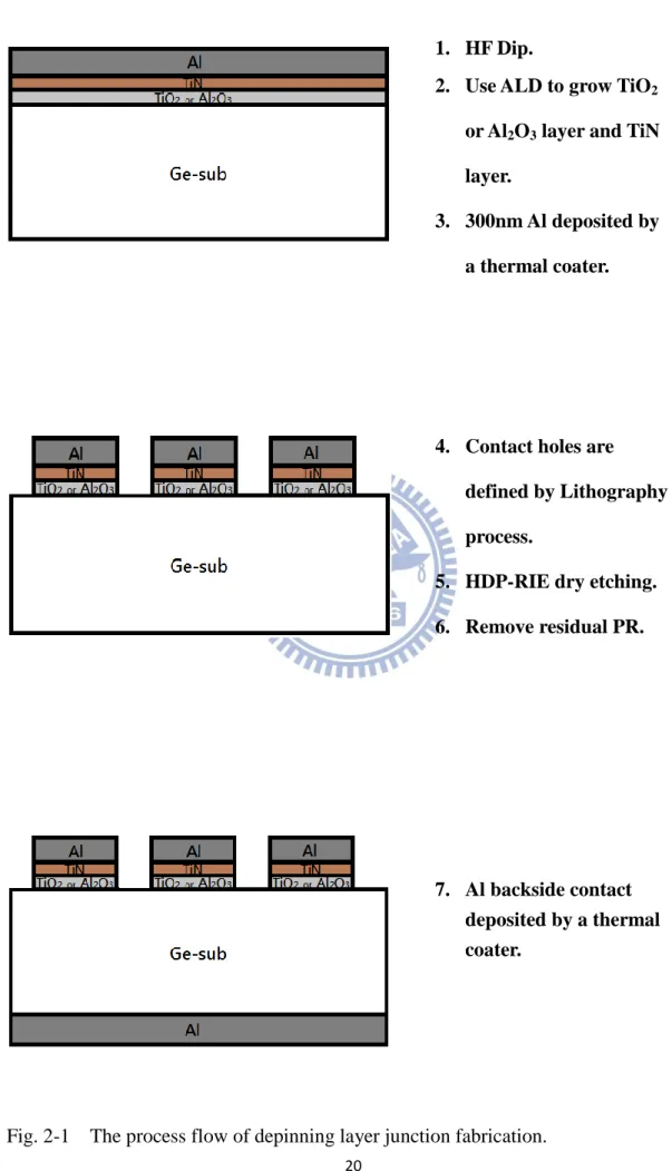
2-1 Device Fabrication
2-1-1. Dielectric Insertion Layer Junctions
N-type Sb doped Ge wafer with resistivity about 0.01 ohm-cm was used. Samples were dipped in diluted HF solution (H2O:HF = 20:1) and DI-water for one
minute circularly by three times to clean the surfaces. Then samples were loaded to an atomic layer deposition (ALD) chamber to deposit thin dielectric layers immediately. There are two kinds of insertion layer in this study, one is Al2O3 and another is TiO2.
The Al2O3 layer was deposited using Trimethylaluminium (TMA) and H2O as
precursors. The TiO2 layer was deposited using Tetrakis(dimethylamino) titanium
(TDMAT) and H2O as precursors. The deposition cycle was composed of one H2O
pulse and one TMA/TDMAT precursor pulse at temperature 250 °C. For the Al2O3
sample, the thickness is 1 nm grown by 11 cycles. For the TiO2 sample, the
thicknesses are 1 nm and 7 nm grown by 22 and 154 cycles, respectively. Some of these samples were then deposited by a 5-nm-thick TiN layer in the same ALD chamber using TDMAT as precursor and N2 plasma.
After ALD deposition, samples with TiN layer were annealed in vacuum furnace at 300 °C, 400 °C, and 600 °C for 30 minutes. Then a 300-nm-thick Al was deposited on these samples by a thermal coater and the contact metal was patterned by a typical lithography process and high density plasma - reactive ion etching (HDP-RIE) with Cl2 and BCl3 as the reaction gas. Finally, after removing the native oxide on the
sample backside by buffered oxide etchant (BOE), backside contact was completed with a 300-nm-thick Al deposition by a thermal coater. The schematic diagram of the
15 process flow is shown in Fig. 2-1.
The TiO2-inserted samples without TiN contact metal were deposited with
different metals including Pt, Ni, and Co and the contact metal was patterned by lift-off process. Pt and Ni were deposited by a sputter system. The deposition rate and thicknesses were 0.6 nm/min and 20 nm at Ar gas flow rate at 24 sccm, respectively, for Pt, and 3 nm/min and 100 nm at Ar gas flow rate at 100 sccm, respectively, for Ni. Co was deposited by an e-gun system with a deposition rate of 1.2 nm/min and a thickness of 80 nm. The other processes were identical to those of the samples using TiN as contact metal. The main process recipes of all samples are summarized in Table 2-1.
Al2O3 capacitors are made to extract the fixed charge density in the Al2O3 before
and afterannealing. N-type silicon wafer with resistivity of 15~25 Ω-cm was used. After RCA clean, a 5-nm-thick dry oxide was grown by a horizontal furnace, then samples were deposited a 1-nm-thick Al2O3 by an ALD system, the deposition
condition was identical to that of the Al2O3 insertion layer described in previous
sub-section. After deposition, samples were annealed in vacuum furnace at 300 °C, 400 °C, and 600 °C for 30 minutes. Then a 300-nm-thick Al was deposited by a thermal coater and patterned by typical lithography and lift-off process. Finally, after removing the native oxide on the sample backside by buffered oxide etchant (BOE), a 300-nm-thick Al was deposited by a thermal coater as backside contact.
2-1-2. Modified Schottky Barrier (MSB) Junctions
The Ge substrate and initial clean process are identical to those of the dielectric insertion samples. After cleaning, a 400-nm-thick Tetraethyl orthosilicate (TEOS) SiO2 were deposited by a plasma enhanced chemical vapor deposition (PECVD)
16
system at 350 °C. The contact area was patterned by typical lithography process and BOE etching. The residual photo-resist was removed by sonicating in acetone.
Both blanket and patterned samples were dipped in diluted HF solution (H2O:HF
= 100:1) to remove native oxide. A 20-nm-thick Si film was deposited on some samples by a sputter system, the process pressure is 7.6 mTorr and the Si deposition rate is 1.2 nm/min with Ar gas flow rate at 24 sccm. After Si deposition,samples were annealed in a vacuum furnace at 400 °C for 30 minutes to densify the Si film. Using typical lithography process, the Si outside contact hole was etched by poly-Si etchant (HNO3:H2O: NH4F = 64:33:3) and residual photo-resist was removed by sonicating in
acetone. Then after dipping in diluted HF solution (H2O:HF = 100:1), samples
with/without Si film were all sputtered a Ni/TiN film to a thickness of 10 nm/10 nm. The Ni deposition rate is 3 nm/min with Ar gas flow rate at 100 sccm. The TiN deposition rate is 4.2 nm/min with Ar gas flow rate at 100 sccm and N2 gas flow rate
at 4 sccm.
After the Ni/TiN deposition, samples were annealed in N2 ambient by a rapid
thermal annealing (RTA) system at 400 °C, 500 °C, 550 °C, 600 °C for 30 seconds to form nickel germaniude. The TiN and the unreacted Ni was selectively etched by hot HCl solution.
The 500 °C annealed samples were implanted by As+ at 10 keV to a dose of 5x1015 cm-2. Direct implantation into Ge samples with implantation energy 10 keV to a dose of 2x1015 cm-2 were alsofabricated.Before dopant activation, a 10-nm-thick TEOS oxide was deposited to avoid dopant out-diffusion. The MSB annealing was performed in a vacuum furnace with different thermal budgets. The annealing conditions are summarized in Table 2-2. After dopant activation, the capped oxide was etched by diluted HF solution (H2O:HF = 100:1) and the device fabrication was
17 schematic diagram of this process is in Fig. 2-2.
2-2 Material Analysis and Electrical Measurement
Several materal analysis techniques including X-ray Diffraction (XRD), Transmission Electron Microscopy (TEM), Scanning Electron Microscopy (SEM), and Spreading Resistance Profiling (SRP) were used in the study. Sheet resistance was measured by a four point probe system on blanket samples. Device forward/reverse bias current-voltage characteristics were measured by the semiconductor analyzer of model Agilent 4156C.
XRD analysis is used to observe the crystallization condition of the TiO2 layer
after annealing at different temperatures; it can tell us how annealing process affects the crystalline structure of the TiO2 layer. TEM analysis is used to inspect the
microstructure of the TiO2/Ge structure to reveal if there has an interfacial layer
formation after annealing.
SEM can help us to inspect the surface morphology of the nickel germanide. In general, nickel germanide surface would be rough due to agglomeration effect after high temperature annealing. With SEM image, we can see how agglomeration effect affects the nickel germanide resistance. SRP is used to analyze the dopant distribution of the MSB junction after thermal activation.
Schottky barrier height was extracted by the thermionic emission model, which
is given by * 2 kT 1 qV kT q e e T A J Bn
, where Ac is the Richardson constant and T is
the absolute temperature. If V is negative and -V>>3kT/q, then the function can be simplified to ln(J/A*T2) = -qφBn /kT. Plot ln(J/A*T) as a function of q/kT, the slope is
18
function has to be multiplied by an additional tunneling term, which is proportional to tunneling width and tunneling barrier height [19]. But in general, these two factors do not change with temperature, so we can still extract the Schottky barrier height by the same procedure as if there is no insertion layer.
19
Thickness Annealing recipe Contact metal Al2O3 1nm 300 °C for 30min 400 °C for 30min 600 °C for30min TiN TiO2 1nm 7nm 300 °C for 30min 400 °C for 30min 600 °C for30min TiN Co Ni Pt
Table 2-1 The main process recipes of depinning layer junction samples.
Activation temperature Activation time (minutes) NiGe 400 °C, 450 °C, 500 °C
for 30 minutes
10, 30, 50, 70 at 500 °C
NiGe with Si 550 °C for 30 minutes 10, 30, 50, 70 at 550 °C Table 2-2 The annealing conditions of MSB junction samples.
20
Fig. 2-1 The process flow of depinning layer junction fabrication.
1. HF Dip.
2. Use ALD to grow TiO2
or Al2O3 layer and TiN
layer.
3. 300nm Al deposited by a thermal coater.
4. Contact holes are defined by Lithography process.
5. HDP-RIE dry etching. 6. Remove residual PR.
7. Al backside contact deposited by a thermal coater.
21
6. HF Dip.
7. Use PECVD to grow TEOS oxide 400nm. 8. Active region define by
Lithography process. 9. Oxide etched by BOE
and remove residual PR. 10. Ni 10nm and TiN 10nm are deposited by a sputter system. 11. Germanidation by a RTA system.
12. Residual metals are etched by hot HCl solution.
22
Fig. 2-2 The process flow of MSB junction fabrication.
1. Implanted by As+ 10keV with dose 5x15 cm-2 2. TEOS oxide 10nm deposited by a PECVD system. 3. Doping activation by a vacuum furnace.
4. Oxide etched by diluted HF solution.
5. Al backside contact deposited by a thermal coater.
23
Chapter 3
Dielectric Insertion Junctions
3-1 Introduction of Dielectric Insertion Method
N-type Ge suffers from large contact resistance due to Fermi level pinning at the charge neutrality level which is about 0.09 eV above the Ge valence band. It has been reported that inserting a thin dielectric layer between metal and semiconductor could alleviate the Fermi level pinning effect [14]. Although this dielectric layer could reduce the Schottky barrier height, it also introduces large tunneling resistance due to the conduction band offset between the dielectric layer and Ge. If we want to obtain low contact resistance, the thickness of the dielectric layer has to be very thin to attain low tunneling resistance. Besides, the actual physical mechanism of this method has not been clear so far. There are three major explanations: (1) These dielectric layers can block the electron wave function from metal to semiconductor and therefore decrease the number of surface defects [14]. (2) There would be a dipole formed at metal/semiconductor interface which cause extra voltage drop to reduce the Schottky barrier height [15,23,24]. (3) There would be some fixed charges in the dielectric layer which could also cause extra voltage drop in the dielectric layer [25]. In this chapter, sequential experiments are designed to clarify which mechanism dominates the Schottky barrier height modulation.
3-2 Currents of the two Dielectric Insertion Junctions – Al
2O
3&
TiO
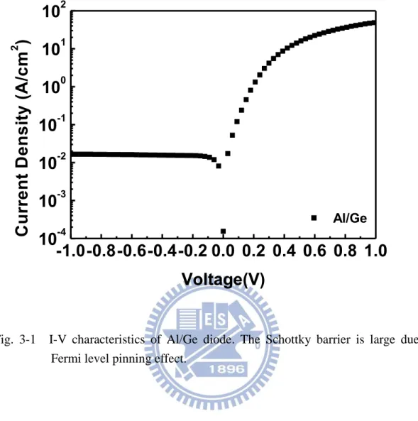
2Fig.3-1 shows the current-voltage (I-V) characteristics of the Al/Ge diode. According to the function φbn = φm – χ , the of Ge is about 4.05 eV and the φ m of
24
Al is about 4.1 eV so the ideal Shottky barrier height is about 0.05 eV, but the Shottky barrier height is about 0.53 eV extracted from the I-V curve, which confirms severe Fermi level pinning effect on Ge.
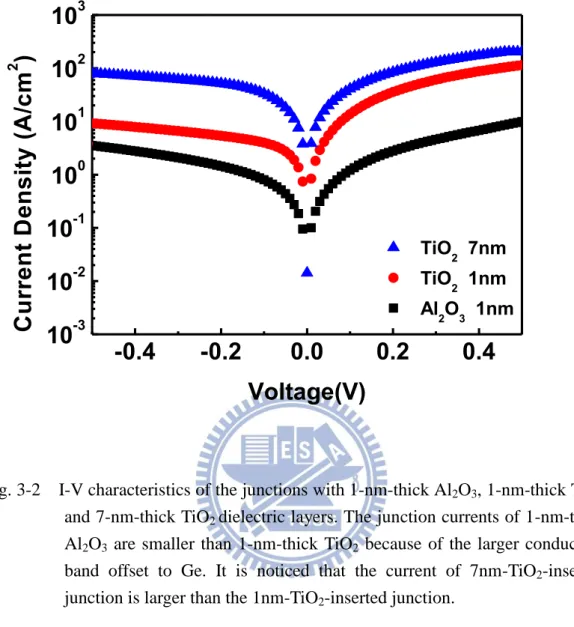
Fig.3-2 and Fig.3-3 show the I-V characteristics and the Schottky barrier heights, respectively, of the junctions with 1-nm-thick Al2O3, 1-nm-thick TiO2, and
7nm-thick TiO2 dielectric layers. The contact metal is a 5-nm-thick TiN layer
deposited by ALD process. The forward/reverse current ratio of these three samples decreases apparently in comparison with that of the simple Al/Ge diode. These results indicate that the Schottky barriers heights are very low. It can be also found that although the 1-nm-thick Al2O3 sample has near Schottky barrier height with
1-nm-thick TiO2 sample, its current density is still much smaller than 1-nm-thick TiO2
sample because the large conduction band offset of Al2O3 to Ge limits the current
conduction [22]. On the contrary, TiO2 has nearly zero conduction band offset to Ge
so it can not only decrease the Schottky barrier height but also make the tunneling resistance small.
In general, thicker dielectric layer will introduce higher tunneling resistance under the same tunneling barrier height. However, it is observed that the Schottky barrier height of the 7-nm-thick TiO2 sample is smaller than that of the 1-nm-thick
TiO2 sample. This phenomenon has been reported previously, but was not discussed
[22]. To clarify this effect, we first consider that thicker dielectric layer would suppress the MIGS effect more effectively because the metal electron wave function is exponentially decayed in the dielectric layer. Thus, the number of surface states caused by the MIGS will decrease with the increase of the dielectric layer thickness. If the MIGS effect is mitigated, the Fermi level pinning effect is mitigated, too. To verify this postulation, different metals are used as contact metal with 1-nm-thick and 7-nm-thick TiO2 layers to observe the Fermi level pinning effect of these junctions.
25
3-3 Fermi Level Pinning Effect of TiO
2Dielectric Insertion
Junctions
Fig.3-4 and Fig.3-5 show the I-V characteristics of junctions with different contact metals. Four kinds of metals are used in this experiment; they are Pt, Ni, Co, and TiN which have work functions about 5.65 eV, 5.1 eV, 5 eV, and 4.5 eV, respectively. Metal with further lower work function is not used in this experiment because the Schottky barrier height of the 7-nm-thick TiO2 sample would be very
small (about 0.04 eV for TiN which work function is 4.5 eV) so that we can’t extract Schottky barrier height accurately due to most supply voltage is consumed on the parasitic resistance instead of the Schottky barrier. With higher work function metal, the current densities are lower, which indicates that Schottky barrier height increases with the work function.
Fig.3-6 shows the extracted Schottky barrier height of the 1-nm-thick and 7-nm-thick TiO2 samples with different contact metals. The Schottky barrier height of
the pure metal/Ge junctions is also shown in the figure 6. The slopes of the linear regression lines give the pinning factors S. The pinning factor is about 0.05 for the pure Ge junction which indicates the severe Fermi level pinning effect on Ge. For the junctions with TiO2 insertion layer, the pinning factors are about 0.14 and 0.12 for the
junctions with 1-nm-thick and 7-nm-thick TiO2, respectively. These values are larger
than that of the pure Ge junction which means that the Fermi level pinning effect is mitigated with the TiO2 insertion layer. However, the pinning factors are still much
smaller than 1. In the case of complete depinning, the pinning factor should approach to 1; the small values of the pinning factors indicate that the Fermi level pinning effect is not mitigated completely by the TiO2 insertion layer.
26
The improvement of pinning factor compared to pure Ge may come from alleviating of MIGS effect. However, it is worthy to notice that the pinning factors of both TiO2 thicknesses are about the same, which indicates that the depinning effect of
the 7-nm-thick TiO2 is not better than that of the 1-nm-thick TiO2. It is thus inferred
that the lower Schottky barrier height of the 7-nm-thick TiO2 sample than the
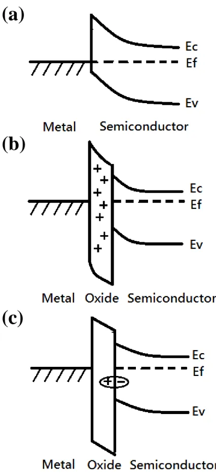
1-nm-thick sample is not due to the thicker dielectric layer suppresses the MIGS effect more effectively, but because that the pinning position is changed more for thicker TiO2 layer. The changed pinning position may result from two factors, fixed
oxide charges or dipoles formed at TiO2/Ge interface, both can introduce an additional
potential drop in the current conduction path and results in the reduction of the Schottky barrier height. The band diagrams of both cases are shown in Fig. 3-7.
To understand how fixed oxide charges affect the Schottky barrier height, we can examine the annealing effect on the junctions with insertion layer because the fixed oxide charges will be reduced after annealing.
3-4 Annealing Effect of Dielectric Insertion Junctions
Fig.3-8 shows the I-V characteristics of the TiN/Al2O3/Gejunctions before
and after annealing in vacuum at 300 °C, 400 °C and 600 °C for 30 minutes. It is observed that with the increased annealing temperature, the currents of the junctions decreased at all annealing temperatures. Chui and coworkers have also found this phenomenon, and they proposed that the Al2O3 layer has some fixed charges that
cause potential drop and change the electric field in the oxide. They observed that the capacitance-voltage curves of the MIS capacitors with different Al2O3 dielectric
thicknesses would be overlapped after annealing, so they considered the oxide charges in the Al2O3 were eliminated which caused the junction current decreased [25]. Only
27
one annealing condition was performed in their work. In this thesis, the junction current further decreases after 600 °C annealing. If the current reduction is due to the annealing of fixed charges, it must be supposed that the fixed charges are not completely eliminated at 300 °C for 30 minutes.
To verify the influence of fixed charges on the Schottky barrier height modulation, Al2O3 capacitor was fabricated to calculate the number of fixed charges
in the 1-nm-thick Al2O3 film. Because the 1-nm-thick Al2O3 is too thin so that the
tunneling current would be too high and the capacitance-voltage characteristic cannot be measured, a 5-nm-thick SiO2 was thermally grown to block the leakage current.
Fig.3-9 shows the C-V characteristics of the Al/Al2O3(1nm)/SiO2(5nm)/Si and the
Al/SiO2(5nm)/Si capacitors. The difference of the mid-gap voltage between the two
samples is about 0.05 V. According to the function Qox = Cox x V, where Qox is oxide charge density, Cox is accumulation capacitance, and V is mid-gap voltage difference, the Qox is about 2.27 x 1011 cm-2 in the 1-nm-thick Al2O3 layer. The
capacitance of a 1-nm-thick Al2O3 capacitoris about 7.8 x 10⁻⁶ F/cm2, to produce a 0.1
V voltage drop, the oxide charges have to be 4.87 x 1012 cm-2. We can infer that the number of fixed charges in such a thin dielectric layer is not sufficient for producing a large voltage drop to make the Schottky barrier height shifts more than 0.3 eV. Thus, it is recommended that the Schottky barrier height modulation of the Al2O3 inserted
junction ismainly caused by interface dipoles.
Fig.3-10 and Fig.3-11 show the I-V characteristics of the 1-nm-thick and 7-nm-thick TiO2 inserted junctions, respectively, before and after annealing in vacuum
at 300 °C, 400 °C, and 600 °C for 30 minutes. The corresponded Schottky barrier heights are shown in Fig.3-12. Similar to the Al2O3-inserted junctions, the conduction
current decreases after annealing. It is noticed that the Schottky barrier heights of the annealed 7-nm-thick TiO2 junction is still lower than that of the annealed 1-nm-thick
28
TiO2 junction. If the Schottky barrier height modulation mechanism of the TiO2
inserted junction mainly results from the fixed charges in TiO2 and these charges are
annealed-out completely, the Schottky barrier height of the 7-nm-thick TiO2 junction
should equal to that of the 1-nm-thick TiO2 junction. However, this prediction
conflicts with the experimental results. Therefore, it is recommended that the Schottky barrier height modulation of the TiO2-inserted junction ismainly caused by
interface dipoles, too. According to Fig.3-12, the trend of the increase of Schottky barrier height with annealing temperature of the two junctions are similar, probably there is a same mechanism for the increase of Schottky barrier height after annealing of these two junctions.
To observe if there is a new interfacial layer formed after annealing, the cross-sectional structure of the 600 °C annealed TiN/TiO2/Ge junction was inspected
by the high-resolution TEM and the micrograph is shown in Fig.3-13. It is clearly that there is no interfacial layer formed at the TiO2/Ge interface and the TiN/TiO2 interface.
The thin layer between Al and TiN is probable AlOx layer according to EDS analysis which was formed during Al deposition by a thermal coater. It would not affect the Schottky barrier height. The thicknesses of the deposited TiO2 and TiN layers are 7
nm and 5 nm, respectively. Their thicknesses after annealing are almost the same with the as deposited thicknesses which means that no chemical reaction between the three layers. This result suggests that the Schottky barrier height increment is not due to new layer formation after 600 °C annealing.
Fig.3-14 (a)-(c) show the XRD spectra of the 7-nm-thick TiO2-inserted
junction after annealing at 300 °C, 400 °C, and 600 °C for 30 minutes, respectively. The TiO2 and TiN layers remain in amorphous state after 400oC annealing. The (110)
crystalline phase of TiO2 isdetected on the 600 °C annealed sample, which means that
29
dielectric layer is crystallized, the dielectric constant will be higher than that in amorphous state, so the capacitance of COX = ɛ/ TOX would be higher and the voltage
drop of V = QOC / COX would be smaller. The QOC here includes fixed charges and
interface dipole charges. It is thus postulated that the crystallization of the inserting layer is one possible explanation of Schottky barrier height shift after annealing. Thicker dielectric results in smaller capacitance Cox, and the voltage drop of V = QOC / COX would be larger so that the Schottky barrier heights are modulated more.
The more effective Schottky barrier height modulation by 7-nm-thick TiO2 than that
by 1-nm-thick TiO2 might be explained by this postulation.
3-5 Summary of Dielectric Insertion Junctions
The effect and mechanism of Schottky barrier height modulation of the metal/n-type Ge Schottky junction by inserting dielectric layer are examined. Both Al2O3 and TiO2 insertion layer result very low Schottky barrier height than the sample
without insertion layer. The conduction current of the Al2O3–inserted junction is
smaller than that of the TiO2–inserted junction because of the larger conduction band
offset of Al2O3 to Ge.
Different metals are used to determine the Fermi-level pinning factor. The pinning factor of the TiO2-inserted junction is larger than that of the simple metal/Ge
junction but is still much smaller than 1. This result indicates that the Fermi level pinning effect is only slightly mitigated by the insertion layer. The pinning factor does not increases with the increase of the insertion layer thickness, which indicates that the modulation of Schottky barrier height is not due to the suppression of the MIGS effect by the inserted dielectric layer. The amount of the fixed charges in the inserted dielectric is extracted by a MIS capacitor. The value is too low to produce the
30
apparent Schottky barrier height modulation. It is recommended that the mechanism of the Schottky barrier modulation by inserting dielectric layer mainly comes from the interface dipoles.
The Schottky barrier height of the dielectric inserted junction is not thermally stable. The Schottky barrier height increases with the increase of annealing temperature. Since no interfacial layer formation can be observed at the TiN/TiO2 and
the TiO2/Ge interfaces, it may due to the crystallization of the dielectric layer so that
31
Fig. 3-1 I-V characteristics of Al/Ge diode. The Schottky barrier is large due to Fermi level pinning effect.
-1.0-0.8-0.6-0.4-0.2 0.0 0.2 0.4 0.6 0.8 1.0
10
-410
-310
-210
-110
010
110
2 Al/GeC
u
rr
e
n
t
D
e
n
s
it
y
(
A
/c
m
2)
Voltage(V)
32
Fig. 3-2 I-V characteristics of the junctions with 1-nm-thick Al2O3, 1-nm-thick TiO2,
and 7-nm-thick TiO2 dielectric layers. The junction currents of 1-nm-thick
Al2O3 are smaller than 1-nm-thick TiO2 because of the larger conduction
band offset to Ge. It is noticed that the current of 7nm-TiO2-inserted
junction is larger than the 1nm-TiO2-inserted junction.
-0.4
-0.2
0.0
0.2
0.4
10
-310
-210
-110
010
110
210
3C
u
rr
e
n
t
D
e
n
s
it
y
(
A
/c
m
2)
Voltage(V)
TiO2 7nm TiO2 1nm Al2O3 1nm33
Fig. 3-3 Schottky barrier height of the junctions with 1-nm-thick Al2O3, 1-nm-thick
TiO2, and 7-nm-thick TiO2 dielectric layers. 7nm TiO2-inserted junction
has lowest Schottky barrier height.
0.02
0.04
0.06
0.08
0.10
0.12
0.14
0.16
0.18
0.20
TiO2 7nm TiO2 1nmS
c
h
o
tt
k
y
b
a
rr
ie
r
h
e
ig
h
t(
e
V
)
Al2O3 1nm34
Fig. 3-4 I-V characteristics of different metals contact on 1nm-TiO2-inserted
junction.
-0.4
-0.2
0.0
0.2
0.4
10
-310
-210
-110
010
110
210
3 TiN Co Ni PtC
u
rr
e
n
t
D
e
n
s
it
y
(
A
/c
m
2)
Voltage(V)
35
Fig. 3-5 I-V characteristics of different metals contact on 7nm-TiO2-inserted
junction.
-0.4
-0.2
0.0
0.2
0.4
10
-310
-210
-110
010
110
210
3 TiN Co Ni PtC
u
rr
e
n
t
D
e
n
s
it
y
(
A
/c
m
2)
Voltage(V)
36
Fig.3-6 Schottky barrier heights versus Work functions of 1 and 7nm TiO2-inserted
junctions, pure metal/Ge junctions is also shown. The slopes of the linear regression lines give the pinning factors S. The pinning factors of the two samples are larger than the pure Ge junction but are still much smaller than 1 which indicatess the Fermi level pinning effect is just slightly mitigated. The pinning factor of 7nm TiO2-inserted junction is not larger than the
1nm TiO2-inserted junction indicates the lower Schottky barrier height is
due to the pinning position shifted more for 7nm TiO2-inserted junction.
2.8 3.2 3.6 4.0 4.4 4.8 5.2 5.6
0.0
0.1
0.2
0.3
0.4
0.5
0.6
0.7
S=0.0517
[6]S=0.1439
S=0.1255
TiO2_1nm TiO2_7nm Geb
a
rr
ie
r
h
e
ig
h
t(
eV
)
Work function(eV)
37
Fig. 3-7 Band diagrams of dielectric insertion junctions with (b) fixed oxide charges (c) dipoles at interface.
(b)
(a)
38
Fig. 3-8 I-V characteristics of the TiN/Al2O3/Gejunctions before and after annealing
at 300 °C, 400 °C and 600 °C for 30 minutes. Currents are all decreased with increased annealing temperature.
-0.4
-0.2
0.0
0.2
0.4
10
-410
-310
-210
-110
010
110
2 initial 300OC 30min 400OC 30min 600OC 30minC
u
rr
e
n
t
D
e
n
s
it
y
(
A
/c
m
2)
Voltage(V)
39
Fig. 3-9 C-V characteristics of the Al/Al2O3(1nm)/SiO2(5nm)/Si and the
Al/SiO2(5nm)/Si capacitors. The amount of fixed oxide charges in the 1nm
Al2O3 is a little.
![Fig. 1-1 Formation of the Schottky barrier as metal approaches semiconductor surface[8]](https://thumb-ap.123doks.com/thumbv2/9libinfo/8750401.205790/25.892.140.746.147.396/fig-formation-schottky-barrier-metal-approaches-semiconductor-surface.webp)
![Fig. 1-3 Band diagrams of Al 2 O 3 /Ge and TiO 2 /Ge structure [20].](https://thumb-ap.123doks.com/thumbv2/9libinfo/8750401.205790/27.892.135.762.107.444/fig-band-diagrams-al-ge-tio-ge-structure.webp)