行政院國家科學委員會專題研究計畫 成果報告
高介電常數閘極介電層材料製備與可靠性分析
計畫類別: 個別型計畫 計畫編號: NSC92-AT-7-009-001- 執行期間: 92 年 10 月 01 日至 93 年 12 月 31 日 執行單位: 國立交通大學電子工程研究所 計畫主持人: 林鴻志 共同主持人: 簡昭欣 計畫參與人員: 盧文泰 報告類型: 完整報告 處理方式: 本計畫可公開查詢中 華 民 國 94 年 4 月 6 日
高介電常數閘極介電層材料製備與可靠性分析
Preparation and characterization of high-K gate dielectric materials
Abstract
HFO2 is a promising alternative for replacing SiO2 in ULSI manufacturing. In this work,
we employ different gas plasma, i.g. N2O, NH3, and N2, to nitrify the HfO2 films in order to
obtain less bulk traps responsible to threshold voltage instability. In this work, we found that
HfO2 film with N2O plasma nitridation exhibits excellent properties, such as lower swing,
higher conductance and driving current. This is due to the N2O plasma nitridation can reduce
interface states and bulk traps in the HfO2 film, confirmed by using charge pumping
technique1) with different measurement method, i.e. fixed base, fixed peak and fixed
amplitude method.
Introduction
Charge trapping is an important concern in the CMOS devices with HfO2 gate dielectrics,
due to the large amount of bulk traps presented in the HfO2 films. Their presence can result in
the reliability degradation,2) mobility degradation3-7) and threshold voltage instability8-12). In
order to improve the film quality, a variety of nitridation techniques were used to incorporate
nitrogen into the high-k films.4,9-11) In this work, we utilized the N2O plasma treatment
following the HfO2 deposition, which possesses the advantage of low thermal budget for
preventing the HfO2 films from crystallization during processing. It was found that the
post-deposition N2O plasma treatment can not only effectively improve the electrical
characteristics of the pMOSFETs with the HfO2 gate stack, such as lower bulk traps, interface
states, mobility and the resultant higher driving current, but also reduce the gate leakage
current substantially.
Experimental
The pMOSFETs were fabricated on n-type (100) 150 mm wafers. After conventional
LOCOS isolation, standard RCA cleaning with a final HF-dip was performed, followed by the
growth of an intentional 0.6nm thin interfacial oxyntride layer (SiON) using rapid thermal
processing in a NO2 ambient at 700°C. Subsequently, an approximately 3nm HfO2 layer was
substrate temperature of 500°C. The physical thicknesses of the SiON layer and HfO2 film
were measured by the optical n&k analyzer. After deposition of the HfO2 films, some samples
were subjected to an additional N2O-gas, NH3-gas or N2-gas plasma treatment at the substrate
temperature of 300°C. Then, all samples were annealed in a N2 ambient at 600°C for 30s in
order to improve the film quality. A 250nm polycrystalline silicon (poly-Si) layer was directly
deposited by low pressure chemical vapor deposition (LPCVD) on top of the HfO2 films, and
then the gate electrode patterning was implemented through lithography and etching
processing. Subsequently, the extension and deep source/drains were formed by implantation,
which dopants were activated at 950°C with rapid thermal annealing (RTA) for 20s in a N2
atmosphere. After passivation, contact holes formation, Al metallization and patterning, the
forming gas annealing at 400°C was finally performed for 30minutes.
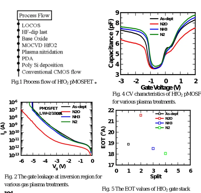
Fig. 2 and 3 shows the gate leakage current of PMOSFET with HfO2 gate stack
subjected to various post-deposited plasma treatment under inversion and accumulation
region, respectively. The gate leakage current could be reduced by N2O plasma treatment both
at inversion and accumulation region, especially at inversion region, reduction can be
achieved two order magnitude.
Fig. 4 shows the typical C-V characteristics of HfO2 gate stack with various plasmas
lower than that at strong accumulation region, which is due to the poly depletion effect. In
addition, the hump occurs at the depletion region for all samples. This may be due to the
interface states and it seems the N2O-treated sample exhibits no significant hump. Fig. 5
shows the EOT extracted from strong inversion for HfO2 gate stack with various plasma
treatment. The EOT for N2O-treated sample increases, but for NH3-treated and N2-treated
samples decrease. The slightly EOT for N2O-treated sample may be one of the reason for
reduced leakage current.
The values of subthreshold swing of pMOSFETs with HfO2 gate stack objected various
plasma treatment. It can be found that N2O plasma-treated sample shows smaller swing
resulted from lower interface states. However, the degradation of swing are observed for
NH3-treated and N2-treated samples. This may be due to the ion bombardment from the
plasma.
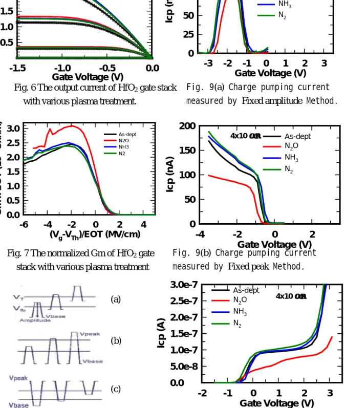
The influences of various plasma treatments on the driving current of the pMOSFETs
with HfO2 gate stack. The driving current can be enhanced by post-deposited N2O plasma
treatment for HfO2 gate stack with higher EOT. Those results may be ascribed to lower
interface states and higher normalized transconductance, as shown in Fig.7. However, the
higher driving current for NH3-treated and N2-treated samples is attributed to smaller EOT
In order to gain into investigations of the improvements for N2O-treated samples, the
charge pumping measurements are used to analyze the interface states and bulk traps in the
dielectrics. Recently, the CP measurement had been frequently employed to qualify the level
of bulk traps 12,13) in the HfO2 dielectrics using the fixed base sweep and/or the fixed peak
sweep, as indicated in Fig. 8(b) and Fig. 8(c), respectively. The measured results of charge
pumping measurements are shown in the Figure 9. We can find that the interface states and
bulk traps 12,13) in the HfO2 dielectrics can be reduced by the post-deposition N2O plasma
treatment, resulted in the higher driving current and lower interface states even that it has
higher EOT.
Reference
1) E. A. Kerber et al., 2003 IRPS, pp.41.
2) S. Zafar, A. Callegari, E. gusev, and M. Fischetti: J. Appl. Phys. 93 (2003) 9298.
3) E. Gusev, D. A. Buchanan, E. Cartier: Int. Electron Device Meet. Tech. Dig., 2001, p. 451.
4) H. -J. Cho, C. Y. Kang, C. S. Kang, R. Choi, Y. H. Kim, M. S. Akbar, C. H. Choi, S. J.
Rhee, and J. C. Lee: IEEE Semiconductor Device Research Symposium, 2003, p. 68.
5) Y. Morisaki, T. Aoyama, Y. Sugita, K. Irino, T. Sugii, and T. Nakamura: Int. Electron
Devices Meet. Tech. Dig., 2002, p. 861.
Nishiyama: Int. Electron Device Meet. Tech. Dig., 2001, p. 459.
7) M. Koyama, A. Kaneko, T. Ino, M. Koike, Y. Kamata, R. Iijima, Y. Kamimuta, Takashima,
M. Suzuki, C. Hongo, S. Inumiya, M. Takayanagi and A. Nishiyama: Int. Electron
Devices Meet. Tech. Dig., 2002, p. 849.
8) R. Choi, C. S. Kang, B. H. Lee, K. Onishi, R. Nieh, S. Gopalan, E. Dharmarajan, and J. C.
Lee: Symp. VLSI Tech. Dig., 2001, p. 15.
9) M. Koyama, A. Kaneko, T. Ino, M. Koike, Y. Kamata, R. Iijima, Y. Kamimuta, Takashima,
M. Suzuki, C. Hongo, S. Inumiya, M. Takayanagi and A. Nishiyama: Int. Electron
Devices Meet. Tech. Dig., 2002, p. 849.
10) K. Onishi, S. K. Chang, R. Choi, Hag-Ju Cho; Gopalan, S, R. E. Nieh, S. A. Krishnan, and
J. C. Lee: IEEE Trans. Electron Devices 50 (2003) 384.
11) H. -J. Cho, C. S. Kang, K. Onishi, S. Gopalan, R. Nieh, R. Choi, E. Dharmarajan, J. C.
Lee: Int. Electron Device Meet. Tech. Dig., 2001, p. 655.
12) A. Kerber, E. Carter, L. Pantisano, M. Rosmeulen, R. Degraeve, T. Kauerauf, G.
Groeseneken, H. E. Maes, and U. Schwalke: Proc. 41th Int. Reliability Physics Symp,
Texas, 2003, p. 41.
13) A. Kerber, E. Carter, L. Pantisano, M. Rosmeulen, R. Degraeve, G. Groeseneken, H. E.
Fig.1 Process flow of HfO2 pMOSFET。
Fig. 2 The gate leakage at inversion region for various gas plasma treatments.
Vg (V) -6 -5 -4 -3 -2 -1 0 Ig (A) 10-13 10-12 10-11 10-10 10-9 10-8 10-7 10-6 As-dept N2O NH3 N2 PMOSFET L/W=2/10µm
V
g(V)
0
1
2
3
4
5
6
I
g(A
)
10
-1210
-1110
-1010
-910
-810
-710
-610
-510
-4 As-dept N2O NH3 N2 PMOSFET L/W=2/10µmFig. 3 The gate leakage at accumulation region for various gas plasma treatments.
Gate Voltage (V)
-3
-2
-1
0
1
2
Ca
p
a
ci
ta
n
c
e
(p
F)
3
4
5
6
7
8
9
As-dept N2O NH3 N2Fig. 4 CV characteristics of HfO2 pMOSFET for various plasma treatments.
Split 0 1 2 3 4 5 6 EOT ( o A) 17 18 19 20 21 22 As-dept N2O NH3 N2
Fig. 5 The EOT values of HfO2 gate stack with various plasma treatment.
Method As- dept N2O NH3 N2 Swing value ~81 ~76 ~87 ~87
Table. 1 The swing values of HfO2 gate stack with various plasma treatment.
Fig. 8 The methods of various charge pumping measurements.(a) Fixed amplitude (b) Fixed Base (c) Fixed peak。
(a)
(b)
(c)
Fig. 9(c) Charge pumping current measured by Fixed base Method.
Gate Voltage (V) -2 -1 0 1 2 3 Icp ( A ) 0.0 5.0e-8 1.0e-7 1.5e-7 2.0e-7 2.5e-7 3.0e-7 As-dept N2O NH3 N2 4x10 µm Gate Voltage (V) -1.5 -1.0 -0.5 0.0 I d (1 0 -4 A) 0.5 1.0 1.5 2.0 2.5 3.0 As-dept N2O NH3 N2
Fig. 6 The output current of HfO2 gate stack with various plasma treatment.
(Vg-VTh)/EOT (MV/cm) -6 -4 -2 0 2 4 Gm x EOT (10 -4 Sxnm) 0.0 0.5 1.0 1.5 2.0 2.5 3.0 As-dept N2O NH3 N2
Fig. 7 The normalized Gm of HfO2 gate stack with various plasma treatment
Gate Voltage (V) -3 -2 -1 0 1 2 3 Icp ( n A ) 0 25 50 75 100 125 As-dept N2O NH3 N2 4x10 µm
Fig. 9(a) Charge pumping current measured by Fixed amplitude Method.
Gate Voltage (V) -4 -2 0 2 Icp ( n A) 0 50 100 150 200 As-dept N2O NH3 N2 4x10 µm
Fig. 9(b) Charge pumping current measured by Fixed peak Method.