新穎非對稱準光子晶體共振腔之製程技術與其WGM模態特性探討
67
0
0
全文
(2) 新穎非對稱準光子晶體共振腔之製程技術與其 WGM 模態特性探討. 研究生:曾仲銓 指導老師:李柏璁. 教授. 國立交通大學光電工程研究所碩士班. 摘要. 在本篇論文當中,我們使用三維有限時域差的方法去計算出兩種非對稱性光子晶體 雷射的共振頻譜、和共振場圖。這些有效的計算方法幫助我們能最佳化我們的光子晶體 設計,並且把這些設計確實的應用在我們的製程當中。. 在製程的篇章中,主要分為兩大部分去介紹,分別是準光子晶體雷射底部是高反射 率布拉布拉格反射鏡及底部為中央支柱兩種結構的製程。首先主動層及 DBR 使用直接接 合的技術成功接合。我們並成功的把光子晶體寫在主動層與 DBR 接和的晶片上面以及成 功的製造出底部為中央支柱的準光子晶體雷射。以上的製程步驟和遇到的困難以及解決 方法都詳細的寫在內容中。. 最後,利用自行架設的 micro-PL 系統把我們製程出來的所有元件做量測與討論。 從量測的結果與模擬的結果去討論,可以得知我們量測到的發光模態與我們預測的是相 同的。並且比較不同支柱大小的準光子晶體雷射的特性以及將有中央支柱的結構與傳統 的對稱性薄膜做比較。. ii.
(3) Fabrication and WGM Modal Characteristics for Novel Asymmetric 12-fold Quasi-Photonic Crystal Microcavities Student: Jung-Chuan Tseng Advisor: Prof. Po-Tsung Lee. National Chiao Tung University Department of Photonics. Abstract We calculated the resonance spectra and resonance mode profile of the 12-fold quasi-Periodic photonic crystal microcavity Laser with bottom DBR and 12-fold quasi-Periodic photonic crystal microcavity Laser with central post by 3-dimension finite-difference time-domain method. These help us to optimize our photonic crystal laser. And two kind of novel asymmetric 12-fold quasi-periodic photonic crystal microcavity Laser were designed. In fabrication, we introduced the procedures for two different structures. In the bottom DBR structure, the wafer fusion technology was developed. And the photonic crystal pattern was defined on the bonded sample successfully. In the central post structure, the different size of central post is achieve by well design photonic crystal pattern and different wet etching process time. The basic characteristic of 12-fold quasi-periodic photonic crystal microcavity Laser with central post were measured by a micro-scale photoluminescence system, Furthermore, the characteristic were compared with different post size and membrane structure. From the measurement, we observe the influence of the central post.. iii.
(4) Acknowledgement 首先誠摯的感謝指導教授. 李柏璁 教授,老師悉心的教導使我得以一窺光子晶體. 雷射領域的深奧,不時的討論並指點我正確的方向,使我在這些年中獲益匪淺。老師對 學問的嚴謹更是我輩學習的典範。本論文的完成另外亦得感謝盧贊文學長的大力協助。 因為有你的體諒及幫忙,使得本論文能夠更完整而嚴謹。兩年裡的日子,實驗室裡共同 的生活點滴,學術上的討論、言不及義的閒扯、讓人又愛又怕的宵夜、趕作業的革命情 感。感謝眾位學長姐、同學、學弟妹的共同砥礪,你/妳們的陪伴讓兩年的研究生活變得 絢麗多彩。感謝蔡豐懋在實驗方面的指導,讓我的研究更快上手、陳書志在實驗室的瘋 言瘋語讓氣氛活絡、陳鴻祺的台中雞腳凍、蘇國輝分享的 Beauty 板精華、范俊豪神一 般的運氣,只是沒我的份。學長們不厭其煩的指出我研究中的缺失,且總能在我迷惘時 為我解惑,也感謝游嘉銘幫我寫 E-beam 及拍 SEM、陳佳禾老師的光子晶體理論教學、 江俊德的宵夜、陳思元的互相激勵。恭喜我們順利走過這兩年。還有實驗室學弟,施均 榮、蔡宜育、王銘璽、宋和璁,你們的存在讓我的壓力得到發洩。還有林孟穎當然也不 能忘記,你/妳們的幫忙及搞笑我銘感在心。. 最後,謹以此文獻給我摯愛的雙親。. iv.
(5) Content Abstract (In Chinese)……………………………………………………………ii Abstract (In English)……………………………………………………………iii Acknowledgements……………………………………………………………..iv Content……………………………………………….………………………….v List of Figures……………………………………………………………….…vii. Chapter 1. Introduction. 1.1.. Introduction to Photonic Crystal…………………………………….……1. 1.2.. Photonic Crystals Lasers………………………………………………….5. 1.3.. Motivation………………………………………………………..……….7. 1.4.. An overview of this thesis…………..…………………………………….9. Chapter 2. Modal Analysis of Asymmetric 12-fold QPC Microcavities. 2.1.. Introduction………………………………………………..……………...9. 2.2.. Simulation method………………………………………………………10 2.2.1 Finite Difference Time Domain Method………………….………10 2.2.2. 2.3.. Mode Analysis by 3D FDTD Method……………………...……..12. Device Structure…………………………………………………………15 2.3.1. 12-fold QPC Microcavity with Bottom DBR………………….…15 2.3.2. 2D Photonic Crystal Cavity Laser With Central-Post………...….17. 2.4.. Simulation result……………………………………………………..….18 2.4.1. Modal Analysis of 12-fold QPC microcavity with Bottom DBR...18 2.4.2. Modal Analysis of 12-fold QPC microcavity with Central Post…22. 2.5.. Conclusion………………………………………………………………27 v.
(6) Chapter 3. Fabrication Process of Asymmetric 12-fold QPC Microcavities. 3.1.. Introduction………………………………………………………….….27. 3.2.. Fabrication of 12-fold QPC Microcavity With Bottom DBR………..…27 3.2.1. Preparation for Wafer Bonding…………………………………...…27 3.2.2. Process for Direct Wafer Bonding…………………………….…….29 3.2.3. Photonic Crystal Pattern Definition and Transfer………...........……31. 3.3.. Fabrication Results & Conclusion………………………………………33 3.3.1. Bonding with MQWs / DBR Interface…...…………………….……33 3.3.2. Bonding with SiO2 / SiO2 Interface………………………..……….33. 3.4.. Fabrication of Two-Dimensional Photonic Crystal Lasers With Central-Post……………………………………………………………..35 3.4.1. Epitaxial Structure and Dielectric Material Deposition………....…35 3.4.2. Photonic Crystal Patterns Definition and Dry-Etching Processes…36 3.4.3. Construct of Central Post Structure ……………..…………...……37. 3.5.. Conclusion………………………………………………….……………43. Chapter 4. Measurement Results. 4.1.. Introduction……………………………………………………………...45. 4.2.. Basic Lasing Characteristics………………………….………...……….46 4.2.1. Measurement Results from Central-Post Structures….…………..46. 4.3.. Conclusion……………...………………………………….…………….51. Chapter 5. Conclusion……………...……………………….……….52. References vi.
(7) List of Figures Figure 1.1: The schematic illustration of one-, two-, and three-dimensional photonic crystals. Different color represents different dielectric constant. Figure 1.2: A typical calculated reflectance spectrum for the GaAs/AlAs pairs DBR. center. at 975nm. The schematic of this DBR structure is shown in right inset. Figure 1.3: The schematic illustration of 2D photonic crystals formed by (a) dielectric. rod. and (b) air hole slab. Different color represents different dielectric constant. Figure 1.4: Gap map for a square (b) triangular lattice of air columns with dielectric mediumwith dielectric constant of 11.4. PBGs in a triangular lattice are usually broader than that in square lattice with the same r/a ratio. The light gray region in (b) is acomplete band gap which included the PBGs with TM mode and TE mode. (Adopted from reference [4]) Figure 1.5: (a) A photonic crystal point defect is formed by single or more missing air holes.This is widely used to construct the photonic crystal micro-cavities. (b) A photonic crystal line defect is formed by removing one or more rows of the air holes. This kind of defect has been widely used in low-loss photonic crystal waveguide Figure 1.6: The scheme of cross section for the photonic crystal microcavity and its optical confinement mechanism. Figure 1.7: The magnetic field of WGM, with azumithal number 6 (W6 mode), which is calculated by 2D FDTD method. Figure 2.1: Calculation model and Yee’s cell v v Figure 2.2: Temporal division of E and H components Figure 2.3: The scheme and simulation setup of 12-fold QPC microcavity. The circles and square denote the air holes and the slab. The smaller rectangular in microcavity is the time monitor. Figure 2.4: The calculated spectrum of resonance modes in 12-fold QPC microcavity with lattice constant of 450 nm and r/a ratio of 0.36 is show. Figure 2.5: The calculated (a) Ex (b) Ez and (c) Hy field component of 12-fold QPC microcavity (d) The total E field distribution by fusing Ex and Ez field component. vii.
(8) Figure 2.6: Electric-field distribution of the WGM in Momentum space in 12-fold QPC microcavity. The dotted circle represents the light-cone. The major fraction of the plane-wave components lies outside the light-line, which implies the efficient index confinement mechanism. Figure 2.7: The side view illustration of 12-fold QPC microcavity with DBR substrate. Figure 2.8: The measured high reflectivity of DBR from 1450 to 1600 nm. Figure 2.9: The scheme of 12-fold QPC microcavity laser with central post. Figure 2.10: The contour map of index profile. (a) XZ plane of 12-fold QPC microcavity. PC pattern transform to (b)MQWs, (c)four pairs of DBR layer, and (d)one has four more DBR pairs under the PC patterned MQWS and DBR layer. Figure 2.11: Resonance mode spectra of PC pattern transform to (a)MQWs, (b) four pairs of DBR layer, and (c)one has four more DBR pairs under the PC patterned MQWS and DBR layer. Figure 2.12: the momentum space intensity distribution of PC pattern only transformed into (a) MQWs,(b) four pairs of DBR layer and (c) four more no patterned DBR pairs under the PC patterned MQWS and four pairs of patterned DBR. Figure 2.13: The scheme of 12-fold QPC microcavity with bottom DBR and air-gap. Figure 2.14: The momentum space intensity distributions of (a) traditional membrane structure and structures with air-gap distance of (b)0.125λ (c)0.25λ (d) 0.5λ. Figure 2.15: The total electric field distribution of 12-fold QPC microcavity with (a) 2.0 r and (b) 3.0 r radius central air hole. When central air hole radius is bigger than 2.8 r, the WGM resonance will be distoryed. The central circle denotes the central air hole. Figure 2.16: The simulation setup of our central post structure in (a) XZ plane contour map and (b) XY plane contour map of index profile. Figure 2.17: The (Ⅰ) electric-field distribution in momentum space and (Ⅱ) XZ plane and (Ⅲ) XY plane of total E field. We can observe that the energy will go through the post when the post radius is 3.5r and lead to the increase of component inside the light cone. If we continue to increase the radius of the post, for example, bigger than 3.6r, the WGM will no longer exist.. viii.
(9) Figure 2.18: (a) The simulated resonance spectrum of membrane structure and central post structure. In this diagram, we can observe that the monopole mode is reduced in central post structure. From the (b)XZ plane and (c) XY plane total electric field of monopole, we can clearly observe that the mode intensity of monopole is mostly concentrated at the center. Figure 3.1: The side view SEM picture of channel pattern (a) parallel and (b) vertical to the <01-1> direction of InP substrate. Figure 3.2: The measurement result of MQWs/DBR with channel pattern (a) parallel and (b) vertical to the <01-1> direction of InP substrate Figure 3.3: The scheme of wafer bonding fixture. Figure 3.4: A illustration of the wafer bonding system. Figure 3.5: (a) Side view SEM picture of the bonding sample and its estimated (b) bonding interface. Figure 3.6: An overview of fabrication processes of bottom DBR structure. Figure 3.7: The (a) top view and (b) cross section SEM pictures of the 12-fold QPC microcavity with bottom DBR. Figure 3.8: The surface roughness of SiO2 deposited by (a) furnace and (b) PECVE. The SiO2 surface roughness by furnace one is 0.266 nm and by PECVD is 2.740 nm. Figure 3.9: The scheme of epitaxial structure of InP/InGaAsP MQWs. The thickness of active region is about 220 nm. Figure 3.10: The top view SEM picture of 12-fold QPC microcavity with different r/a ratio. (a) The undercut of outer layer is not formed when the r/a ratio is small. (b) In contrast, under the same wet-etching time, the membrane structure has been formed with larger r/a ratio. Figure 3.11: The modified CAD file of QPC microcavity. The r/a ratio of outer three layers (region II) is 1.3 time of that in region I. Figure 3.12: (a)The top view SEM picture of fabricated sample.. A 12-fold QPC. microcavity with central post. (b) The parallelogram shape of central post. (c) A fabricated 12-fold QPC microcavity membrane with crashed outer region due to the over dosage of EBL is supported by the central post.. ix.
(10) Figure 3.13: The CAD design with contacted bridge. The r/a ratio of outer three layers (region II) are 1.2 time of that in region I. Some air holes are replaced by larger ones in region III to produce the contact bridge between membrane and wafer without affecting the etching rate of outer region obviously. Figure 3.14: The top view SEM picture of 12-fold QPC microcavity with contacted bridge between QPC membrane and wafer. The inset picture is the zoom-in top-view SEM picture of 12-fold QPC microcavity. The circular shadow at the cavity center indicates the formation of the central post. Figure 3.15: The CAD design with alternative air holes. The outer three layers are replaced by air holes with alternate radius. The distance between two different radius air holes can produce enough tolerance for over dosage and prevent membrane from crashing. Figure 3.16: The top view SEM picture of fabricated microcavity with alternative air-hole. The inset picture is the zoom-in top-view SEM picture of 12-fold QPC microcavity. The circular shadow at the cavity center indicates the formation of the central post. Figure 3.17: The (a) top-view and (b) side-view SEM picture of 12-fold QPC microcavity with central post. The diameter of top and root of the central post are estimated to be 1.19μm and 0.776μm. And the gap between membrane and substrate is estimate to be 1.5μm. Figure 3.18: The tilted-view SEM picture of 12-fold QPC microcavity with the central post. (a) The circular shadow can be clearly observed in the microcavity region when the diameter of the central post is large. (b) However, the circular shadow cannot be observed in the microcavity region when the diameter of the central post is small. Figure 3.19: An overview of fabrication processes of 12-fold QPC microcavity with the central post. Figure 4.1: The set-up of our NIR micro-PL system Figure 4.2:. The typical lasing spectra near and above threshold of 12-fold QPC microcavity laser. The lasing wavelength is 1582.6 nm and the inset indicates the near-threshold lasing spectrum which the FWHM is estimated to be 0.17 nm.. x.
(11) Figure 4.3: (a) The typical lasing spectra near and above threshold of 12-fold QPC microcavity laser with central post. The lasing wavelength is 1589.5 nm and the inset indicated the near-threshold lasing spectrum which the FWHM is estimated to be 0.2 nm. Figure 4.4: The L-L curve of12-fold QPC microcavity laser. The thresholds are both estimated to be 0.37 mW. Figure 4.5: The WGM mode polarization of 12-fold QPC microcavity. Figure 4.6: (a) The L-L curves of 12-fold QPC microcavity lasers with different central post size. The near-threshold lasing spectra of 12-fold QPC microcavity lasers with post radius of (b) 30 nm and (c) 280 nm and their FWHM are estimated to be 0.22 nm and 0.26 nm. xi.
(12) Chapter 1. Introduction. 1.1 Introduction to Photonic Crystal. Photonic crystals [1], i.e. materials with periodically modulated refractive indices, have attracted much attention in recent years. One of the most important features in photonic crystal is the photonic band gap (PBG) effect which is analogous to band gaps or energy gaps for electrons traveling in semiconductors. This characterization was addressed by Eli Yablonovitch (Bell Communication Lab) [2] and Sajeev John (Princeton University) [3] in 1987. This indicated that the spontaneous emission will be forbidden if the PBG overlaps the electronic band edge. The electromagnetic wave propagation inside a photonic crystal structure is forbidden in some or all directions for a certain frequency range due to the PBG effect. According to this concept, we can design photonic crystal to control the optical properties of materials.. While electronic device is reaching its maximum possible potential, photonic devices have unique properties that have yet to be exploited. The vision of miniaturized photonic devices will be realized only when we can sufficiently manipulate light on the sub-micrometer scale similar to what has been achieved on electrons in semiconductor devices. Photonic crystals have emerged as feasible solutions to answer this need for a wide range of devices. Its offers our human beings the possibilities and abilities to controlling the flow of photons, moreover, to construct and realize many nanoscale applications such as all-optical communication systems, quantum optical devices, and optical integrated circuits. 1.
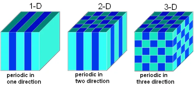
(13) Figure 1.1:. The schematic illustration of one-, two-, and three-dimensional photonic. crystals. Different color represents different dielectric constant.. These artificial structures can be classified systematically by one-dimensional (1D), two-dimensional (2D), and three-dimensional (3D) periodic arrangements of dielectric materials as shown in Fig. 1.1. The basic example of 1-D photonic crystal is distributed Bragg reflectors (DBRs) which consist of alternating layers of material with different dielectric constants in specific direction. Bragg diffraction in these periodic arrangements results in light interference manifested PBG, where certain frequencies of electromagnetic propagation are inhabited. This 1D photonic crystal, therefore, can act as a perfect mirror for light with a frequency within a sharply-defined gap. For example, in the Fig. 1.2, the DBRs are consisted by high and low indices material of 1/4λ thickness and the calculated reflectivity of the structure is with a narrow band gap prohibiting light propagation through the plane between the light wavelengths from 900 to 1070 nm.. 2.
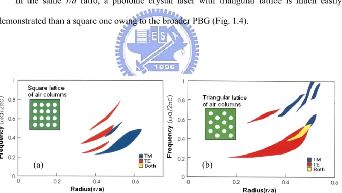
(14) λ GaAs(74 nm) AlAs (82 nm) GaAs AlAs GaAs AlAs GaAs AlAs. Figure 1.2:. 4. A typical calculated reflectance spectrum for the GaAs/AlAs pairs DBR center. at 975nm. The schematic of this DBR structure is shown in right inset.. The 2D photonic crystal, as shown in the Fig. 1.3, can be formed by a periodical arrangement of solid rod in the air or air holes in the high refractive indices substrate. 2D photonic crystal is now being widely studied. In fabrication, the use of E-beam lithography to define pattern is the main stream. And then some dry and wet etching processes are used to realize 2D photonic crystal structure. In 3D photonic crystal fabrication process, chemical self-assembly is mostly used.. And there are many application have been shown as photonic crystal fiber (PCF)、photonic crystal laser、photonic crystal waveguide and LED. With proper design, the medium can expels photons with certain wavelengths and wave vectors. Such a structure acts as an insulator of light, some gap map of such structure are show in Fig. 1.4. The insert shows the photonic crystal design pattern. Typically, we can separate 2D photonic crystal lasers into two different geometry, square lattice [5, 6] and triangular lattice [7, 8]. 3.
(15) (a) Figure 1.3:. (b). The schematic illustration of 2D photonic crystals formed by (a) dielectric rod. and (b) air hole slab. Different color represents different dielectric constant.. In the same r/a ratio, a photonic crystal laser with triangular lattice is much easily demonstrated than a square one owing to the broader PBG (Fig. 1.4).. (a). Figure 1.4:. (b). Gap map for a square (b) triangular lattice of air columns with dielectric. medium with dielectric constant of 11.4. PBGs in a triangular lattice are usually broader than that in square lattice with the same r/a ratio. The light gray region in (b) is a complete band gap which included the PBGs with TM mode and TE mode. (Adopted from reference [4]). 4.
(16) 1.2. Photonic Crystal lasers. So far, we mention about the idea of PBG effect which means standing waves of electromagnetic waves can be formed within a periodic structure whose minimum scale is in the order of wavelength. By introducing point or line defect in the periodic photonic lattice as shown in Fig. 1.5. One can give rise to some localized modes within the band gaps and hence allow people to confine and manipulate the flow of light in these structures. This behavior is analogous to that seen in crystalline semiconductor thereby making photonic crystals excellent candidates for PBG and defect engineering. For above reason, in the past decades, various photonic crystal devices have been proposed and investigated.. The recent notable contributions of PCs to improvement of the existing common semiconductor light sources including replacement of the cleaved laser facets with PCs [9], enhancement of vertical extraction efficiency in LEDs [10], reduction of refractive index in vertical cavity surface-emitting lasers (VCSELs) to improve the optical lateral confinement [11], and so on. When integrated with sub micrometer scale light emitters and detectors, these components could eventually lead to the realization of functional ultra-small high-density photonic integrated circuits [12] and wavelength division multiplexing (WDM) system in communication systems application [13].. 5.
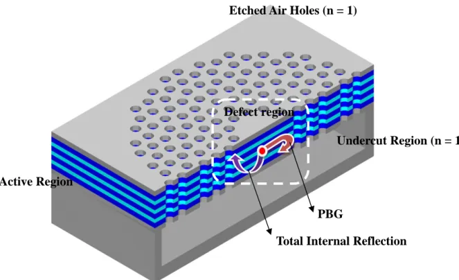
(17) (a). (b). Figure 1.5: (a) A photonic crystal point defect is formed by single or more missing air holes. This is widely used to construct the photonic crystal micro-cavities. (b) A photonic crystal line defect is formed by removing one or more rows of the air holes. This kind of defect has been widely used in low-loss photonic crystal waveguide. 2D photonic crystals with a triangular lattice of air holes in membrane structure [14, 15] have used to study photonic crystal microcavity effects. A microcavity laser with a wide range of tailored modes excitable by the active layer within the cavity can be created by removing several selected air-holes lattice, or modifying the parameters of the inner holes near cavity region [15]. These structures have rather capable of confining light within microcavities with expressive high quality factors as a result of quai-3D light confinement. As the Fig. 1.6 shown, quai-3D light confined with the in-plane confinement provided by the PBG and the vertical confinement by total internal reflection (TIR) provided by the air cladding. But in recent years, there are some different design methods for photonic crystal lattice, such as circular-periodic photonic crystal and quasi-periodic photonic crystal (QPC), to achieve further low-threshold and high quality factor.. 6.
(18) Etched Air Holes (n = 1). Defect region Undercut Region (n = 1) Active Region PBG Total Internal Reflection. Figure 1.6: The scheme of cross section for the photonic crystal microcavity and its optical confinement mechanism.. 1.3 Motivation. Various photonic crystal lasers have been reported with improved properties [16]–[20]. However, most of them are pumped optically. As a candidate for the electrically pumped structure, the introduction of a small post at the center of the cavity is suggested [21]. If a small post is positioned at the intensity minimum of a mode, characteristics of the mode will hardly be changed, and electric current can be injected through this post [22]. Also, it is possible in this structure to select only modes with a node at the post and obtain a better heat sink. As a preliminary step to the electrical pumping, the photonic crystal slab structure with a post is studied with optical pumping.. 7.
(19) As mention before, if a small post is positioned at the intensity minimum of a mode, characteristics of this mode will hardly be changed. In this thesis, we design 12-fold QPC microcavity with whispering gallery mode (WGM). One calculated mode presents zero-order radial WGM profile with azumithal number 6 (W6) mode, as shown in Fig. 1.7, which agrees with the results in Ref. 23. W6 mode is a very potential mode due to its high quality factor [over 200000 (Ref. 24)] contributed to the good consistency with the cavity geometry. More important, its central node with zero field distribution is quite suitable for electrical injection structure. Integrated above characteristic, 12-fold QPC microcavity laser is an ideal candidate for electrical pumping photonic crystal laser. In this thesis, we will focus on the asymmetry 2D photonic crystal structure as a platform for a variety of microcavity lasers. And discuss the effect after the introducing of bottom DBR and central post.. Figure 1.7: The magnetic field mode profile of WGM, with azumithal number 6 (W6 mode), which is calculated by 2D FDTD method.. 8.
(20) 1.4. An overview of this thesis The basic theory of our design, simulation results, procedures of fabrication,. photoluminescence (PL) measurement results and devices analysis were included in the following chapters. The simulation results of asymmetric 12-fold QPC microcavity laser were introduced in chapter 2. Fabrication procedures were demonstrated in chapter 3. And the problems in fabrication were also discussed in detail. In chapter 4, the basic lasing characteristics of 2D photonic crystal lasers are measured by a near-infrared (NIR) micro-photoluminescence (micro-PL) system. Besides, the measurement results were further compared and analyzed.. Chapter 2. Modal Analysis of Asymmetric 12-fold QPC Microcavities. 2.1. Introduction There are two different types of photonic crystal microcavity lasers discussed in this chapter. One is 12-fold QPC microcavity with bottom DBR structure, and the other is 12-fold QPC microcavity with central post. In this thesis, we mostly focus on 12-fold QPC microcavity with central post. The fabrication process of these two structures will be discussed in chapter 3.. At first, we will describe the theory and structure of our devices structure in detail. We use several numerical analysis methods to verify our designs and measurement results. The resonance modes in microcavity and its mode profile were calculated by finite-different 9.
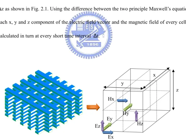
(21) time-domain (FDTD) method. The simple theory of simulation will be discussed and simulated result will show in the latter of this chapter.. 2.2. Simulation method. 2.2.1. Finite Difference Time Domain Method FDTD is a method that numerically calculates the space and time changes in the electromagnetic fields of light. By this technique, an analytical finite space including the objective structure is divided into small cubic cells called Yee’s cells with edges of Δx =Δy = Δz as shown in Fig. 2.1. Using the difference between the two principle Maxwell’s equations, each x, y and z component of the electric field vector and the magnetic field of every cells is calculated in turn at every short time interval Δt.. x y z Hx. Ey Ez Ex Figure 2.1: Calculation model and Yee’s cell. 10. Hy Hz.
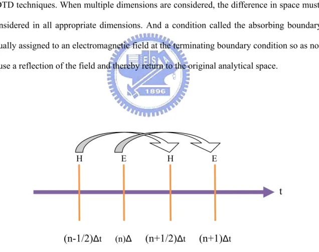
(22) When we are examining the differential from Maxwell’s equation, it can be seen that the time derivate of the electric field is relate to the Curl of the magnetic field. As we know, the change of the electric field is dependent on the change of the magnetic field in the space. So is similar to magnetic field. This results in the basic FDTD equation means the new value of the electric field is associated with the old value of the electric field and the difference in the old value of the magnetic field on either side of the electric field point in space. We could use Fig. 2.2 to represent the relationship between the electric field and magnetic field. This can be simplified to state that the change in the E field (the time derivative) is dependent on the change in the H field across space (the Curl). This description holds true for 1D, 2D, and 3D FDTD techniques. When multiple dimensions are considered, the difference in space must be considered in all appropriate dimensions. And a condition called the absorbing boundary is usually assigned to an electromagnetic field at the terminating boundary condition so as not to cause a reflection of the field and thereby return to the original analytical space.. H. E. H. E. t. (n-1/2)Δt. (n)Δ. (n+1/2)Δt. (n+1)Δt. v v Figure 2.2: Temporal division of E and H components. 11.
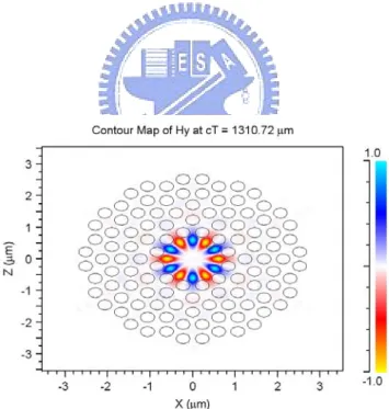
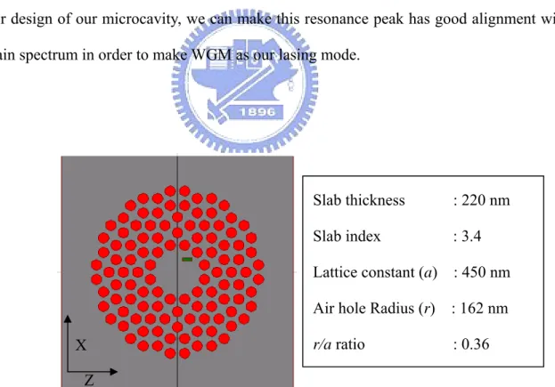
(23) 2.2.2. Mode Analysis by 3D FDTD Method In the purpose to analysis lasing modes in our structures, we apply 3D FDTD method to calculate the resonance modes spectrum and their profiles. In this section, we will simply describe our simulation method and show how to simulate the resonance mode spectrum and its lasing mode profile.. 12-fold QPC microcavity scheme with a=450 and r/a=0.36 is show in Fig. 2.3. With proper setting of slab index (3.4)、slab thickness (220 nm) and cavity formation, we can approach the real case in our microcavity. A calculated result of resonance mode spectrum is show in Fig. 2.4, several resonance peaks are observed. The peak at 1375nm is WGM. With proper design of our microcavity, we can make this resonance peak has good alignment with the gain spectrum in order to make WGM as our lasing mode.. X. Slab thickness. : 220 nm. Slab index. : 3.4. Lattice constant (a). : 450 nm. Air hole Radius (r). : 162 nm. r/a ratio. : 0.36. Z Figure 2.3: The scheme and simulation setup of 12-fold QPC microcavity. The circles and square denote the air holes and the slab. The smaller rectangular in microcavity is the time monitor.. 12.
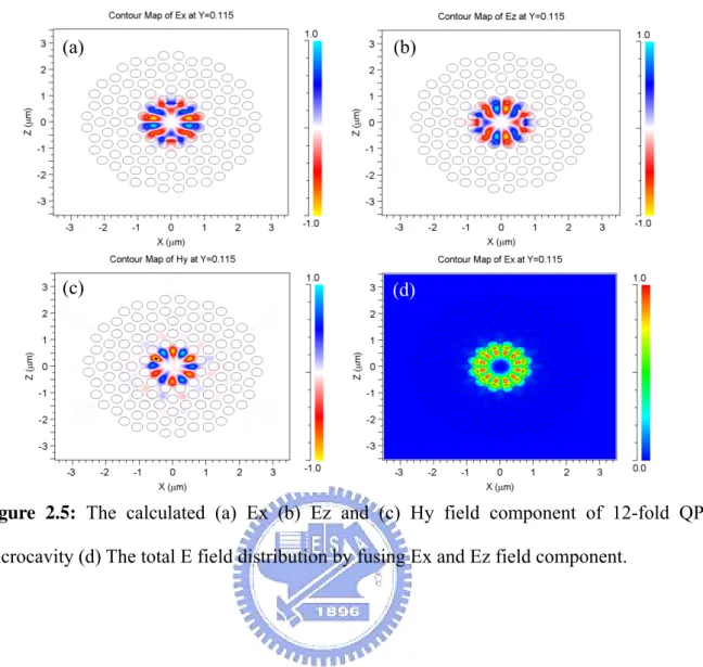
(24) WGM. Figure 2.4: The calculated spectrum of resonance modes in 12-fold QPC microcavity with lattice constant of 450 nm and r/a ratio of 0.36 is show.. There are three kinds of field element distribution we can get after the calculation which are Y component of magnetic field, X and Z component of electric field. Thus, we can calculate the total electric field and analyze the mode characteristic. From Fig. 2.5, we can clear observe the WGM with a zero mode distribution in both electric field and magnetic field and the standing wave is formed in the nearest air holes of a micro-gear like cavity. This well-confined WGM profile in magnetic field with azimuthal number six of the modified microcavity is obtain. And the numbers of lobes are match with the number of gears as shown in Fig.2.5.. 13.
(25) (a). (b). (c). (d). Figure 2.5: The calculated (a) Ex (b) Ez and (c) Hy field component of 12-fold QPC microcavity (d) The total E field distribution by fusing Ex and Ez field component.. And for graphical illustration of the vertical loss, the momentum space intensity distribution [25] obtained by Fast Fourier Transforming (FFT), the in-plane field 2. 2. ( FT ( Ex ) + FT ( Ez ) ) is calculated. From the in-plane momentum conservation rule, only. plane-wave components inside a light-cone [k x2 + k y2 = (ω / c)2 ] can couple with propagation modes. As can be seen from the momentum space intensity distributions of the WGM in Fig. 2.6, the resolution is limited by the setting of FDTD grid size. The major fraction of the resonant photons lives outside the light-cone, which implies an efficient index confinement mechanism. 14.
(26) Figure 2.6: Electric-field distribution of the WGM in Momentum space in 12-fold QPC microcavity. The dotted circle represents the light-cone. The major fraction of the plane-wave components lies outside the light-line, which implies the efficient index confinement mechanism.. 2.3. Device Structure. 2.3.1. 12-fold QPC Microcavity with Bottom DBR. In our asymmetry structures design, the lower cladding layer of MQWs slab is a DBR substrate but the air cladding layer as in symmetry membrane structures as shown in Fig.2.7. For this asymmetry structures, which can improve the thermal effect produced from optical pumping on the membrane structure microcavity and provide the better confined of light in vertical direction. The application of DBR structure was widely used in VCSEL. And following the concept in VCSEL, Our DBR structure is composed of 22 pairs of GaAs/Al0.9Ga0.1As layer and high reflectivity region lays wavelength from 1450 to 1600 as shown in Fig. 2.8. 15.
(27) MQWs DBR. Figure 2.7: The side view illustration of 12-fold QPC microcavity with DBR substrate.. Norm. Reflectivity. 1.0. 0.8. 0.6. 0.4 1000 1100 1200 1300 1400 1500 1600 1700. wavelength (nm). Figure 2.8: The measured high reflectivity of DBR from 1450 to 1600 nm.. 16.
(28) 2.3.2.. 2D Photonic Crystal Cavity Laser With Central-Post. Central-Post structure was first reported by using traditional triangular photonic crystal D3 microcavity [21]. It is possible in this structure to select only modes with a node at the post and obtain a better heat sink. As a preliminary step to the electrical pumping, the photonic crystal slab structure with a post is studied with optical pumping. Fig. 2.9 shows our 12-fold QPC microcavity laser with central post. In the chapter 4, we will show how to construct a post just under the microcavity.. The reason why we choose 12-fold QPCl as our pattern design is that high quality factor WGM can be sustained in 12-fold QPC microcavit. As mention before, if a central post is positioned at the intensity minimum of a mode, characteristics of the mode will hardly be changed, and electric current can be injected through this post [26].. 12-fold QPC microcavity MQWs membrane Central Post. Figure 2.9: The scheme of 12-fold QPC microcavity laser with central post.. 17.
(29) 2.4. Simulation Result. 2.4.1. Modal Analysis of 12-fold QPC microcavity with Bottom DBR. As mention in previous section, in order to improve the thermal effects produced from optical pumping on the membrane structure and provide the better confinement of light in vertical direction, we design an asymmetry structures, the lower air cladding layer is replaced by a DBR substrate In this section we will use 3D FDTD to calculate the influence of the lasing mode profile after introducing bottom DBR. The scheme of our device structure is show in Fig. 2.10, different cut directions of contour map are provided; we can see the difference between three kinds of bottom DBR structures which is the depth of our defined 12-fold QPC air hole and the number of our DBR pairs.. (a). (b). (c). (d). Figure 2.10: The contour map of index profile. (a) XZ plane of 12-fold QPC microcavity. PC pattern transform to (b)MQWs, (c)four pairs of DBR layer, and (d)one has four more DBR pairs under the PC patterned MQWS and DBR layer. 18.
(30) After calculation of resonance mode spectrum, we find that no resonance mode is observed in the PC pattern only transform to MQW, as shown in Fig. 2.11(a). In contrast, only the pattern transform into DBR layer will have resonance mode as shown in Fig. 2.11(b) (c).. (a). (b). (c). Figure 2.11: Resonance mode spectra of PC pattern transform to (a)MQWs, (b) four pairs of DBR layer, and (c)one has four more DBR pairs under the PC patterned MQWS and DBR layer.. There are two possible reasons, one is in-plane energy loss and the other is vertical loss. In-plane loss depends on 12-fold QPC PBG effect, so the problem is the bottom DBR really reflects the downward light or the light did not feel the existence of bottom DBR.. In order to investigate the vertical loss, the momentum space intensity distribution is calculated. As one can see from the momentum space intensity distributions of the resonant modes, if the major components live outside the light-cone, it implies an efficient index confinement mechanism. In Fig. 2.12, we compare the momentum space intensity distribution of three kinds of bottom DBR structure to each other.. 19.
(31) (a). (b). (c). Figure 2.12: The momentum space intensity distribution of PC pattern only transformed into (a) MQWs, (b) four pairs of DBR layer and (c) four more no patterned DBR pairs under the PC patterned MQWS and four pairs of patterned DBR.. We can find out that if PC pattern only transform into MQWs layer the loss is huge. In contrast, if PC pattern transform pg deep into bottom DBR, the vertical loss can be improved. By increasing the depth into bottom DBR, the component inside the light cone can be reduced as shown in Fig. 2.12 (c), i.e. the vertical loss is further improved. However, the component of momentum space intensity distribution inside the light cone is very large compared with that of the membranes structure as shown in Fig. 2.6. This implies the quality factor of this structure would be smaller than that of membranes structure. This result is not what we expect, the bottom DBR does not give a well confinement of light and achieve a high reflectivity to ensure radiations from the top surface. This may caused by the direct contact of our MQWs and bottom DBR. As a result, promise solution of the tradeoff between vertical emission enhancement and optical loss should be proposed. The scheme of modified structure is show in Fig. 2.13. An additional air-gap is used between the DBR and the MQWs in order to compensate the optical loss.. 20.
(32) MQWs Air-Gap DBR. Figure 2.13: The scheme of 12-fold QPC microcavity with bottom DBR and air-gap.. We also use 3D FDTD to calculate the influence of the lasing mode profile by introduce the different air-gap size from 0.125 λ to 0.5 λ . Their momentum space intensity distributions are show in Fig. 2.14. When the size of the air gap becomes smaller, the loss of the field energy becomes large. By the theoretical studies, the different air-gap size will influence the far field pattern without change the near field pattern. The quality factor will decrease when the distance between MQWs and bottom DBR become smaller. The vertical enhancement condition is reported to be 2d=mλ, where d is the air-gap size and m is integral [27].. 21.
(33) (a). (b). (c). (d). Figure 2.14: The momentum space intensity distributions of (a) traditional membrane structure and structures with air-gap distance of (b)0.125λ (c)0.25λ (d) 0.5λ.. 2.4.2. Modal Analysis of 12-fold QPC microcavity with Bottom DBR. As a candidate for the electrically pumped structure, a post is designed to place at the center of the microcavity with WGM, and then electric current can be injected through this post. In this section, as a preliminary step, the photonic crystal microcavity with a post is studied with 3D FDTD for different radius of post. At first, we design a 12-fold QPC microcavity with a central air hole to approximate the effect of microcavity with central post. We use this structure to pre-study the characteristic of WGM. By change the radius of the central air hole, we can estimate the energy distribution of WGM and to design the size of central post. The result is show in Fig. 2.15, when the radius is bigger than 2.8r, i.e. r = air hole radius; the central air hole will cause the WGM resonance will be distoryed. 22.
(34) X. (a). X. Z. (b) Z. Figure 2.15: The total electric field distribution of 12-fold QPC microcavity with (a) 2.0 r and (b) 3.0 r radius central air hole. When central air hole radius is bigger than 2.8 r, the WGM resonance will be distoryed. The central circle denotes the central air hole.. According to above results, we continue to calculate 12-fold QPC microcavity with central post by 3D FDTD simulation, the CAD design are shown in Fig. 2.16. We can observe the graded-index layer between air and slab layer. This phenomenon is caused by the setting of grid size. To solve this problem, we can diminish the grid size, but would increase the simulation time, so we would set the proper grid size to achieve an acceptable simulation result. After the simulation, we can find out that in post structure, the radius can be add to 3.6 r without conspicuousness influence the mode profile of WGM. This conclusion does not well accordance with the central air hole, these may be explained by poynting theorem. But this is good for the post radius to become large in order to reduce the resistance when we play the central post as a conducting wire to inject electric current.. 23.
(35) Figure 2.16: The simulation setup of our central post structure in (a) XZ plane contour map and (b) XY plane contour map of index profile.. In order to do more detail analyze, we will illustrate the change of total E field distribution and the momentum space intensity distributions cause by difference central post size (Fig. 2.17). We change the post size from 1.5r to 3.7r and according to the simulation result to deduction that if the post radius is bigger than 3.6r, the plane-wave component inside a light-cone becomes large and these field element would couple with propagation mode.. Ⅰ. Ⅱ. Ⅲ. (a) The membrane structure. 24.
(36) Ⅰ. Ⅱ. Ⅲ. (b) When the radius of central post is 1.5r Ⅰ. Ⅱ. Ⅲ. (c) When the radius of central post is 3.0r Ⅰ. Ⅱ. Ⅲ. (d) When the radius of central post is 3.5r. Figure 2.17: The (Ⅰ) electric-field distribution in momentum space and (Ⅱ) XZ plane and (Ⅲ) XY plane of total E field. We can observe that the energy will go through the post when the post radius is 3.5r and lead to the increase of component inside the light cone. If we continue to increase the radius of the post, for example, bigger than 3.6r, the WGM will no longer exist.. 25.
(37) Moreover, it is also possible to select only modes with a central node. This can be proven by calculating its resonance spectrum as shown in Fig 2.18. When a central post introduced, the monopole will disappear in the resonance spectrum to achieve side mode reduction. This is because the mode intensity of monopole is concentrated at the center, so it will be abolish when introduce a small post under the center of microcavity. (b). (a) monopole. (c). Figure 2.18: (a) The simulated resonance spectrum of membrane structure and central post structure. In this diagram, we can observe that the monopole mode is reduced in central post structure. From the (b)XZ plane and (c) XY plane total electric field of monopole, we can clearly observe that the mode intensity of monopole is mostly concentrated at the center.. 26.
(38) 2.5 Conclusion. We have shows that the slab resonant mode profile with bottom DBR and even more we introduce a air gap between bottom DBR in order to improve the bottom side confinement effect. And we calculate the influence to the WGM when a central post is introduced. To minimization the energy lost cause by central post, the radius of the post most control under 3.4r, and those to minimize the resistance when we play the central post as a conducting wire to inject electric current.. Chapter 3. Fabrication Process of Asymmetric 12-fold QPC Microcavities. 3.1. Introduction The basic design principles and simulation results of 12-fold QPC microcavity with bottom DBR and 12-fold QPC microcavity with central post have been introduced in chapter 2. In this chapter, the fabrication procedures of two different structures of 12-fold QPC microcavities will be discussed in detail and the problems during the process will also be presented.. 3.2. Fabrication of 12-fold QPC Microcavity With Bottom DBR. 3.2.1. Preparation for Wafer Bonding. There will be unbounded area if the wafer surface has particles and defects [28]. To 27.
(39) prevent these, before pre-bonding in room temperature, we clean the sample’s surface at first. Moreover, in order to prevent the thermal stress between interface; some channel lines must be transferred on the InP cap layer before pre-bonding.. For MQWs/DBR pairs, the channel pattern must be parallel to the <01-1> direction of InP substrate otherwise the cap layer of MQWs will be removed during the wet etch process as shown in Fig. 3.2(b). The gap size is estimate to be 33.3 nm which is close to the thickness of our InP cap layer. No enhancement will be observed if there is a gap between InP and DBR as shown in Fig. 3.2 (b). In Fig. 3.1 (a), pattern parallel to the <01-1> direction has no air gap between bonding interface. The measurement result of sample without gap shows the enhancement centered at 1550 nm due to the bottom DBR effect and the other sample with gap shows nothing. In Fig. 3.2 (a) the “1” data line have week enhancement compare to “2” data line, this is because the quality of bonding interface was not good enough in the edge of the bonding sample due to the thermal stress. This phenomenon can be used to verify the quality of our bonding sample.. (a). (b). 291nm. 212.5 nmnm 245.8nm. Figure 3.1: The side view SEM picture of channel pattern (a) parallel and (b) vertical to the <01-1> direction of InP substrate.. 28.
(40) (a). 1.0. 2 11. Normalize intensity. 0.8. 0.6. 0.4. 0.4. 0.2. 0.0. 0.0 1300. 1350. 1400. 1450. 1500. 1550. 1600. 1650. 1250. 1300. Wavelength (nm). Figure 3.2:. 2 1. 0.6. 0.2. 1250. (b). 0.8. Normalize intensity. 1.0. 1350. 1400. 1450. 1500. 1550. 1600. 1650. Wavelength (nm). The measurement result of MQWs/DBR with channel pattern (a) parallel and (b). vertical to the <01-1> direction of InP substrate. 3.2.2. Process for Direct Wafer Bonding. Surface treatments for all samples are still required before the bonding process. The sample and DBR wafer were cleaned in the acetone solution for 5 minutes, then use D.I. Water to rinse for 5 minutes. After the cleaning process, two wafers were stick together face to face in the D.I. water without contact to the surrounding air. Then use N2 to drying the stuck sample and checking two wafers were stuck by Van der Waals force. As the Fig. 3.3 shown, the stuck sample was clipped on the wafer bonding fixture. The different thermal expansion coefficient of stainless steel and molybdenum material is the main principle of wafer bonding process. Owing to the different thermal expansion coefficient, high pressure was formed at high temperature.. 29.
(41) Molybdenum Screw. Molybdenum Nut. Stainless Steel. Two wafers for Bonding. Graphite Plate. Figure 3.3: The scheme of wafer bonding fixture.. At last, wafer bonding fixture was put into the center of the furnace as shown in Fig. 3.4. The sample is heated to 600℃ in 90 minutes and holds the temperature for 60 minutes. Finally, the annealing process was that let the furnace cool down naturally to room temperature. Because of the high temperature and high pressure be occurred in furnace, the interface of two wafers would have a chemical reaction to form the atomic covalent bond. Furthermore, the function of graphite plate is to prevent the bonding reaction between wafer and stainless steel. After the proper time for annealing, two wafers were bonded together.. Furnace Gauge. Pump. PID controller. Figure 3.4:. N2 H2. A illustration of the wafer bonding system. 30.
(42) After the wafer w bondinng process, the upper layer of InP substrate w will be remo oved by wett etchiing process. The bondded sample was fixed by clips annd put into a HCl : H2O = 4 : 1 soluttion for 30 minutes m to remove r the InP substraate. After thhat, the smooth and glo ossy MQWss with DBR substrate wafer were demoonstrated ass shown in Fig. 3.5; thhe surface of bondingg sampple is roughh because thhe releases of thermal stress on thhe bonding interface. And A in Fig.. 3.5 (b) ( we can see s the bonnding interfaace of MQW Ws/DBR paairs, and thee MQWs plus InP capp layerr is about 2445nm.. Bonding sam B mple’s su urface. ~ 245 nm ~ 355 nm m nding Esstimate bon in nterface ~ 110 nm m (aa). (b). Figu ure 3.5: (a) Side S view SEM S picturee of the bon nding sample and its esttimated (b) bonding interface.. 3 3.2.3. Ph hotonic Crystal C Paattern Deffinition an nd Transffer. We depositted a 300 nm n thickness Si3N4 lay yer as an etcch mask by PECVD prrocess. Thee thickker Si3N4 thaan 140 nm is i owing to against the longer dry etching tim me. A 300 nm m thicknesss of PM MMA layerr was spun on Si3N4 layer, l and th he PC micrrocavity pattterns were written byy EBL system. Foor transferriing PC pattterns into MQWs M layeer, the ICP/R RIE system m was used.. The Si3N4 hard mask was etched by CHF C 3/O2 mixed m gas inn RIE modee dry etching, and thenn 31.
(43) CH4/Cl2/H2 mixed gas is used to transfer the patterns into MQWs at 150℃ for 40 seconds in ICP etching mode. Then, the Ar/SiCl4 mixed gas is used to transfer the PC patters into DBR ubstrate at 20℃ for 4 minutes in ICP etching mode. The PC lasers with bottom DBR structure was demonstrated after removing the residual hard mask on the MQWs. In Fig. 3.6, there are overviews of fabrication processes of 2D photonic crystal wafer bonding structure lasers.. InP. MQWs. Channels Transfer. PR. DBR. Si3N4. PMMA. InGaAs. Photoresist Coating. Channels Define. Remove PR & Clean Surface. Wafer Pre-Bonding. Remove Substrate. Si3N4 Deposit. PMMA Coating. Electron-Beam Define. Patterns Transfer. Remove PMMA. Pattern Transfer. Remove Si3N4. Wafer Bonding. Figure 3.6: An overview of fabrication processes of bottom DBR structure. 32.
(44) 3.3. Fabricatiion Resullts & Con nclusion. 3 3.3.1. Bon nding with InP / DB BR Interfface. We have faabricated a well designned 12-fold d QPC micrrocavity witth bottom DBR. D Afterr the definition d off PC patterss and transfform by EB BL system and a ICP/RIE E dry etching process,, the 12-fold 1 QPC C microcaviity with botttom DBR is i formed byy remove suurface hard d mask. Fig.. 3.7 shows SEM pictures off our fabricaated device.. (b). (a). 3 pairss DBR. ure 3.7: Figu. T (a) top view and (b) cross section SE The EM picturess of the 12 2-fold QPC C. microocavity withh bottom DBR.. 3 3.3.2. Bon nding with SiO2 / SiO S 2 Inteerface. The differeence of fabrrication proocess betweeen InP / DBR pairs annd SiO2 / SiO S 2 pairs iss that after the chhannel patteern transforrmed, we deeposit SiO2 as sacrificeed layer on n surface off both samples. And A the suubsequencee fabrications for bonnding are aall the sam me. But wee 33.
(45) encounter a problem during the direct wafer bonding process to combine the double side SiO2 layer. At first, we test two kind of deposit method, one is SAMCO PD-220 plasma enhanced chemical vapor deposition in NDL 10k class clean room and the other is furnace in NDL 10 class clean room. After the direct bonding, only the furnace one combines successfully, the layer deposit by PECVD did not work. In order to analyze this result, we use Atomic Force Microscopy (AFM) to study the surface of both samples as shown in Fig. 3.8. The roughness of SiO2 deposit by PECVD is about 10 times larger than deposit by furnace. The roughness of sample surface will cause the particles to hide inside the surface defects and cause the bubble or other effect to damage the bonding interface.. (a). (b). Figure 3.8: The surface roughness of SiO2 deposited by (a) furnace and (b) PECVE. The SiO2 surface roughness by furnace one is 0.266 nm and by PECVD is 2.740 nm. 34.
(46) 3.4. Fabrication of 12-fold QPC Microcavity With Central-Post. 3.4.1. Epitaxial Structure and Dielectric Material Deposition. At first, the epitaxial structure illustrated in Fig. 3.9 is prepared. It consists of four 10 nm 0.85% compressively strained InGaAsP quantum wells (QWs) which are separated by three 20 nm unstrained InGaAsP barrier layers. It has been confirmed that the PL spectrum of the QWs (Fig. 2.1(b)) is centered at 1550 nm with 200 nm span. The QWs is grown on InP substrate by metal organic chemical vapor deposition (MOCVD) and then a 60 nm InP cap layer is deposited on it for protecting the QWs during a series of dry etching processes. In fabrication, at first, a 140 nm thick Si3N4 layer served as a hard mask is deposited by SAMCO PD-220 plasma-enhanced chemical vapor deposition (PECVD) process. The SiH4/NH3/N2 gases mixture are used to deposit dielectric hard mask on 300℃ substrate at 35W plasma power in 100 Pa pressure. The Si3N4 thickness of 140 nm can stand for the whole dry etch process when achieving the depth into our wafer about 800 nm.. 60nm InP Cap Four 10nm 0.85% compressively strained InGaAsP QWs ( Eλ ~1.55μm) with three 20nm unstrained InGaAsP Barriers ( E g ~1.22μm). 57.5 nm InGaAsP barriers InP Substrate Figure 3.9:. The scheme of epitaxial structure of InP/InGaAsP MQWs. The thickness of. active region is about 220 nm.. 35.
(47) 3.4.2. Photonic Crystal Patterns Definition and Dry-Etching Processes. At first, the QPC pattern is designed by using CAD tools. And then we load this file into Nanometer Pattern Generation System (NPGS) system. Then photonic crystal patterns were defined by JEOL JSM-6500F electron-beam lithography (EBL) system. The EBL system is a field-emission scanning electron microscope, which employs a schmasky type fields-emission gun for the electron source and state-of-the-art computer technology for high-resolution image observation. Before EBL, an A5 polymethylmethacrylate (PMMA) resist layer is spin-coated on the wafer after previous dielectric deposition process. The PMMA thickness is 300 nm.. After defining QPC patterns by EBL system, the pattern will be transferred by the following processes. In transferring patterns, Oxford Instruments Plasma Technology Plasma lab 100 inductively coupled plasma / reactive ion etching (ICP/RIE) system is used. At first, the sample is etched by O2 plasma in order to clean the residual PMMA in air holes. And then the Si3N4 hard mask is etched by CHF3/O2 mixed gas in RIE mode dry etching. The Si3N4 etching environment recipes are 150W RF power and 55 mTorr at 20℃ with CHF3 and O2 gas flow rate of 5 sccm and 50 sccm, respectively. The etching rate in CHF3/O2 mixed gas is about 1.5 nm/s in average and the selectivity etching ratio to PMMA is 8. After transferring the pattern into Si3N4 layer, we use O2 plasma to remove the survival PMMA layer. And then the pattern transforming into InP/InGaAsP MQWs layer is achieved by H2/CH4/Cl2 mixed gas in ICP mode dry etching. The MQWs etching environment recipes are 73W RF power, 1000W ICP power, and 4 mTorr at 150℃ with H2、CH4 and Cl2 gas flow pressure of 0.8, 0.4, and 0.3 mTorr, respectively. The etching rate in H2/CH4/Cl2 mixed gas is about 5.5 nm/s in average and the selectivity etching ratio to Si3N4 is 6. After a serious of dry etches process mentioned above, the PC patterns have already been transferred onto the QWs.. 36.
(48) 3.4.3. Construct of Central Post Structure. In order to form the central-post structure, the InP substrate below the MQWs should be removed and leave only a post under the center of our microcavity. This can be achieve by immersion the sample into a mixture solution with HCl : H2O = 3 : 1 at 2.5℃ for about 1 minutes, and then the solution goes through the drilled holes to form a small post. This process also removes 60 nm InP cap layer and smoothes the surface and the sidewall of the air holes.. In general photonic crystal patterns, for example, triangular lattice photonic crystal, the CAD design must includes windows to break the InP etching stop plane and achieve membrane structure [29]. However, the etching stop plane can be easily broken due to the lattice structure of 12-fold QPC and the undercut will form. As a result, it is unnecessary to define the windows in our CAD file. Fig. 3.10 shows the SEM picture of our sample after wet etch process. We find that the undercut of outer region of QPC is not formed caused by smaller air-hole in the outer region due to proximity effect during EBL process. Also, in the same sample with larger r/a ratio, the membrane structure has been formed under the same wet-etching time. This also indicates the sensitivity of wet etching time in different r/a ratio pattern.. 37.
(49) (a). b) (b. Figu ure 3.10: Thhe top view w SEM pictuure of 12-fo old QPC miicrocavity w with differen nt r/a ratio.. (a) The T undercuut of outer laayer is not formed f wheen the r/a raatio is smalll. (b) In con ntrast, underr the same wet-etcching time, the membrrane structurre has been formed witth larger r/a a ratio.. In order to solve this problem, we w re-design n a new CA AD file by eenlarge the air a holes off outerr three layerrs to be 1.33 time of deesigned r/a ratio as shoown in Fig. 3.11. This design willl produuce differennt etching rate r betweenn inner and outer regioons and promote the po ost formingg at thee center of microcavity m y.. Ⅰ. Ⅱ. ure 3.11: Thhe modifiedd CAD file of QPC microcavity. The T r/a ratio of outer three t layerss Figu (regiion II) is 1.33 time of thaat in region I. 38.
(50) (b). (a). (c). Figure 3.12: (a)The top view SEM picture of fabricated sample.. A 12-fold QPC. microcavity with central post. (b) The parallelogram shape of central post. (c) A fabricated 12-fold QPC microcavity membrane with crashed outer region due to the over dosage of EBL is supported by the central post.. Fig. 3.12 (a) shows the top-view SEM picture of fabricated 12-fold QPC microcavity with central post. The parallelogram shape of central post is observed from the SEM picture in Fig. 3.12 (b). This asymmetric shape is caused by the anisotropic etching rate of InP material. In Fig. 3.12 (c), a fabricated 12-fold QPC microcavity membrane with crashed outer region due to the over dosage of EBL is supported by the central post. This structure is very fragile because the absence of outer connections. To solve this problem, we design the other two CAD files and the first one is show in Fig. 3.13. This design will produce contacted bridge to connect membrane and wafer to form a stronger central post structure. Fig. 3.14 shows the top-view SEM picture of fabricated device with contacted bridge between QPC membrane and the wafer. Moreover, we can shift the larger air holes away from the other air hole to make the contacted bridge stronger. 39.
(51) Ⅰ Ⅱ Contacct Bridge. Ⅲ. Figu ure 3.13: The T CAD design d with contacted bridge. Thhe r/a ratio of outer three layerss (regiion II) are 1.2 time of thhat in regioon I. Some air a holes aree replaced bby larger onees in regionn III too produce thhe contact bridge b betw ween membrrane and waafer withouut affecting the etchingg rate of o outer reggion obvioussly.. Over dosage crashed regionn. Centrral post. Contaact bridge. ure 3.14: Thhe top view w SEM pictture of 12-ffold QPC microcavity m Figu with contacted bridgee betw ween QPC membrane m annd wafer. The T inset piccture is the zoom-in z topp-view SEM M picture off 12-foold QPC miicrocavity. The T circulaar shadow att the cavityy center indiicates the fo ormation off the central c post. 40.
(52) Fig. 3.15 shhows the otther CAD design. d The outer threee layers are replacing by b air holess with alternative radius. Thiis design caan prevent the t crash caaused by ovver dosage during d EBL L proceess at outerr three layerrs and proviide enough etching ratee to form thhe central post p withoutt the fail f of unddercut in thhe outer reggion. Fig. 3.16 shows the top vview SEM picture off correesponded faabricated device.. Figu ure 3.15: Thhe CAD design with alternative a air a holes. Thhe outer thrree layers are a replacedd by air holes with alternatee radius. Thhe distance between tw wo differennt radius airr holes cann produuce enoughh tolerance for f over dossage and preevent membbrane from ccrashing.. Ceentral post. ure 3.16: Thhe top view w SEM pictture of fabrricated micrrocavity witth alternativ ve air-hole.. Figu The inset picturre is the zooom-in topp-view SEM M picture of 12-fold Q QPC microccavity. Thee circuular shadow w at the cavitty center inddicates the formation f o the centraal post. of 41.
(53) (a). (b). 1.19μm 1.5μm 0.776μm. Figure 3.17: The (a) top-view and (b) side-view SEM picture of 12-fold QPC microcavity with central post. The diameter of top and root of the central post are estimated to be 1.19μm and 0.776μm. And the gap between membrane and substrate is estimate to be 1.5μm.. From the top view SEM picture, the circular shadow can be used to estimate the diameter of central post. From Fig. 3.17 (a), the circular shadow is estimate to be 0.84μm in diameter. From the direct measurement in side-view SEM picture in Fig. 3.17 (b), the diameter of central post is estimated to be 1.19μm. As a result, there is about 30 % inaccuracy when we estimate post size from the circular shadow.. However, when we reduce the radius of central post, the circular shadow will disappear. This does not mean the post is no longer under the cavity. The shadow is caused by the different charge distribution in the cavity region and the interface with the central post. However, when the post size reduces, this charge distribution difference will become difficult to observe, i.e. the shadow is difficult to observe and judge the existence of the central post. Thus, to confirm the existence of the central post, the side-view or tilted-view SEM pictures are necessary.. 42.
(54) As shown in Fig. 3.18 (b), there is no shadow observed in the microcavity region, but the post can be clearly observed from a tilted-view SEM picture. The smaller post size can only be estimated from the tilted-view SEM picture. We can first measure the angle of the post. By the diameter estimation at arbitrary point, we can calculate the diameter at the interface of the central post.. Figure 3.18: The tilted-view SEM picture of 12-fold QPC microcavity with the central post. (a) The circular shadow can be clearly observed in the microcavity region when the diameter of the central post is large. (b) However, the circular shadow cannot be observed in the microcavity region when the diameter of the central post is small.. 3.5 Conclusion. We have fabricated a well design 12-fold QPC microcavity with the central post. After the definition of PC patters and transform by EBL system and ICP/RIE dry etching process, the 12-fold QPC microcavity with central post is formed by HCl wet-etching. The central post size can be controlled by different immersed time. Fig. 3.19 shows an overview of fabrication process to summarize the fabrication process. 43.
(55) Electron-Beam Define. Si3N4 Deposit. PMMA Coating. Patterns Transfer & Remove PMMA. Pattern Transfer & Remove Si3N4. Construct of Central Post Structure Figure 3.19: An overview of fabrication processes of 12-fold QPC microcavity with the central post.. 44.
(56) Chapter 4. Measurement Results. 4.1. Introduction. In order to measure our epitaxial materials and characterize the fabricated 2D photonic crystal microcavity lasers with central post, a NIR micro-PL system with sub micrometer scale resolution in space and sub nanometer scale resolution in spectrum is used. The simple configuration of the micro-PL system is show in Fig. 4.1.. Optical Spectrum Analyzer TTL Diode Laser Multi-Port ps Function Generator CCD. NIR High-Speed Power Detector. Figure 4.1: The set-up of our NIR micro-PL system. 45.
(57) In this system, an 845 nm TTL laser is used as the pump source. This TTL laser can be used in pulse operation and continuous-wave (CW) operation by switching a function generator. The pump beam is reflected by a 50/50 beam splitter into a 50x long working distance NIR objective lens with numerical aperture of 0.5. The 48% reflection in angle 45° of the splitter for 845 nm wavelength is confirmed. And the pump beam is focused to a spot-size with 2 μm in diameter by the objective lens. The light emitted from the microcavity is collected by the same objective lens. We use a collective lens to feed the output signal into a multi-mode fiber, and then the signal is detected by the spectrum analyzer, Ando AQ-6315A, with 0.05 nm resolution. All of the following measurement results were estimated by this micro-PL system.. 4.2.. Basic Lasing Characteristics. In this section, we will show some basic characteristics of 12-fold QPC microcavity with central post including lasing spectrum, light-in light-out (L-L) curve, mode polarization, and so on. All measurements are done at room temperature by our micro-PL system. 4.2.1. Measurement Results from Central Post Structures. The well fabricated devices are optically pumped by 845 nm TTL laser with 0.5 % duty cycle at 0.2MHz repetition rate at room temperature. The influence of the existence of central post will be clearly understood by comparing the lasing characteristics of fabricated microcavities with and without central post with each other. As a result, these two kind of fabricated 12-fold D2 microcavities with the same lattice constant and the slightly different hole-radius are measured in order to make a comparison. The lasing actions are observed from the 12-fold QPC microcavities with and without 46.
(58) central post. At first, the typical near and above threshold lasing spectra of 12-fold QPC microcavity without central post are shown in Fig. 4.2. The lasing wavelength is 1582.6 nm and full-width half-maximum (FWHM) is 0.17 nm. The side-mode suppression-ratio (SMSR) is about 25.5dB. The inset of Fig. 4.2 indicates near-threshold lasing spectrum. The typical lasing spectrua near and above threshold of 12-fold QPC microcavity with central post are shown in Fig. 4.3 (a). The lasing wavelength is 1589.5 nm and its FWHM is 0.2 nm. The SMSR is about 10 dB in this lasing spectrum. Also, in Fig. 4.3 (b), we shows a side-view SEM picture of the 12-fold microcavity with central post. From the SEM picture, one can see that a central post under the microcavity is achieved. The size of the post at the interface between the microcavity and itself is estimated to be 95nm in radius.. From the measured results, the existence of the central post induce the red shift of lasing wavelength about 6.92nm which can be seen by comparing two lasing spectra. The quality factor is reduced by the introducing of the central post. The estimated quality factor of membrane structure is about 9300 and that of cavity with central post is decreased to 7900. Reduction of the quality factor is because that the vertical confinement might be influenced by the existence of central post which has been investigated theoretically in Chapter 2.4.2. (See Fig. 2.18). 47.
(59) 0.17 nm 1582.6 nm. Figure 4.2:. The typical lasing spectra near and above threshold of 12-fold QPC microcavity. laser. The lasing wavelength is 1582.6 nm and the inset indicates the near-threshold lasing spectrum which the FWHM is estimated to be 0.17 nm.. 0.20 nm 1589.5 nm. (a). Figure 4.3:. (b). (a) The typical lasing spectra near and above threshold of 12-fold QPC. microcavity laser with central post. The lasing wavelength is 1589.5 nm and the inset indicated the near-threshold lasing spectrum which the FWHM is estimated to be 0.2 nm.. 48.
(60) Figure 4.4: The L-L curve of12-fold QPC microcavity laser. The thresholds are both estimated to be 0.37 mW.. Furthermore, we compare the thresholds of above two microcavity lasers. From Fig. 4.4, the threshold of membrane and central post structure are both estimated to be 0.37mW. These facts indicate that the existence of the central post is hardly to change the characteristics of WGM as our expectation. In the insert of Fig. 4.4, we can observe the slop efficiency is slight different. There is steeper slop efficiency in membrane structure than that in central post structure. This can be attributed to the additional losses by central post. In addition, the post can be also treated as a heat sinker is another advantage of this structure. It can be observed from Fig. 4.4, when pump power is continuously increased, the L-L curve of membrane structure starts to roll off. However, this phenomenon is not so serious.. 49.
(61) To further identify the lasing mode, we also measure its polarization as shown in Fig. 4.5. In our previous work, the polarization ratio of WGM in 12-fold QPC microcavity is about 2, which means the property of no specific resonance direction of WGM. Obviously, Fig. 4.5 shows that the measured polarization ratio is only 1.75 and this agree with the WGM properties both in experiments and simulations in our previous reports. Consequently, the WGM lasing is confirmed.. Figure 4.5: The WGM mode polarization of 12-fold QPC microcavity.. In Fig. 4.6, we compare the thresholds of 12-fold QPC microcavities with different post size. The threshold of microcavity with post radius of 280 nm and 30 nm are estimated to be 1.25mW and 0.32 mW. It is reasonable that the lasing threshold increases with the increasing of post size due to the increasing optical losses. In Fig. 4.6 (b) (c), we compare the quality factor of two different post radius, 30nm and 280nm. The quality factor decrease with the post size as expected. The quality factor of microcavity with post radius of 30nm and 280nm is estimated to be 7000 and 6000.. 50.
(62) (a). (b). (c). 026 nm. 0.22 nm. Figure 4.6: (a) The L-L curves of 12-fold QPC microcavity lasers with different central post size. The near-threshold lasing spectra of 12-fold QPC microcavity lasers with post radius of (b) 30 nm and (c) 280 nm and their FWHM are estimated to be 0.22 nm and 0.26 nm. 4.3.. Conclusion. In this chapter, the basic characteristics of 12-fold QPC microcavity lasers with central post are obtained and compared with those in membrane structure, including thresholds and quality factors. We also recognize the WGM lasing of 12-fold QPC laser with central post by the measured mode polarization without specific direction. Finally, we compare the quality factor and threshold of different post size to demonstrate the influence of the central post. It is concluded that the existence of small central post slightly affect the characteristics of WGM. 51.
(63) Chapter 5. Conclusion. In this thesis, the history and basic theory of photonic crystal is introduced in the first chapter. The use of 12-fold QPC to microcavity lasers also being presented. And then, in order to analyze the 12-fold QPC microcavity with bottom DBR and 12-fold QPC microcavity with central post, we calculated the resonance spectra and mode profiles of these structures by 3D FDTD method.. From the calculated result, we find out the quality factor of 12-fold QPC microcavity with bottom DBR would be smaller than that of membranes structure. As a result, an additional air-gap is used between the DBR and the MQWs in order to compensate the optical loss. We also use 3D FDTD to calculate the influence of the lasing mode profile by introduce the different air-gap size from 0.125λ to 0.5λ, when the size of the air gap becomes smaller, the loss of the field energy becomes large. To analyze the effect of the central post, we calculated WGM profile and its momentum space intensity distributions under different post size. When the post radius is bigger than 3.7r, the WGM will cause the WGM profile break down. Furthermore, modified 12-fold QPC microcavity with bottom DBR and 12-fold QPC microcavity with central post were designed.. In the fabrication, we introduced the procedures for two different structures. In the bottom DBR structure, the wafer fusion technology was developed. And the 12-fold QPC microcavity structure was defined on the bonded sample successfully. In the central post structure, the modified 12-fold QPC microcavity lasers with different size of central post size were fabricated.. 52.
數據
+7
相關文件
Microphone and 600 ohm line conduits shall be mechanically and electrically connected to receptacle boxes and electrically grounded to the audio system ground point.. Lines in
Biases in Pricing Continuously Monitored Options with Monte Carlo (continued).. • If all of the sampled prices are below the barrier, this sample path pays max(S(t n ) −
the prediction of protein secondary structure, multi-class protein fold recognition, and the prediction of human signal peptide cleavage sites.. By using similar data, we
For periodic sequence (with period n) that has exactly one of each 1 ∼ n in any group, we can find the least upper bound of the number of converged-routes... Elementary number
Al atoms are larger than N atoms because as you trace the path between N and Al on the periodic table, you move down a column (atomic size increases) and then to the left across
Wang, Solving pseudomonotone variational inequalities and pseudocon- vex optimization problems using the projection neural network, IEEE Transactions on Neural Networks 17
We point out that extending the concepts of r-convex and quasi-convex functions to the setting associated with second-order cone, which be- longs to symmetric cones, is not easy
Define instead the imaginary.. potential, magnetic field, lattice…) Dirac-BdG Hamiltonian:. with small, and matrix
