國
立
交
通
大
學
電機學院與資訊學院 電子與光電學程
碩
士
論
文
減少電壓壓降產生與藕合電容的再繞線方法論
Voltage Drop Repair and Coupling Capacitance Reduction
during ECO
研 究 生:黃世宗
指導教授:陳宏明 博士
國立交通大學 電機學院與資訊學院 電子與光電學程﹙研究所﹚碩士班
減少電壓壓降產生與藕合電容的再繞線方法論
學生:
黃世宗指導教授
:陳宏明摘
要
隨著製程不斷演進,整個 IC design flow 也跟著不斷的調整.在 0.25 um 之前,整個 physical design 所注重的是如何在 area 和 timing 做最佳化. 但 是 進 入 到 0.18 um 之 後 , crosstalk 的 現 象 已 經 出 現 , 也 就 是 signal integrity 的問題, 接著電源供應的問題也變的相當重要. 不僅整個 chip 要 能省電, 另一方面由於 SOC 的運用,在一顆 chip 中放進大大小小的 IP,如何 做有效的電源供應是重要的. IR drop 的問題就變得非同小可的問題, 因為電壓 準位一直降低, 能夠忍受的電壓雜訊也越來越低, 如何有效的分析 static power 和 dynamic power 是可以讓我們去預估電源供應的使用狀況, 而做出最 有效率的電源管理.
因為目前 chip design 的複雜程度與日俱增, 在 chip 已經做到 routing 的階段, 甚至都已經 tape out 生產成產品, 卻因為某些因素需要更改電路, 或是製程良率的改進, chip 的規格修改等等因素, 因此需要重新 APR, 若因為 更改的部份不多, 即可用 ECO (engineering change order) 的方式, 換句話說, 就是不更改 placement 的情況下做 route 的動作. 然而因為 ECO 已經更動 chip 的繞線狀況, 因此也可能產生額外的 timing violation, 因此在 ECO 階 段能夠做一些電源供應的補償 和 減少 coupling capacitance 的動作, 如此 一來, 將可以減少因 ECO 所產生的負面影響.
本論文研究之重點在 APR 的 ECO 可能遇上 IR Drop 和 coupling capacitance 的問題,在此提出一種方法可以在做完 ECO 仍然有機會去修復這些問題.在此, 提供一個方法可以利用 lower metal layers 以及在很短的時間 就可以在 ECO 的階段局部有效改善 IR drop 和 coupling capacitance 的問題.實驗數據顯示 出在 maximum voltage drop 和 coupling capacitance 的減少都有一定的改善
Degree Program of Electrical Engineering and Computer Science
National Chiao Tung University
Student:
Shih-Tsung Huang Advisor: Hung-Ming Chen Ph.D.Voltage Drop Repair and Coupling Capacitance Reduction
during ECO
Abstract
With technology further scaling down, the whole IC design flow has been adjusting. Before getting into .25um process, we focused on area and timing optimization. However when we get into .18um, many second order problems have emerged. Among which we concern about signal integrity problem. On the other hand, engineering change order (ECO) is gaining more importance in modern design flow due to minimal change in functional/physical designs without major placement or routing perturbation. Since ECO needs to change some critical functions, timing and voltage drop violations are not inevitable. In this thesis, we have developed a methodology to reduce coupling capacitance and voltage drop violation during ECO stage.
We formulate this problem as a longest path problem and fix the violation by using lower metal layer power lines. We have integrated this framework with a commercial APR tool Astro. Experimental results show that our methodology can successfully relieve the violations of noise and IR-drop in ECO stage.
Voltage Drop Repair and
Coupling Capacitance Reduction
During ECO
Prepared by Shih-Tsung Huang
Directed by Prof. Hung-Ming Chen
in partial Fulfillment of the Requirements
for the Degree program of
Electrical Engineering and Computer Science
in
Electronics and Electro-Optical Engineering
College of Electrical and Computer Engineering
National Chiao Tung University
Hsinchu, Taiwan 300, R.O.C.
Contents
1 Introduction 1
1.1 Previous Works . . . 2
1.2 Our Contributions . . . 2
1.3 Thesis Organization . . . 3
2 ECO (Engineering Change Order) 5 2.1 ECO Basic Understandings . . . 5
2.2 Traditional ECO Flows . . . 6
2.3 Freeze ECO Flow . . . 8
2.4 ECO Flow using Physical Compiler . . . 8
3 Preliminaries 10 3.1 Previous Works on ECO . . . 10
3.1.1 On-chip Bus ECO Optimization . . . 10
3.1.2 Removing Overlaps between Power and Signals . . . 11
3.1.3 Removing Overlaps for Coupling Capacitance Reduction dur-ing ECO . . . 12
4 Our Methodology for Voltage Drop Repair and Coupling Capaci-tance Reduction 16
4.1 Voltage Drop Estimation with Astro . . . 17
4.2 Spot the Severe IR Drop Region . . . 18
4.3 Voltage Drop Compensation . . . 19
4.3.1 Graph-related Data Preparation . . . 21
4.3.2 Find the Longest Path for Power Compensation . . . 22
4.3.3 Rip Up the Disturb Nets and Route Power Net for Compensation 24 4.3.4 Re-route these Disconnected Nets . . . 24
4.4 Power Analysis and Noise Analysis after Compensation . . . 26
5 Experimental Results 27 5.1 Power Analysis and Noise Analysis in Astro . . . 28
5.1.1 Power Analysis . . . 28
5.1.2 Noise Analysis . . . 28
5.2 Voltage Drop Results . . . 30
5.3 Coupling Capacitance Result . . . 30
5.4 Voltage Drop and Crosstalk Results with Different Voltage . . . 31
List of Figures
1.1 A new ECO flow considering coupling capacitance and voltage drop. (a) general ECO (b) voltage drop decreasing in our methodology-coupling (c) capacitance violation elimination in ECO with CVE (d) layout checking after this new ECO flow . . . 3
2.1 Traditional ECO Flow . . . 7
3.1 On-chip Bus ECO Optimization [7].A complementary bus is com-posed of pair of wires, such as (B0P,B0N),(B1P,B1N) These ECO changes introduce obstacles that overlap with existing twist. . . 11
3.2 Removing overlaps between power and signals [19]. The thick lines are power lines (P1,P2), the others are signal wires.M5 is presented by solid lines;dotted lines are for M4 (a)Some wire segments on M5 overlap with P1 and P2 during ECO. (b)A feasible PSO solution. (c)A solution with P-constraint(power-constraint), track consistency and order consistency violations. . . 13
3.3 Removing overlaps for coupling capacitance reduction during ECO [11]. (a) A CVEP problem with 3 signal wire segments A1, A2, and A3 and 3 power rails. The allowable deviation of A1, A2, and A3 is 2, and their coupling capacitance upper bound is 0. A1 and A2 violate the coupling capacitance requirement. (b) FSP(first step graph for CVEP) graph. (c) SP(segment position) graph. ¯G of CVEP problem.
The three dashed ellipsed indicate the possible positions of the three wire segments A1, A2, and A3, respectively. (d) An optimal solotion
to the CVEP problem . . . 14
4.1 Flow of Our Methodology . . . 17
4.2 Information in command line window of Astro . . . 18
4.3 Power map shown with eight display value levels . . . 18
4.4 Whole-chip view zoom in to maximum voltage drop view (a)The map of whole chip after power analysis. (b)Spot the severe IR drop region 19 4.5 Concepts of Power Compensation. If the severe IR drop location (hot spot) found, the voltage supply compensator must be the upper power strap or lower power strap. We should route a metal-one power line connecting the severe IR-drop power line and compensator through compensating path . . . 20
4.6 Procedure of Power Compensation . . . 21
4.7 Corresponding graph from text file. (a)A text file has been parsed from Astro. (b)The node is wire name, the directed edge is two neighboring horizontal wires. The weight of edge means the amount of coupling capacitance . . . 22
4.8 Path property – A circle is a vertex (a wire) and a directed edge means two neighboring wires. A weight on edge is the amount of coupling capacitance. . . 23
4.9 Path generation of corresponding graph – There are five paths from root to leaf. The longest path among all paths is the path contains the biggest coupling capacitance . . . 23
4.10 Rip up these dirturb nets viewed as obstacles for power compensating path. . . 24
4.11 Power net compensation when these disturb net ripped already. . . . 25
4.12 Re-route the disconnected wires after power net routing . . . 25
5.1 (A) Route power net across Ground strap (B) Route three-bar power net (type I) . . . 33
5.2 (A) Route three-bar power net (type II) (B)Route three-bar power net (type III) . . . 34
5.3 Route power net in medium-size design . . . 35
5.4 Original graph before ECO . . . 35
5.5 (A)Manual route after compensating (B)Auto route after compen-sating Manual route is to route these disconnecting wires with hand. Auto route is to route these disconnecting wires by Astro’ command . 36
List of Tables
5.1 Two cases for experiments with our approach. . . 27
5.2 Power Analysis with small/medium size design during voltage drop compensation . . . 30
5.3 Static Noise Analysis during voltage drop compensation R: The calcu-lation for rise considers the victim at steady-state low and the aggres-sors switching from low to high. F: The calculation for fall considers the victim at steady-state high and the aggressors switching from high to low. . . 31
5.4 Power analysis and crosstalk analysis with different voltage . . . 31
Chapter 1
Introduction
For faster Time-to-Market and design complexity, it is obvious that design should change in every step for meeting the design specification. It is difficult to get a good-performance physical design database. It is necessary to modify the existing solution incrementally and keep the new physical design as close as possible the existing one for keeping good performance. In general, ECO (Engineering Change Orders) has already become an important stage of APR (Automatic Place and Route) flow. Due to the technology entering deep sub-micron era, the complexity of chip is huge. It always happens that a design needs to go through many changes because of constraints or target changes from manufacturing, marketing, reliability or performance.For a few gates changed or updated, Re-APR will spend more time. Therefore commercial APR tools provide ECO, ECO can tune finitely the routing data base without physical standard cells placement perturbation.
1.1
Previous Works
The voltage drop and crosstalk issues are always the hot topics in recent design methodologies. The power management is usually a popular issue in the floorpan-ning stage. The crosstalk should be handled in many stages of APR. There are ECO-related papers, such as On-chip Bus ECO Optimization [7], removing overlaps between power and signals during ECO [19], and removing overlaps for coupling capacitance reduction during ECO [11].
1.2
Our Contributions
Usually voltage drop issue is considered with the stage of floorplanning.It is possible that voltage drop or coupling capacitance in post-ECO design could become worse than design in pre-ECO. Here we address the voltage drop issue and coupling ca-pacitance issue in the ECO stage. Because of the current demand of macros, digital circuit, and consideration about location of macros and APR area, power supply planning is established in early stage of physical design. Mesh power rails are usu-ally used for providing suitable power supply in high performance VLSI design. However, the post-layout design may increases hundreds of cells compared with the pre-layout design. That could causes functional failure or timing closure problem in some crowded post-layout design. It is noted that minimizing disturbance on the existing design with implementing ECO requests. Usually highest metal are chosen to deliver power or local nets, but we use lowest metal layers in our methodology due to effectiveness in voltage drop repair. In other words, to ease voltage drop issue with lowest metal should be useful in minimum disturbance of existing design.
In previous papers about ECO methodology, the coupling capacitance always was highlighted but IR drop issue was ignored. Here we try to cope with IR drop
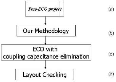
is-sue and coupling capacitance isis-sue together. In this thesis, we have developed the methodology to locally decrease injures of voltage drop and coupling capacitance in ECO stage with a few times consuming and routing resources. There are some works including data preparing, floor plan, placement, routing, static power anal-ysis and static noise analanal-ysis. A well-known deep submicron APR tool, Astro, is applied in our framework for voltage drop analysis and verification. To combine ECO algorithm considering CVE (coupling capacitance vilation elimination) with our methodology as shown in Figure 1.1. Not only the coupling capacitance but also voltage drop violations will be mitigated in our framework application.
Figure 1.1: A new ECO flow considering coupling capacitance and voltage drop. (a) general ECO (b) voltage drop decreasing in our methodologycoupling (c) capacitance violation elimination in ECO with CVE (d) layout checking after this new ECO flow
1.3
Thesis Organization
We will talk about preliminaries, methodology, experimental result, and conclusion in following chapters. We illustrate the definition and application for ECO in chapter 2. Some ECO-related papers were proposed in chapter 3. We illustrate the detail
methodology including compensating flow, power analysis, and noise analysis in chapter 4. Chapter 5 shows the experimental results. Finally, we give conclusions and future works in chapter 6.
Chapter 2
ECO (Engineering Change Order)
ECO is the process of inserting a logic/physical change directly into the netlist. ECO is beneficial because there is no need for full HDL synthesis. ECO is a subsequent step of APR flow. Furthermore, ECO can save lots times and money that is charged by ASIC vender. Traditionally it is regarded as very hard task to perform ECO that involves more than a few hundreds of gate. There are a few approaches for doing an ECO including:
• Manual fixing
• Regular synthesis tools with different placement tools
• Formal equivalence tools to do an ECO
We will first describe basic concepts about ECO, then some practical ECO flows.
2.1
ECO Basic Understandings
There are two main scenarios for doing an ECO
• Doing a spin to an existing design for fixing a bug or adding some features
In both cases we want to change a netlist with minimum effort and cost. An ECO is a local change and therefore there is not necessary to globally modify netlist. In many cases doing an ECO does not require new clocks, and it will reduce the time and effort required if comparing it to a full netlist spin.
Some of ECOs can be done as a metal fix only, which means new gates will be implemented with spare cells and only the wiring mask will be updated. This reduces the cost of the spin. Here we talk about ECO by limiting the synthesis tool to using spare cells only. When doing an ECO there is no need to rewire the full design, it is possible to only rub an incremental wiring job to do the local area of the ECO.
In many cases ECO will be much faster to update the netlist with an ECO flow than with a full synthesis of the design.
2.2
Traditional ECO Flows
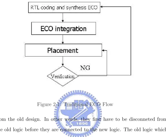
The traditional ECO flow is composed of four stages as shown in Figure 2.1.
(1) RTL coding and synthesis ECO –
The needed change in the design as it would be written in high level language. Limitations on how the new code needs to be written depends on the way that the ECO will be later synthesized. Then the new code should be synthesized for matching all synthesis constraints
(2) Integration of the ECO netlist into the design –
After synthesizing the new code we have two netlists, which have to be merged into a single netlist. This stage is usually done by a script that connects all of the ECO’s inputs to the proper drivers and all of the ECO’s outputs to the cells that they have to drive. The cells that are driven by the ECO are the cells
Figure 2.1: Traditional ECO Flow
from the old design. In other words, they first have to be disconneted from the old logic before they are connected to the new logic. The old logic which is now floating after it was replaced by the new logic can be either terminated or recursively cleaned by the script.
(3) Placement of the modified design –
Now that we have the ECO netlist integrated into the design, the new ECO cells need to be placed in legal placements between the existing cells of the old design.
(4) Design Verification –
The last stage is to check that the design is fully legalized and that there are no timing violations because of the connection stage and the placement stage. These checks usually fail on the first few iterations and there is a need to go back to one of the previous stage and fix the failures.
2.3
Freeze ECO Flow
Usually the revision of design is implemented by freeze ECO flow. There are some main steps in freeze ECO flow.
• New verilog in
• Expanding netlist
• Open library, copy a new cell from old one
• Selecting spare cells and grouping them
• Marking spare group for spare cells
• Opening new cell
• ECO compare, close cell
• Writing the compare result into file
• Opening the new cell again
• Freeze silicon
• ECO route
• DRC checking
• Stream out
2.4
ECO Flow using Physical Compiler
Some commercial tools have ECO, such as Astro[13][1], Physical Compiler[14], Laker[2],Mentor Graphic[18]. The ECO flow that uses Physical Compiler is com-posed of three stages[14].
• RTL coding of the ECO
• Synthesize the new ECO code using Physical Compiler
Chapter 3
Preliminaries
3.1
Previous Works on ECO
There are some discussions about ECO (engineering change order)[11][12][19][7][8][6] [10][9],or power supply planning [5][17][3][4], and power-signal codesign issues [15][16]. In this section, we describe some of the approaches in ECO, including on-chip bus ECO [7] and overlap removal ECO [11][19]
3.1.1
On-chip Bus ECO Optimization
It is clear that system-on-chip has usually high operating frequency of multi GHz [7] in current VSLI design. The interconnection becomes more critical in deep sub micron era because of sheet resistance increasing. However, on-chip bus architecture is more sensitive to noise as technology scales down. Various methods are proposed to solve the noise problem in on-chip bus architecture, among which bus shielding is used for noise avoidance for critical signals, and twisting wires is usually used to reduce the capacitance coupling noise more effectively in the complementary bus architecture. The graph is shown in Figure 3.1.
Some metal wires have been changed route due to ECO. It could become obsta-cles because of overlapping between updated wire segment and bus wire segments
Figure 3.1: On-chip Bus ECO Optimization [7].A complementary bus is composed of pair of wires, such as (B0P,B0N),(B1P,B1N) These ECO changes introduce obstacles that overlap with existing twist.
in the area of twisted bus structure. It is a challenge to remove the overlap without disturbing noise. It is necessary to find an excellent twisted bus architecture. [19] tries to solve this problem with MTBL (multiple twisted bit-line scheme). This TPG (twist pattern generation) can not only to minimize the number of twist while re-ducing the coupling capacitance not also to solve the overlap problem during ECO. This complexity of algorithm is O(V2 + E).
3.1.2
Removing Overlaps between Power and Signals
[19] proposes PSO (Power rail and Signal wire Overlap) problem which solves over-laps between power rails and signal wires due to the changes in power rail design on the top layer of a multiple layer routing region. It emphasizes that the new routing solution should satisfies the following constraints.
• Keep the routing of power rails in the new design unchanged
• Only the routing of top two layers is changed
• Horizontal (vertical) signal wire segment on the top layer can only move up/down (left/right)
In this paper, it proposes polynomial-time algorithms to solve the overlaps on the top layers as well as satisfying the allowable deviation bound, order consistency (there is no line inserted between two existing wires during ECO), track consis-tency, P-constraint and wire separation requirement, as shown in Figure 3.2. This paper propose two polynomial-time algorithms (PSO-G, PSO-H) to solve the over-laps between power rails and signal wires on the top layer as well as satisfying the deviation bound, order consistency, track consistency, P-constraint and wire sepa-ration requirement. PSO-G is a PSO algorithm with searching the graph in both direction. PSO-H is a faster PSO-G algorithm.
3.1.3
Removing Overlaps for Coupling Capacitance
Reduc-tion during ECO
[11] addresses not only in overlaps between power and signals issue but also in cou-pling capacitance reduction during ECO. It proposes that the situation about the overlap between signals increases coupling capacitance should be eliminated. A al-gorithm proposed two stage coupling capacitance violation elimination alal-gorithm. It can eliminate coupling capacitance for a given routing design as well as minimizing the total deviation. The first step(FCVE) processes signal wire segments to find a clean routing solution. The second step(SCVE) makes efforts to the minimize the total deviation based on the shortest path algorithm.
FCVE (First Stage Coupling-capacitance Violation Elimination)
FCVE processes signal segments from top to bottom on the layer L one by one and try to find a clean routing solution satisfying some constraints including :
Figure 3.2: Removing overlaps between power and signals [19]. The thick lines are power lines (P1,P2), the others are signal wires.M5 is presented by solid lines;dotted lines are for M4 (a)Some wire segments on M5 overlap with P1 and P2 during ECO. (b)A feasible PSO solution. (c)A solution with P-constraint(power-constraint), track consistency and order consistency violations.
• Only the routing of the top two layers is changed
• Obey P-constraint rule
• Deviation for each signal segment should not exceed the user-defined allowable deviation bound
SCVE (Second Stage Coupling-capacitance Violation Elimination)
This approach tries to minimize the total deviation based on the shortest path algo-rithm. It processes the wire segments from bottom to top after FCVE. SCVE tries to solve CVEP (special case of CVE) problem. Here is CVEP example shown in Figure 3.3 .
Figure 3.3: Removing overlaps for coupling capacitance reduction during ECO [11]. (a) A CVEP problem with 3 signal wire segments A1, A2, and A3 and 3 power rails. The allowable deviation of A1, A2, and A3 is 2, and their coupling capacitance upper bound is 0. A1 and A2 violate the coupling capacitance requirement. (b) FSP(first step graph for CVEP) graph. (c) SP(segment position) graph. ¯G of CVEP problem.
The three dashed ellipsed indicate the possible positions of the three wire segments A1, A2, and A3, respectively. (d) An optimal solotion to the CVEP problem
3.2
Problem Formulation
Our problem is formulated as follows. Given a routed design with planned power de-livery solution, after performing ECO, find the place in design for maximum voltage drop and noise amount, and search for a path for power line and noise compensation in lower metal layer for most effectiveness.
Chapter 4
Our Methodology for Voltage
Drop Repair and Coupling
Capacitance Reduction
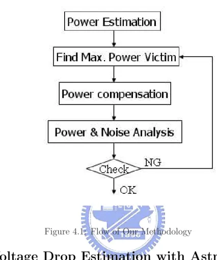
We develop a methodology to consider voltage drop and coupling capacitance during ECO. Our methodology is composed of six items as shown in Figure 4.1 .
• Voltage drop estimation with Astro
• Spot the severe IR drop region as power victim
• Do the compensating procedure
• Power analysis and noise analysis after compensation
• Go back step 2 if voltage drop checking is not good
We use only Astro (APR tool) to do the whole related experiments in our frame-work due to the database’s integrity.
• Do an APR job including floorplanning, placement, and routing
• Do static voltage drop analysis (IR drop analysis)
Figure 4.1: Flow of Our Methodology
4.1
Voltage Drop Estimation with Astro
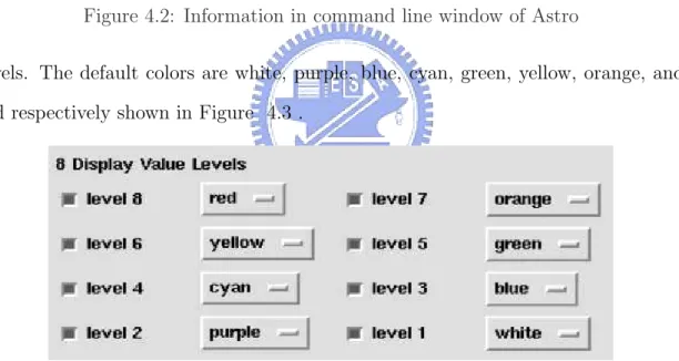
Before doing estimation, we have prepared a routed case for our experiment. The commercial APR tool, Astro[1], provides a friendly interface to estimate not only static and dynamic power information checking but also static noise analysis for customer,as shown in Figure 4.2 . At first, some specifications should be highlighted:
• All metal lines can rip-up and re-route in compensating path
• Do the floor-planning with Double Back (Vss-Vss)type
• Only one power net, Vdd or Vss, can be compensated in one chip
In the placement stage of APR, the standard cell should be placed as double back type, which means every-two rows share their own ground straps. Based on the power analysis of Astro, the levels of voltage drop will be displayed in eight
Figure 4.2: Information in command line window of Astro
levels. The default colors are white, purple, blue, cyan, green, yellow, orange, and red respectively shown in Figure 4.3 .
Figure 4.3: Power map shown with eight display value levels
4.2
Spot the Severe IR Drop Region
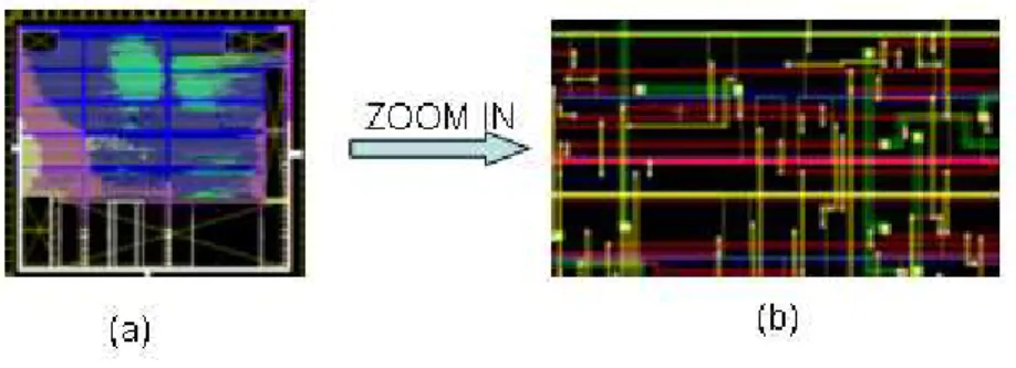
We found the location of maximum voltage drop region in previous stage. Then we can zoom into the local severe voltage drop region according to the coordination provided by command line window of Astro as shown in Figure 4.4 .When zooming in the local region. We can get many net attributions in neighboring area.
Figure 4.4: Whole-chip view zoom in to maximum voltage drop view (a)The map of whole chip after power analysis. (b)Spot the severe IR drop region
4.3
Voltage Drop Compensation
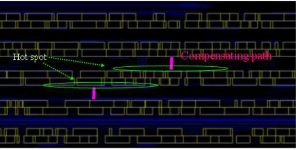
Here we introduce the concept of voltage drop compensation. In our methodology, we need to compensate the severe voltage drop region fro voltage drop repair. Based on the double-back floor-plan style, we view the neighboring power nets as candidates of power compensators. When we find the location of the power wire that suffer from the maximum voltage drop, the upper power wire or lower power wire will be as power compensator. Not only power victim but also power compensator are implemented with metal one layer for the effectiveness of repair. We could balance power victim and power compensator by adding additional power wires across them using metal one layer as shown in Figure 4.5 .
Figure 4.5: Concepts of Power Compensation. If the severe IR drop location (hot spot) found, the voltage supply compensator must be the upper power strap or lower power strap. We should route a metal-one power line connecting the severe IR-drop power line and compensator through compensating path
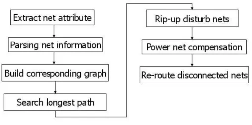
The procedure consists of a few stages as follows, shown in Figure 4.6:
(1) Graph-related data preparation
(2) Find the longest path for power compensation
(3) Rip-up disturb nets and route power net for compensation
Figure 4.6: Procedure of Power Compensation
4.3.1
Graph-related Data Preparation
There are three sub-stages in this stage, including net attribute extraction, net information parsing, and corresponding graph building.
• Extract net attribute –
We do the power analysis using Astro when the design after performing used ECO. Then we can get the power information from Astro. We can zoom in the design and obtain the maximum voltage drop region that displayed with metal one layer only.
• Paring net information –
There are many information in Astro log file with lots of dummy information for us. So we parse the file and get useful text file for the following stage.
• Build corresponding graph –
We can construct a directed graph with parsed text file as shown in Figure 4.7 .
Figure 4.7: Corresponding graph from text file. (a)A text file has been parsed from Astro. (b)The node is wire name, the directed edge is two neighboring horizontal wires. The weight of edge means the amount of coupling capacitance
4.3.2
Find the Longest Path for Power Compensation
First, we should illustrate the definitions about vertex, edge, and weight on edge in corresponding graph. A vertex is a horizontal wire segment in metal-one layer. A directed edge is two neighboring wires. The meaning of weight on edge is the amounts of coupling capacitance induced by two neighboring wires. We can generate paths base the previous definitions. There are many path among the graph as shown in Figure 4.8 . The path always from one root node to one leaf along the directed paths. The directed paths have a weight on the connecting two nodes. We can determine the longest path (the biggest coupling capacitance path) among all paths. If we choose the longest path as the compensating path of voltage drop, we can solve both voltage drop and coupling capacitance together. It is what we say that we find the location of coupling capacitance with this algorithm. And the longest path is the compensating path of our methodology as shown in Figure 4.9 .
Figure 4.8: Path property – A circle is a vertex (a wire) and a directed edge means two neighboring wires. A weight on edge is the amount of coupling capacitance.
Figure 4.9: Path generation of corresponding graph – There are five paths from root to leaf. The longest path among all paths is the path contains the biggest coupling capacitance
4.3.3
Rip Up the Disturb Nets and Route Power Net for
Compensation
There are must many signal wire segments on the longest path from previous step. We should cut off these nets according to the result of previous stage as shown in Figure 4.10 .
Figure 4.10: Rip up these dirturb nets viewed as obstacles for power compensating path.
Due to these disturb nets removal, so we can draw the metal one wire segment across the power victim and power compensator as shown in Figure 4.11 .
4.3.4
Re-route these Disconnected Nets
These disconnected signal wire should be re-routed for functional consistency as shown in Figure 4.12 .
Figure 4.11: Power net compensation when these disturb net ripped already.
4.4
Power Analysis and Noise Analysis after
Com-pensation
When the compensation procedure is done, we should analyze the performance about static voltage drop and static noise.
If the requirement is not met, we will go back to find another path and perform voltage drop compensation, until the requirement is met.
Chapter 5
Experimental Results
Our algorithms were implemented in C++ on 3GHzPC (memory 1GB) to do the following jobs:
• Parsing the net-attribute file
• Find the longest path in corresponding graph
The remainder of our methodology were integrated with Astro, including APR, power, and noise analysis.
We do two experiments about small size design and medium size design with TSMC 0.13um node (four metal layers). The specifications are presented in Table 5.1 .
Design # of Macros # of STD Cells Total wire lengths Function
small size 2 1100 152765 decoder
medium size 13 20286 1658612 controller
5.1
Power Analysis and Noise Analysis in Astro
We will introduce the power and noise analysis tools in Astro and try to present how those functions work.
5.1.1
Power Analysis
The power engine of Astro is Astro-Rail. It is to resolve power, voltage drop and electromigration problems that can occur during physical design process. After global routing, use Astro-Rail to detect potential violation and fix before detail route. When detail route or ECO is complete, we can use Astro-Rail to verify the design for sign-off analysis.
The procedure of static power analysis is as follows:
• Purging existing PG(power/ground) extraction
• PG extraction
• Load power supply
• Load net switching activity
• Power analysis
• P/G Rail analysis
• Power map display
5.1.2
Noise Analysis
Astro-Xtalk can prevent, analyze, and fixe crosstalk violations to ensure signal in-tegrity. It performs crosstalk-induced noise and delay analysis to identify any re-maining violations. The procedure of static noise analysis is as follows:
• Generating a PARA(parasitic) view – to get some distributed coupling capac-itance information
• Setting timing setup options – to set crosstalk-related options in this environ-ment
• Specifying power supply – noise metrics are percentages of the power supply voltage
• Input from CLF and noise library – Astro-Xtalk can use noise constraints from a CLF(cell library format) file and noise response information from noise library
• Crosstalk analysis
5.2
Voltage Drop Results
In the small-size design, it has a little voltage drop compared with medium-size design in same power strap style. It is obvious that medium-size design has great improvement of voltage drop during power compensation.These result is shown in Table 5.2 .
Design Status Max. IR Drop(mV) small size pre-compensating 74
small size post-compensating 67 medium size pre-compensating 245 medium size post-compensating 199
Table 5.2: Power Analysis with small/medium size design during voltage drop com-pensation
5.3
Coupling Capacitance Result
Here we focus the static noise experiments and detect crosstalk amount of signals in severe voltage drop region. We do two static noise experiments with medium-size design. One experiment is implemented with re-routing the disconnected nets automatically(with Astro’s functon). The other one is implemented with re-routing the disconnected nets by hand. They have difference about coupling capacitance reducing.The result is shown in Table 5.3 .
Status X’tal(R,F) (Vdd) –auto X’tal(R,F)(Vdd) –manual pre-compensating 0.033, 0.029 0.033, 0.029
post-compensating 0.028, 0.024 0.019, 0.018
Table 5.3: Static Noise Analysis during voltage drop compensation R: The calcula-tion for rise considers the victim at steady-state low and the aggressors switching from low to high. F: The calculation for fall considers the victim at steady-state high and the aggressors switching from high to low.
5.4
Voltage Drop and Crosstalk Results with
Dif-ferent Voltage
There are some improvements about voltage drop and coupling capacitance with medium-size design.It is obvious that they have no change with different voltage.The result in shown in table 5.4 . The unit of Vdd is volt, and the unit of Max. IR drop is milli-volt.
Vdd Status Max. IR drop X’tal(R,F) –auto X’tal(R,F)–manual 1.8 pre-compensating 245 ( 0.033,0.029 ) ( 0.033,0.029 ) 1.8 post-compensating 199 ( 0.028,0.024 ) ( 0.019,0.018 ) 1.2 pre-compensating 163 ( 0.033,0.029 ) ( 0.033,0.029 ) 1.2 post-compensating 132 ( 0.028,0.024 ) ( 0.019,0.018 )
Table 5.4: Power analysis and crosstalk analysis with different voltage
Finally we try to do some comparisons during ECO with different power value. It is obvious that they have no change with different voltage. Our methodology can not change power consumption.
Vdd IR Drop improved X’tal improved –auto X’tal improved –manual power (mW)
1.8 18.7% 16 % 40 % 698
1.2 19 % 16 % 40 % 310
Table 5.5: Performance comparison with different voltage
We show some figures about power analysis and crosstalk analysis. First, about the small-size design, two different power compensating styles are shown in Figure 5.1 . Another power compensating styles are shown in Figure 5.2 . The compen-sating performance of the four types are 5%, 9%, 10%, and 5% respectively with total voltage drop improvement. Second, about the medium-size design, the power compensating sample is shown in Figure 5.3 .This example has 19% voltage drop improvement. Finally, we want to discuss about how these disconnecting nets re-route work. The original graph is shown in Figure 5.4 and two routing types are shown in Figure 5.5 .
Figure 5.1: (A) Route power net across Ground strap (B) Route three-bar power net (type I)
Figure 5.2: (A) Route three-bar power net (type II) (B)Route three-bar power net (type III)
Figure 5.3: Route power net in medium-size design
Figure 5.5: (A)Manual route after compensating (B)Auto route after compensating Manual route is to route these disconnecting wires with hand. Auto route is to route these disconnecting wires by Astro’ command
Chapter 6
Conclusions and Future Works
In this thesis, we proposed an effective methodology to repair voltage drop and reduce local coupling capacitance. The methodology that follows with coupling ca-pacitance elimination algorithm [11] might be a solution to solve voltage drop and coupling capacitance issue in ECO stage of later physical design. This methodology indeed improve a lot for power and noise disturb. It could be a good candidate to solving these problems when integrated with commercial APR tool.
However its algorithm should be verified with different designs. It could be a chal-lenge to get a nice signal integrity for clock signal when we rip up clock wire segment in compensating procedure. It will be better for this methodology to be merged into APR tool with these own database access protocol,such as Milkyway database access through Astro’s API interface. The methodology considering dynamic noise anal-ysis should be handled and analyzing the whole metal layers coupling capacitance instead of metal one layer only in the future.
Bibliography
[1] “Astro User Guide”.
[2] “Laker PnR editor”. 2005.
[3] G Bai, S Bobba, Hajj, and I.N. “Power bus maximum voltage drop in dgital VLSI circuits”. pages 263–268, Mar. 2000.
[4] Hung-Ming Chen, Li-Da Huang I-Min Liu, and M.D.F Wong. “Simultaneous power supply planning and noise avoidance in floorplan design”. IEEE Transactions on Computer-Aided
Design of Integrated Circuits and Systems, 24:578–587, Apr. 2005.
[5] Jun Cheng Chi, Tsung Hui Huang, and Mely Chen Chi. “An IR drop-driven placer for standard cells in a SOC design”. volume 2, pages 29–32, Sept. 2005.
[6] J Cong, Jie Fang, and Kei-Yong Khoo. “An implicit connection graph maze routing algorithm for ECO routing”. Proceedings IEEE/ACM International Conference on Computer-Aided
Design, pages 163–167, Nov. 1999.
[7] L Deng, Wong, and M.D.F. “Optimal algorithm for minimizing the number of twists in an on-chip bus”. volume 2, pages 1104–1109, Feb. 2004.
[8] Xiaopeng Dong, inhwan Seo, and W Kao. “New metal fill considerations for nanometer technologies”. volume 2, pages 802–805, Oct. 2005.
[9] Wang Donghui, Yu Qian, Hong Ying, and Hou Chaohuan. “SuperV back-end design flow based on Astro”. Proceedings of the IEEE, 2:1524–1527, Oct. 2005.
[10] Xiang Hua, Li-Da Huang, Kai-Yuan, and M.D.F Wong. “An ECO algorithm for resloving OPC and coupling capacitance violations”. Proceedings of the IEEE, 2:873–876, Oct. 2005.
[11] Xiang Hua and C. Kai-Yuan. “An ECO Routing Algorithm for Eliminating Coupling Capac-itance violations”. IEEE Transactions on Computer-Aided Design of Integrated Circuits and
Systems, 2005.
[12] Xiang Hua, C. Kai-Yuan, and M.D.F Wong. “An ECO Algorithm for Eliminating Crosstalk Violations”. Proceedings International Symposium on Physical Design, PP:41–46, Apr. 2004.
[13] Niv Margalit. “Astro Hierarchy Preservation and Hierarchical Verilog Ouput Applicaton Note”. Aug. 2003.
[14] Niv Margalit. “ECO Flow - Using Physical Compiler”. volume 1, 2004.
[15] J Singh and S.S Sapatnekar. “Congestion-aware topology optimization of structure power/ground networks”. IEEE Transactions on Computer-Aided Design of Integrated
Cir-cuits and Systems, 24:683–695, May 2005.
[16] Jaihua Su, Jiang Hu, S.S Sapatnekar, and S.R Nassif. “Congestion-driven codesign of power and signal networks”. Proceedings IEEE/ACM Design Automation Conference, pages 64–69, June 2002.
[17] Xiaohai Wu, Changge Qiao, and Xianlong Hong. “Design and optimization of power/ground network for cell-based VLSIs with macro cells”. volume 1, pages 21–24, Jan. 1999.
[18] www.mentor.com/cicd. “IC Station Tool Suite”. 2005.
[19] Hua Xiang, C. Kai-Yuan, and Wong D.F. “ECO algorithms for removing overlaps between power rails and signal wires”. Proceedings IEEE/ACM International Conference on
![Figure 3.1: On-chip Bus ECO Optimization [7].A complementary bus is composed of pair of wires, such as (B0P,B0N),(B1P,B1N) These ECO changes introduce obstacles that overlap with existing twist.](https://thumb-ap.123doks.com/thumbv2/9libinfo/8582691.189424/21.918.212.695.154.342/figure-optimization-complementary-composed-introduce-obstacles-overlap-existing.webp)
![Figure 3.2: Removing overlaps between power and signals [19]. The thick lines are power lines (P1,P2), the others are signal wires.M5 is presented by solid lines;dotted lines are for M4 (a)Some wire segments on M5 overlap with P1 and P2 during ECO.](https://thumb-ap.123doks.com/thumbv2/9libinfo/8582691.189424/23.918.204.668.239.901/figure-removing-overlaps-signals-presented-dotted-segments-overlap.webp)
![Figure 3.3: Removing overlaps for coupling capacitance reduction during ECO [11].](https://thumb-ap.123doks.com/thumbv2/9libinfo/8582691.189424/24.918.233.677.519.899/figure-removing-overlaps-coupling-capacitance-reduction-eco.webp)