High Temperature Operated (-250 K) Photovoltaic-Photoconductive (PV-PC)
Mixed-mode
InAs/GaAs
Quantum Dot Infrared Photodetector
Shiang-Feng Tang, Shih-Yen Lin, Si-Chen Lee, and Chieh Hsiung Kuan
Department of Electrical Engineering, National Taiwan University, Taipei, Taiwan, R. 0. C..
Ya-Tung Cherng
Materials & Electro-Optics Division, Chung Shang Institute of Science and Technology, Lung Tan, Taiwan, R. 0. C..
Abstract
The 10 stacked self-assembled InAdGaAs quantum dot infrared photodetector (QDIP) operated in 2.5 to 7 pm range by photovoltaic (PV) and photoconductive (PC) mixed-mode near room temperature (-250 K) was demonstrated. The specific peak detectivity D* is 2.4 x 10’ cm-Hz’”/W at 250 K. The confining AlxGal.xAs barrier layers on both sides of stacked QD structure -are key to the high temperature operation
Introduction
In the past several years, AlGaAs/GaAs quantum well infrared photodetector (QWIP) had been widely investigated due to its commercial and military applications [l-21. A similar Structure, InAs/GaAs quantum dot infrared photodetector (QDIP) was proposed and investigated in several reports both in theoq and in practical devices [3-71. The most dramatic effect of using QDIP instead of QWIP to detect mid- and far- infrared signal is its h g h temperature performance [7]. For QWIP, devices can rarely be operated beyond 100 K. However, QDIP operated over 100 K had been presented in several reports [6-71. In this letter, the characteristics of self-assembled InAs QDIP with high temperature operation is presented.
AulGelNi 1 0 x 1 50 mi Al,,Ga,,As undoped 3 ML InAs QDs +n=1
x
1018ciii~ 30 mi GaAs undoped 50 nni A l , , G a , , A s undoped 1 piGaAs n=l X 10 18cm-’I
450 p i n Senu-Insulating (001) GaAsI
Fig. 1 Schematic diagram showing the device structure of InAdGaAs QDIP.
Experiments and Discussion
The self-assembled I d s quantum dots discussed in this letter were grown on (100) GaAs semi-insulating substrate in Stranski-Krastanow (S-K) growth mode using solid-source MBE under As deficient condition. The substrate temperature was kept at 510 “C during MBE growth. The detector structure consists of 10 stacks of 3 ML InAs quantum dot layers seperated by 30 nm GaAs barrier. The self assembled InAs dot was uniformly doped to 1 X 10l8 ~ n i - ~ with undoped GaAs barrier. The dot density is approximately 4 ~ 1 0 ’ ~ cni-’. Two extra Alo 3Gao ,AS confining layers were grown on both sides of the 10-stacked QD structure to reduce dark current and preserve photoexcited carriers. 0.5 pm and 1 pm GaAs
with doping density 1 X 10” cm-3 were grown to provide top
24.4.1
1 - . 1
-0.5 0.0 0.5 1.0
Voltage (V)
Fig. 2 Dark I-V characteristics of the QDIP from 10 to 300 K. The dotted curve represents the photocurrent measured at 10 K when the QDlP is illuminated from the ambient background radiation through the cryostat window at 10 K.
and bottom contacts, the schematic device structure is shown in Fig. 1.
Using standard procedure, contact metal evaporation, photolithography and wet etching, l O O X 100 pm2 devices are fabricated. The current-voltage (I-V) characteristics of the device were measured by HP4 156b semiconductor parameter analyzer. And the spectral response was measured under edge-coupling scheme with APD cryogenics and a Perkin-Elmer S2000 FTIR spectroscope, which is a standard configuration for QWIP measurement [SI. To obtain the absolute value of responsivity, calibration
was
made by using a black body source and a chopper to chop the infrared signal such that the corresponding photocurrent can be detected by SR830 lock-in amplifier.Figure 2 displays the dark I-V characteristics of the device. The photocurrent measured at 10 K while QDIP was illuminated from the ambient background radiation is also shown as dotted curve which appears to be larger than the dark current at 250 K under the bias of ? 1 V indicating the background-limited-performance temperature (BLIP) to be 250 K. Figs. 3 (a) and (b) show the temperature-dependent photoresponsivity and peak specific detectivity of QDIP at zero bias which gives a direct evidence that this device can be operated at 250 K in photovoltaic (PV) mode. And from Fig. 3 (b), it is shown that the peak specific detectivity is 2.4 x
0.1
-
50 100 150 200 2%
Temperature (K) (b)
\I
Fig. 3 (a) The responsivity of QDlP as a function of temperature at zero bias. (b) The specific detectivity of QDlP as a function of temperature at zero bias.
lo8 cm-Hz"*/W at 250 K. To our knowledge, this is the highest value for QDIP operated at a temperature beyond 200 K in the 2.5 to 7 pm wavelength range.
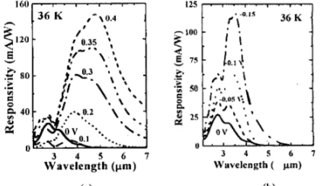
Figures 4 (a) and (b) show the responsivity of QDIP operated at 36 K, the peak responsivity of 25 mA/W at the range of 2.5
-
4 pm was observed at zero bias which decreased to almost zero at positive 0.1 V but increased at negative biases. That is clearly a PV mode operation. However, in the wavelength range from 3.5 to 7 pm, the peak responsivity is dependent on the biases which vanishes atzero bias, this is a photoconducitivity (PC) mode operation. The peak responsivity at +0.42 V is 155 mA/W at a wavelength of 5 pm. The asymmetric photoresponse is attributed to the segregation of doped Si atoms toward the top surface of the QD and results in asymmetric electric field
I A Z h l 3 4 5 6 7
Waveiengih ( i m ) ' Wavelength ( pm)
(a) (b)
Fig. 4 The responsivity of QDlP at (a) positive bias from 0 to 0.4 V, (b) negative bias from 0 to - 0.15 V. The temperature i s 36 K.
24.4.2
voltage. Thus the PV mode response is formed.
A simple model is proposed to explain the mechanism
0.15 0.1 resulting in high-temperature operation by QDIP. By
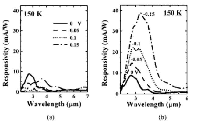
measuring the recovery of resist after the device is shielded from the glowbar, the recovery time constant is found to be extremely long, i.e., 6.64 sec, which suggests that the photoexcited electrons are difficult to be recaptured by QDs (a) (b) unless under rather high temperature. This is the negative bias from 0 to - 0.15 V. The temperature is I50 K. high-photoelectric-gain nature of QDIP. [3] And the AIo &3ao ,AS blocking layers prevent the photoelectrons to escape from the QD structure and thus photoelectrons are accumulated inbetween. Hence, the electron quasi Fermi level is raised very high as compared to that under dark environment. The photocurrent is much enhanced which explain the high temperature operation of the device.
.-
v13 4 5 6
3 4 5 6 1
Wavelength (pm) Wavelength (pm)
Fig. 5 The responsivity of QDIP at (a) positive bias from 0 to O.lSV, (b)
distribution which lead to charge separation. Figs. 5 (a) and (b) display the photoresponsivity of QDIP at 150 K, which is dominated by PV mode. The PC mode almost disappears due to the large dark current with increasing bias. The PC mode and PV mode response of the device are attributed to two different mechanisms. The 3.5-7 pm response (PC mode) are due to ground state Eo to bound excited state E, transition in
the quantum dots as shown in Fig. 6. The photoexcited electrons would tunnel through the sharper barrier formed due to the segregation of Si dopant along the growth direction at positive bias. The 2.5
-
4 pm responses are due to electron bound state Eo to continuum states E2 transition, once electrons jump out of the volcanic shaped potential, they are driven by the internal asymmetric electrical field in GaAs toward the substrate side and form a positive open circuitConclusion
In conclusion, with the combination of QD and two blocking barrier, the operation temperature of our QDIP is pushed up to 250 K. With PC and PV mode response coexistence, the peak specific detectivity D* is 2.4 x 10’
cm-Hz’’*/W at 250 K, which is, to our knowledge, the highest value for QDIP operated at a temperature beyond 200 K in the 2.5 to 7 p m range.
Barrier
+
References
lowerring
Growth Direction
diffusion
due to
Si
( 1 ) S D Gunapala, S V Baiidara, J K Liu, W Hong, M Sundarain, P D Maker, R E Muller, C A Shott, and R Carralejo, IEEE Trans Electron Devices 45, 1890 ( 1 998)(2) C J Chen, K K Choi, W H Chang, and D C Tsui, Appl Phys Lett
72, 7 (1 998)
V Ryzhii, Semicond Sci Techno1 11. 759 (1996)
S Xu, S J Chua, T Mei, X C Wang, X H Zhaiig, G Karunasiri, W J
Fan, C H Wang, 1 Jiang, S Waiig, aiid X G Xie, Appl Phys Lett 73, 3153 (1998)
(3) (4)
GaAs
InAsGaAs
Fig 6 The schematic band diagram of the InAs QD surrounded by in GaAs barrier along growth direction, where EO, El represent the first and second confined ststes and E2 i s the quasi continuum state
24.4.3
(5)
(6) S . Kim, H. Mohseni, M. Erdtmann, E. Michel, C. Jelen, and M. D. Pan and E. Towe, Appl. Phys. Lett. 75,2719 (1999).
Razeghi, Appl. Phys. Lett. 73,963 (1998).
(7) J . W. Kim, J. E. Oh, S . C. Hong, C. H. Park, and T. K . Yoo, IEEE Trans. Electron Devices Letters 21, 329 (2000).
I<. K . Choi, '' The Physics of Quantum Well Infrared Photodetectors ", World Scientific Publishing, Singapore, Chap. 6 (1997).
(8)