1740 IEEE ELECTRON DEVICE LETTERS, VOL. 32, NO. 12, DECEMBER 2011
Photoerasable Organic Nonvolatile Memory Devices
Based on Hafnium Silicate Insulators
Fang-Chung Chen and Hsiao-Fen Chang
Abstract—We have prepared photoerasable organic nonvolatile memories using high-dielectric (high-k) hafnium silicate as device insulators. The high-k material can effectively lower the operating voltage of the organic memory devices. The nonvolatile memory can be written by applying a gate bias and be effectively erased by photon illumination. The spectral study of the photoinduced recovery effect indicated that the erasing mechanism should be relevant to the recombination between the trapped charges and the photogenerated exctions.
Index Terms—Absorption, high-k gate dielectrics, nonvolatile memory, organic semiconductors.
I. INTRODUCTION
O
RGANIC memory devices are receiving increasing atten-tion because of their favorable properties, such as low cost, light weight, flexibility, and fabrication at low tempera-ture, which can help to save the energy [1]–[5]. While many types of organic memory devices have been demonstrated, organic nonvolatile memories (ONVMs) are of particular in-terest because the data can be retained, even when the supply power has been turned off [1]–[3]. Many approaches, such as organic bistable devices [1]–[3], organic field-effect tran-sistors (OFETs) based on ferroelectric gate insulators [4], [5] have been proposed for the fabrication of ONVMs. In 2006, Baeg et al. demonstrated ONVMs with polymeric chargeable dielectrics, which can also be called electrets; the OFET mem-ories used a simple device configuration and showed high performance [6]. However, the voltage required to operate the device was somehow large, and the operating mechanism is still not fully understood yet.The use of high-dielectric (high-k) materials can afford higher surface charge densities at the semiconductor/dielectric interface. As a result, devices with higher current and/or lower operating voltage could be obtained [7], [8]. In this work, an organic memory device with a high mobility and a low operating voltage will be demonstrated by using hafnium (Hf) silicate as the gate dielectric layer (k = 7.14). Furthermore,
Manuscript received August 8, 2011; revised August 31, 2011; accepted September 7, 2011. Date of publication October 19, 2011; date of current version November 23, 2011. This work was supported in part by the National Science Council and in part by the Ministry of Education through the ATU plan. The review of this letter was arranged by Editor T. Wang.
F.-C. Chen is with the Department of Photonics and Display Insti-tute, National Chiao Tung University, Hsinchu 30010, Taiwan (e-mail: [email protected]).
H.-F. Chang is with the Institute of Electro-optical Engineering, National Chiao Tung University, Hsinchu 30010, Taiwan.
Color versions of one or more of the figures in this paper are available online at http://ieeexplore.ieee.org.
Digital Object Identifier 10.1109/LED.2011.2168375
the device could be electrically written and read and be erased through photon irradiation. The mechanism of the photoin-duced recovery has also been investigated. The ONVMs re-ported herein could be used as write-once–read-many-times (WORM) memories [9] with an additional photoerasable func-tion. The optically erasable feature might also help to simplify the external-circuit architecture [10].
II. EXPERIMENT
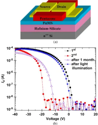
Fig. 1(a) displays a schematic representation of the device structure. Heavily n-doped Si wafers were used as substrates. A 90-nm-thick Hf silicate deposited by metal–organic chem-ical vapor deposition was served as the gate dielectric [11]. Tetrakis(diethylamido) hafnium (TDEAH) was used as the Hf precursor. A 0.1-M TDEAH solution in octane was vaporized at 140◦C and then injected into the chamber. The dielectric sur-face was further modified with a layer of poly-α-methylstyrene (PαMs) [6], [8]. The polymer was spin-coated from a 0.5 wt% solution in toluene. The sample was then postannealed at 100◦C for 1 h. The thickness of PαMs was∼30 nm. Next, a semiconducting layer of pentacene (60 nm) was thermally deposited on the dielectric layers. To complete the devices, gold was thermally deposited through a patterned shadow mask to serve as source and drain electrodes. The channel length (L) and width (W ) were 100 and 2000 μm, respectively. The electrical characteristics of the devices were measured by using a Keithley 4200 semiconductor parameter analyzer in the dark. To probe the photoresponse of the devices, an Oriel Hg lamp was used as a light source; a monochromator was also used to select the preferred spectral line during the measurements. The absorption spectra were obtained using a Perkin Elmer Lambda 650 spectrometer.
III. RESULTS ANDDISCUSSION
Fig. 1(b) shows the transfer curves of the organic memory device. In the first scan, the device exhibited typical p-channel field-effect behavior [8]. The hole mobility, which was cal-culated from the slope of the plot of the square root of the drain current (Id) versus the gate voltage (Vg) in the saturation
region, was 0.3 cm2V−1s−1. Meanwhile, the threshold voltage (Vth) and on-off ratio were−4 V and ∼ 105, respectively. In the second scan, however, the transfer curve was shifted toward the negative direction with a larger shift of Vth of ∼16 V. In the following scans, the curve stayed almost unchanged as the one of the second scan. We inferred that charges were probably trapped and stored in the PαMS layer [6] and/or in the deep
CHEN AND CHANG: PHOTOERASABLE ONVM DEVICE BASED ON HAFNIUM SILICATE INSULATOR 1741
Fig. 1. (a) Device structure fabricated in this study. (b) Transfer characteristics of the memory device measured under different conditions. Vdwas kept at −10 V. At the first scan, the device exhibited typical OFET characteristics.
At the second scan, we can clearly observe a large shift in the curve toward the negative direction. The memory effect still remained after one month. Further, the device almost recovered after white light illumination.
energy levels of the high-k material. The results suggested that the device described herein is suitable for the application of memory devices.
The number of trapped charges Δn can be determined from the following equation:
Δn = ΔVth
e Ci (1)
where e, ΔVth, and Ci are the element charge, the shift of
Vth, and the capacitance of the gate dielectric, respectively [12]. Using the equation, Δn was calculated to be 1.26× 1012cm−2. This number is similar to those reported earlier in the literature [6]. On the other hand, due to the higher capacitance of the dielectric layer we used, the operating voltage of our devices becomes lower. In short, the results here indicate that the use of high-k dielectric is a promising approach for decreasing the operating voltage of the ONVMs.
To release the trapped charges, we tried to apply positive gate biases on the device. However, no apparent Vth recovery was observed, even when a gate bias up to +50 V was applied (Fig. 2). While we further applied an even higher voltage, the dielectric layer started to breakdown, and a large leakage current was obtained. One possible reason the device cannot be electrically erased is that the charge carriers were trapped in the deep energy levels of the dielectric layers.
To erase the memory, the device was illuminated with a white light source (5.5 mW cm−1) for 6 min. We can see that the transfer curve almost recovered to its original position (Fig. 1),
Fig. 2. Relationship between the shift of Vth and the applied Vg under
different stress conditions.
suggesting that photons can be utilized to erase the memory. Previously, Baeg et al. have proposed a mechanism for memory devices fabricated with a similar device structure as that of our devices [Fig. 3(a)] [6]. They used SiO2 as the dielectric material. The authors suggested that the charges, which are field generated near the semiconductor/dielectric interface, might be deeply transferred and trapped in the PαMS layer, inducing the memory effect [6], [12]. Furthermore, a critical energy barrier exists between the pentacene and PαMS; illumination of photons can effectively lower the barrier and results in photoinduced relaxation of the trapped charges. In order to investigate the erasing mechanism of the memory reported herein, we simultaneously applied various positive gate biases and further illuminated the device. As shown in Fig. 2, we can see that Vth started to recover after we positively biased the device only for 10 s. If the stress time was further increased to 60 s, the device could almost recover to its original state, whereas Vg was only +10 V. The results in Fig. 2 clearly
revealed that photoillumination indeed can lower the energy barrier between the pentacene and PαMS layers.
To further understand the mechanism of light-induced recov-ery of the memory effect, we investigated the recovrecov-ery of the channel conductivity by illuminating the organic memory at different wavelengths. The fixed photon flux (Φ) at a certain wavelength (λ) was defined as
Φ = P
hν (2)
where h, P , and ν are Planck’s constant, the power inten-sity per unit second, and light frequency, respectively [12]. Photons with wavelength ranging from 450 to 670 nm were incident on the channel, whereas the flux was fixed at 1× 10¹⁴photons cm−2s−1. After illumination, the I–V curve was measured at a Vd bias of−10 V. From the shift of Vth, the number of the released charges could be calculated, following (1) [13]. As shown in Fig. 3, the released charge was found to be directly proportional to the absorption of pentacene. This result revealed that the photoinduced recovery was related to the pho-togenerated species in the pentacene thin film. We suspect that the photoexcited excitons directly recombined with the trapped charges in the dielectric layers and/or at the pentacene/dielectric
1742 IEEE ELECTRON DEVICE LETTERS, VOL. 32, NO. 12, DECEMBER 2011
Fig. 3. (a) Energy diagram and the proposed model for charge transfer and trapping between the dielectric layers and pentacene. The arrow indicates the possible charge transfer process between the pentacene and the dielectric layers. (b) Dependence of the number of released charges on the incident wavelength, as well as the absorption spectrum of the pentacene thin film.
interface. The results in Fig. 3(b) strongly indicate that the recovery mechanism should be relevant to the recombination between the trapped charges and the photogenerated exctions.
IV. CONCLUSION
We have shown that the use of high-k insulators can ef-fectively lower the operating voltage of ONVMs. The device can be written by applying a gate bias and be erased by light illumination. More importantly, through the investigation of
spectral response during the photoinduced recovery process, we have observed that larger absorption ability at the particular wavelength (in the red region) of pentacene led to a fast recovery rate. In summary, the results in this study can pave the way for the applications of low-power-consumption, flexible, lightweight, low-cost, and rewritable organic memory devices.
REFERENCES
[1] J. Ouyang, C. W. Chu, R. J. Tseng, A. Prakash, and Y. Yang, “Organic memory device fabricated through solution processing,” Proc. IEEE, vol. 93, no. 7, pp. 1287–1296, Jul. 2005.
[2] H. T. Lin, Z. Pei, J. R. Chen, G. W. Huang, J. F. Fan, and Y. J. Chan, “A new nonvolatile bistable polymer-nanoparticle memory device,” IEEE
Electron Device Lett., vol. 28, no. 11, pp. 951–953, Nov. 2007.
[3] B. Cho, T. W. Kim, S. Song, Y. Ji, M. Jo, H. Hwang, G. Y. Jung, and T. Lee, “Rewritable switching of one diode-one resistor nonvolatile or-ganic memory devices,” Adv. Mater., vol. 22, no. 11, pp. 1228–1232, Mar. 2010.
[4] B. Stadlober, M. Zirkl, M. Beutl, G. Leising, S. Bauer-Gogonea, and S. Bauer, “High-mobility pentacene organic field-effect transistors with a high-dielectric-constant fluorinated polymer film gate dielectric,” Appl.
Phys. Lett., vol. 86, no. 24, p. 242 902, Jun. 2005.
[5] K. Asadi, D. M. de Leeuw, B. de Boer, and P. W. M. Blom, “Organic non-volatile memories from ferroelectric phase-separated blends,” Nature
Mater., vol. 7, no. 7, pp. 547–550, Jul. 2008.
[6] K. J. Baeg, Y. Y. Noh, J. Ghim, S. J. Kang, H. Lee, and D. Y. Kim, “Organic non-volatile memory based on pentacene field-effect transistors using a polymeric gate electret,” Adv. Mater., vol. 18, no. 23, pp. 3179– 3183, Dec. 2006.
[7] C. D. Dimitrakopoulos, S. Purushothaman, J. Kymissis, A. Callegari, and J. M. Shaw, “Recent progress in polymer solar cells: Manipulation of polymer:fullerene morphology and the formation of efficient inverted polymer solar cells,” Science, vol. 283, pp. 822–824, Feb. 1999. [8] F. C. Chen, C. S. Chung, Y. S. Lin, L. J. Kung, T. H. Chen, and
H. P. D. Shieh, “Low-voltage organic thin-film transistors with polymeric nanocomposite dielectrics,” Org. Electron., vol. 7, no. 5, pp. 435–439, Oct. 2006.
[9] S. Möller, C. Perlov, W. Jackson, C. Taussig, and S. R. Forrest, “A polymer/semiconductor write-once read-many-times memory,” Nature, vol. 426, pp. 166–169, Nov. 2003.
[10] H. T. Lin, Z. Pei, J. R. Chen, and Y. J. Chan, “UV-erasable stacked diode-switch organic nonvolatile bistable memory on plastic substrates,” IEEE Electron Device Lett., vol. 30, no. 1, pp. 18–20, Jan. 2009.
[11] J.-H. Chen, D. Landheer, X. Wu, A. C. Jones, S. A. Rushworth, T.-F. Lei, and T.-S. Chao, “Evaluation of HfxSi1−xO2 deposited by
pulse-mode MOCVD using Hf(NEt2)4, ButMe2SiOH, and O2,” in Proc.
Int. Electron Devices Mater. Symp., Hsinchu, Taiwan, 2004, pp. 459–462.
[12] V. Podzorov and M. E. Gershenson, “Photoinduced charge transfer across the interface between organic molecular crystals and polymers,” Phys.
Rev. Lett., vol. 95, no. 1, p. 016602, Jul. 2005.
[13] A. Salleo and R. A. Street, “Light-induced bias stress reversal in polyflu-orene thin-film transistors,” J. Appl. Phys., vol. 94, no. 1, pp. 471–479, Jul. 2003.