Low-temperature growth of ZnO nanorods in anodic aluminum oxide on Si substrate by
atomic layer deposition
Ching-Jung Yang, Shun-Min Wang, Shih-Wei Liang, Yung-Huang Chang, Chih Chen, and Jia-Min Shieh
Citation: Applied Physics Letters 90, 033104 (2007); doi: 10.1063/1.2431786
View online: http://dx.doi.org/10.1063/1.2431786
View Table of Contents: http://scitation.aip.org/content/aip/journal/apl/90/3?ver=pdfcov Published by the AIP Publishing
Articles you may be interested in
Tuning of undoped ZnO thin film via plasma enhanced atomic layer deposition and its application for an inverted polymer solar cell
AIP Advances 3, 102114 (2013); 10.1063/1.4825230
Growth, optical, and electrical properties of nonpolar m -plane ZnO on p -Si substrates with Al2O3 buffer layers Appl. Phys. Lett. 100, 011901 (2012); 10.1063/1.3673346
Effect of temperature and gas velocity on growth per cycle during Al2O3 and ZnO atomic layer deposition at atmospheric pressure
J. Vac. Sci. Technol. A 30, 01A155 (2012); 10.1116/1.3670961
Core-shell nanowire arrays of metal oxides fabricated by atomic layer deposition J. Vac. Sci. Technol. A 30, 01A116 (2012); 10.1116/1.3660389
Characterization of ZnO nanorod arrays fabricated on Si wafers using a low-temperature synthesis method J. Vac. Sci. Technol. B 24, 2047 (2006); 10.1116/1.2216714
This article is copyrighted as indicated in the article. Reuse of AIP content is subject to the terms at: http://scitation.aip.org/termsconditions. Downloaded to IP: 140.113.38.11 On: Thu, 01 May 2014 00:41:39
Low-temperature growth of ZnO nanorods in anodic aluminum oxide on Si
substrate by atomic layer deposition
Ching-Jung Yang, Shun-Min Wang, Shih-Wei Liang, Yung-Huang Chang, and Chih Chena兲
Department of Material Science and Engineering, National Chiao Tung University, Hsinchu 30050, Taiwan, Republic of China
Jia-Min Shieh
National Nano Device Laboratories, Hsinchu 30078, Taiwan, Republic of China
共Received 23 August 2006; accepted 12 December 2006; published online 16 January 2007兲 Low-temperature growth of self-organized ZnO nanorods on Si substrate is achieved using anodic aluminum oxide and atomic layer deposition at 250 ° C without catalyst or seed layer. Photoluminescence spectrum indicates that the ZnO nanorod arrays exhibit a blue/green luminescence at 480 nm. In addition, the nanorod arrays demonstrate excellent field-emission properties with a turn-on electric field of 6.5 Vm−1and a threshold electric field of 9.8 Vm−1,
which are attributed to the perfectly perpendicular alignment of ZnO nanorods to the Si substrate. © 2007 American Institute of Physics.关DOI:10.1063/1.2431786兴
In recent years, one-dimensional 共1D兲 semiconductor nanostructures have attracted considerable interest due to their unique physical and chemical properties.1–10 Because ZnO has a high melting point of 1975 ° C and is thermally and chemically stable at high temperature, 1D ZnO nano-structure is a potential candidate for field emitters with pos-sible long lifetime. In addition, ZnO is a wide and direct band-gap semiconductor possessing high excited binding en-ergy of 60 meV, and it is therefore quite suitable as photodetectors,11field-effect transistors,7and other optoelec-tronic devices.12–15
Various techniques for fabricating ordered ZnO nanorod or nanotube arrays have been reported. Generally speaking, they can be categorized as follows: metal-organic chemical-vapor deposition,11,12infrared irradiation,10thermal evapora-tion through vapor-liquid-solid,4,9,15 vapor-solid 共VS兲 mechanisms,6 electrochemical deposition,15 and template technology.3,16 Previously, atomic layer deposition 共ALD兲 has been employed to deposit a seed layer in the VS method to prepare ZnO nanorod or nanotube arrays.2,6 Moreover, anodic aluminum oxide 共AAO兲 has been widely used as a template to prepare 1D self-aligned nanostructure because the AAO pores have high aspect ratio. ALD is known to have superb capability in filling pores with high aspect ratios. However, the fabrication of ALD ZnO nanorods using AAO templates on Si substrate has not been reported.
In this letter, ALD is employed to fabricate ZnO nano-rods at 250 ° C using an AAO template on a Si substrate. Highly ordered arrays of ZnO nanorods can be obtained with an average diameter of 70 nm and a periodicity of 90 nm. Their photoluminance and field-emission properties were measured. This approach provides low-temperature growth of ZnO nanorods with excellent photoluminance and field-emission properties.
To prepare AAO on a Si substrate, 20 nm Ti films were sputtered on p-type 共100兲 silicon substrates to serve as an adhesion layer. Subsequently, a 1.5m Al film was depos-ited by a thermal evaporation coater. The Al film was treated with a two-step anodization process using 0.3M oxalic acid
共H2C2O4兲 electrolyte to form a highly ordered nanoporous
AAO structure.17As shown in Fig.1共a兲, the newly prepared AAO possessed an average diameter of 70 nm and a period-icity of 90 nm, and its nanopores have an aspect ratio of around 9. Then ALD technique was employed to deposit ZnO in the AAO nanostructure. Zn共C2H5兲2共DEZ兲 and H2O
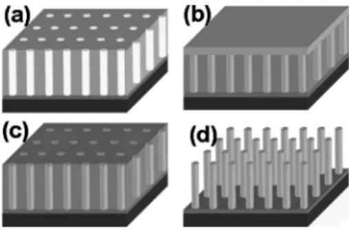
were used as the precursors. ZnO deposition was achieved at 250 ° C for 550 cycles with DEZ pulse time of 1 s, purge time of 1.5 s, H2O pulse time of 1 s, and H2O purge time of 1.5 s. Since surface reaction control occurs in the ALD pro-cess, ZnO can be deposited layer by layer into the AAO nanopores. After deposition, the ZnO film filled the AAO nanopores and covered its surface, as shown schematically in Fig.1共b兲. With slight polishing, the ZnO film on the AAO surface can be removed, as shown schematically in Fig.1共c兲. The final step was to remove the AAO selectively by a so-lution of 0.4 wt % NaOH共aq兲, leaving the ZnO nanorod arrays standing perpendicular to the Si substrate, as shown sche-matically in Fig.1共d兲.
The nanostructure and morphology of the ZnO nanorods were examined by field-emission scanning electron micro-scope 共JSM-6500F兲. Photoluminescence 共PL兲 spectroscopy was performed at room temperature, using a continuous wave He–Cd laser of 325 nm wavelength as the excitation source. The measurements were conducted by simple diode configuration and carried out in a high vacuum chamber at 10−6torr. The distance between the specimen and the anode
a兲Electronic mail: [email protected]
FIG. 1. Schematic diagram of fabricating ZnO nanorod arrays:共a兲 AAO on a Si substrate,共b兲 after the deposition of ZnO by ALD, 共c兲 after the polish-ing step, and共d兲 after the selective etching of the AAO template.
APPLIED PHYSICS LETTERS 90, 033104共2007兲
0003-6951/2007/90共3兲/033104/3/$23.00 90, 033104-1 © 2007 American Institute of Physics
This article is copyrighted as indicated in the article. Reuse of AIP content is subject to the terms at: http://scitation.aip.org/termsconditions. Downloaded to IP: 140.113.38.11 On: Thu, 01 May 2014 00:41:39
was about 100m, and it was controlled by a precise screw meter. The specimen was biased with a positive voltage sweeping from 0 to 1000 V at room temperature to extract electrons from the ZnO emitters. A voltage source, Keithley 237, was used for providing the sweeping electric field共E兲 and monitoring the emission current density共J兲.
With the aid of AAO and ALD, highly ordered and ver-tical arrays of ZnO nanorods can be prepared. Figure 2共a兲
shows the plan-view scanning electron microscopy 共SEM兲 image for the AAO nanopores on a Si substrate before the deposition of ZnO. The AAO nanopores were 70 nm in di-ameter and their periodicity was 90 nm. After the deposition of ZnO by ALD at 250 ° C, all the nanopores were filled by the ZnO film and the film became continuous, as shown in the plan-view SEM image in Fig.2共b兲. After polishing and selective etching, the ZnO nanorods remained perpendicular to the Si substrate and could be observed clearly, as illus-trated in the plan-view SEM image in Fig.2共c兲. We observe that the AAO nanopores can be filled completely by ZnO. It is worth noting that the nanorods remained separate and did not touch each other after the removal of the AAO template. Figure 2共d兲 shows the cross-sectional view of the ZnO ar-rays. The height of the nanorods was 470 nm. Some of the ZnO nanorods near the front edge were broken during the cleavage process for the preparation of cross-sectional SEM samples. ZnO nanorods with uniform height can be fabri-cated by this approach. Further, they were vertically aligned to each other. Therefore, this approach demonstrates an ex-cellent way for fabricating self-organized, uniform height, and straight ZnO nanorod arrays on Si substrates.
Compared with the ZnO film prepared by ALD without template, the PL of ZnO nanorods was significantly en-hanced. Figure 3 shows the PL spectra for a 180-nm-thick ZnO film and the ZnO nanorod arrays. The film was pre-pared at the same conditions of 550 cycles and 250 ° C. For both the ZnO film and nanorods, strong excitation emission was observed in the ultraviolet region with a peak at 379 nm. However, the PL intensity for the nanorods was much higher. Shen et al.18studied the PL spectrum of ZnO nanorod arrays and suggested that both photon-to-electron conversion effi-ciency and photonic performance were enhanced because of decreasing diameters and increasing surface areas for nano-rod configuration. As a result, ZnO nanonano-rods exhibited
higher PL intensity than that of the ZnO film. From the PL spectrum, it is found that ZnO films had red visible emission located around 625 nm. In contrast, the nanorod arrays pos-sessed a blue/green luminescence centered around 480 nm. From the literature,19–21 the peak at 480 nm is indicative of transitions between oxygen vacancy and interstitial oxygen, common lattice defects related to oxygen and zinc vacancies. With the Ti film serving as the adhesion layer, better quality of ZnO nanorods can be fabricated. As reported by Kim et
al.,22the Ti layer may react with the deposited ZnO to form Zn2TiO4, which has the same crystal structure of wurtzite
and has small lattice mismatch with ZnO. The mismatch may be as small as 0.722% for ZnO 共110兲 on Zn2TiO4 共202兲.
Nevertheless, the orientations of the nanorods in this study are not clear at this moment, and further study is required to clarify this issue.
Furthermore, these ZnO nanorods possess excellent field-emission properties. Figure 4 shows the emission cur-rent density against the applied field for these ZnO nanorod arrays. The turn-on field and the threshold field in this letter were defined as the electric field required to produce current densities of 10A cm−2 and 10 mA cm−2, respectively. A
turn-on field of 6.5 Vm−1was obtained for these ZnO
na-norods. The field-emission data were analyzed using the
FIG. 2. SEM images showing共a兲 AAO template before the deposition of ZnO,共b兲 after the deposition of ZnO at 250 °C by ALD, 共c兲 plan view of ZnO nanorods after removal of the AAO template, and共d兲 cross-sectional view of ZnO nanorods in共c兲. Every ZnO nanorod stands perpendicular to the Si substrate.
FIG. 3. Room-temperature PL spectra for ZnO nanorod arrays and ZnO film on Si substrates.
FIG. 4. Measured field-emission current density as a function of the electric field applied to ZnO nanorod arrays. The inset shows the corresponding Fowler-Nordheim plots.
033104-2 Yang et al. Appl. Phys. Lett. 90, 033104共2007兲
This article is copyrighted as indicated in the article. Reuse of AIP content is subject to the terms at: http://scitation.aip.org/termsconditions. Downloaded to IP: 140.113.38.11 On: Thu, 01 May 2014 00:41:39
Fowler-Nordheim model.23The total current I as a function of the local field at the emitter surface F is approximated by
I⬀共F2/⌽兲exp共−B⌽3/2/ F兲, with B=6.83⫻109V m−1eV−3/2,
and⌽ is the work function of ZnO, which is 5.3 eV. F is usually taken as F =E =V / d, where V is the applied
po-tential, d is the distance between anode and sample,is the field enhancement factor, and E = V / d is the macroscopic field. The inset of Fig.4shows the Fowler-Nordheim plot for the fabricated ZnO nanorods. By plotting ln共1/V2兲 against
1 / V, a straight line was obtained for the nanorods. The linear behavior of this plot indicates that these nanorods possess field-emission behavior that follows the Fowler-Nordheim description quite well. According to previous studies,15,24 field-emission properties including low emission threshold and high current density will be greatly improved if the 1D nanostructures are perfectly aligned and stay perpendicular to their substrate. For the nanorods fabricated by this ap-proach, almost every single nanorod grew perpendicularly to the Si substrate. In addition, owing to the AAO template, the nanorods did not touch each other, resulting in extremely low screen effect. As a result, these ZnO nanorods demonstrate excellent field-emission properties that pose substantial po-tential for possible application in photoelectronic devices.
In summary, high-quality self-aligned ZnO nanorods have been prepared on Si substrate using the AAO template and ALD process on Si substrates without any catalyst or seed layer at temperature as low as 250 ° C. Results from PL spectrum indicated that a strong excitation emission was ob-served at 379 nm and a blue/green luminescence was located around 480 nm. Field-emission measurements on the ZnO nanorods showed a low turn-on field emission of 6.5 Vm−1 at a current density of 10A cm−2. The observed excellent
field-emission quality may be attributed to the fact that every nanorod was perpendicular to the Si substrate. This approach provides a well-controlled method for fabricating large-scale self-aligned ZnO nanorods for many important applications in the field of nanotechnology.
The authors would like to thank the National Science Council of the R. O. C. for financial support through Grant No. 94-2623-7-009-007-AT.
1Y. W. Heo, L. C. Tien, D. P. Norton, B. S. Kang, F. Ren, B. P. Gila, and S. J. Pearton, Appl. Phys. Lett. 85, 2002共2004兲.
2Q. Li, V. Kumar, Y. Li, H. Zhang, T. J. Marks, and R. P. H. Chang, Chem. Mater. 17, 1001共2005兲.
3H. Chik, J. Liang, S. G. Cloutier, N. Kouklin, and J. M. Xu, Appl. Phys. Lett. 84, 3376共2004兲.
4M. H. Huang, Y. Wu, H. Feick, N. Tran, E. Weber, and P. Yang, Adv. Mater.共Weinheim, Ger.兲 13, 113 共2001兲.
5Y.-K. Tseng, C.-J. Huang, H.-M. Cheng, I.-N. Lin, K.-S. Liu, and I.-C. Chen, Adv. Funct. Mater. 13, 811共2003兲.
6J. F. Conley, Jr., L. Stecker, and Y. Ono, Nanotechnology 16, 292共2005兲. 7M. S. Arnold, P. Avouris, Z. W. Pan, and Z. L. Wang, J. Phys. Chem. B
107, 659共2003兲.
8Z. L. Wang, J. Mater. Chem. 15, 1021共2005兲.
9Z. W. Pan, Z. R. Dai, and Z. L. Wang, Science 291, 1947共2001兲. 10Y. B. Li, Y. Bando, T. Sato, and K. Kurashima, Appl. Phys. Lett. 81, 144
共2002兲.
11S. Liang, H. Sheng, Y. Liu, Z. Huo, Y. Lu, and H. Shen, J. Cryst. Growth 225, 110共2001兲.
12C. R. Gorla, N. W. Emanetoglu, S. Liang, W. E. Mayo, Y. Lu, M. Wra-back, and H. Shen, J. Appl. Phys. 85, 2595共1999兲.
13S. C. Minne, S. R. Manalis, and C. F. Quates, Appl. Phys. Lett. 67, 3918 共1995兲.
14R. F. Service, Mater. Sci. 276, 895共1997兲.
15M. H. Huang, S. Mao, H. Feick, H. Yan, Y. Wu, H. Kind, E. Weber, R. Russo, and P. Yang, Science 292, 1897共2001兲.
16M. Scharrer, X. Wu, A. Yamilov, H. Cao, and R. P. H. Chang, Appl. Phys. Lett. 86, 1511131共2005兲.
17H. Masuda and K. Fukuda, Science 268, 1466共1995兲.
18X.-P. Shen, A.-H. Yuan, Y.-M. Hu, Y. Jiang, Z. Xu, and Z. Hu, Nanotechnology 16, 2039共2005兲.
19S. Mahamuni, K. Borgohain, B. S. Bendre, V. J. Leppert, and S. H. Ris-bud, J. Appl. Phys. 85, 2861共1999兲.
20J. Q. Hu, X. L. Ma, Z. Y. Xie, N. B. Wong, C. S. Lee, and S. T. Lee, Chem. Phys. Lett. 344, 97共2001兲.
21A. van Dijken, E. A. Meulenkamp, D. Vanmaekelbergh, and A. Meijerink, J. Lumin. 90, 123共2000兲.
22S.-K. Kim, S.-Y. Jeong, and C.-R. Cho, Appl. Phys. Lett. 82, 562共2003兲. 23R. H. Fowler and L. W. Nordheim, Proc. R. Soc. London 119, 173共1928兲. 24Y. Zhang, K. Yu, S. Ouyang, and Z. Zhu, Mater. Lett. 60, 522共2006兲.
033104-3 Yang et al. Appl. Phys. Lett. 90, 033104共2007兲
This article is copyrighted as indicated in the article. Reuse of AIP content is subject to the terms at: http://scitation.aip.org/termsconditions. Downloaded to IP: 140.113.38.11 On: Thu, 01 May 2014 00:41:39