IEEE ELECTRON DEVICE LETTERS, VOL. 20, NO. 4, APRIL 1999 185
A Novel Technology to Form
Air Gap for ULSI Application
Kow-Ming Chang, Ji-Yi Yang, and Lih-Woen Chen
Abstract—In this letter, we develop a novel process to fill the
interline space with air (dielectric constant=== 1). A silicon wafer, whose face is downward, patterned with metal lines, is placed on the top of another silicon wafer coated with dry polyimide. Hydrogen silsesquioxanes (HSQ), FOx-16, is diluted and trickled through the slit between the metal lines and the polyimide. Then the HSQ forms an ultrathin liquid layer on the dry polyimide and contacts with the top of the metal lines. After the liquid HSQ becomes dry, the air gap is formed. The dry polyimide has good adhesion to silicon substrate but not to the dry FOx-16, so we can separate the polyimide from the dry FOx-16 and get the air gap. The liquid property of HSQ and its high selective adsorption between the metal lines and the polyimide are utilized to form the air gap.
Index Terms—Air gap, HSQ, low dielectric constant material,
RC time constant.
I. INTRODUCTION
A
S the feature sizes of ULSI technology continue to shrink, the research for low dielectric constant ( ) to reduce the interconnect RC time constant delay has become a major issue in every generation. The advanced low materials include porous silica, fluorinated inorganic materials, porous organic materials, and various organic materials [1]. These materials are usually deposited by spin-on deposition or chemical vapor deposition techniques. In 0.35- and 0.25- m generations, these low films are already in use [2]. Undoubtedly, to get lowest , air gap is the best choice [3], [4]. However, because of the narrow space between lines, technology such as lift off used for air bridge in compound device is not appropriate in ULSI manufacture. In this letter, we propose a new technology to form air gap. The potential of this technology is that little process time and no vacuum environment is needed to complete the all processes. Compared with previously published papers, this technique gives a better economically sound proposal.II. EXPERIMENTS
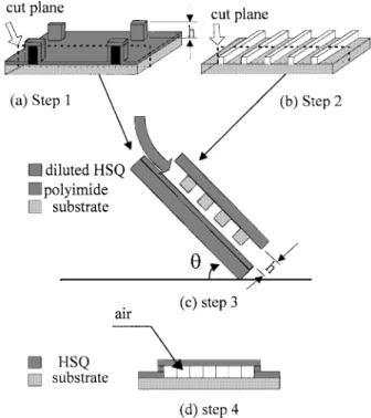
The low material used here is inorganic hydrogen silsesquioxane (HSQ) spin-on material, FOx-16, commercial-ized by the Dow Corning Corporation for intermetal dielectric application. The diluted FOx-16 is the mixture of FOx-16 and its solvent, methyl isobutyl ketone. Fig. 1 is the process flow to
Manuscript received November 28, 1998; revised December 3, 1998. This work was supported by the National Science Council, R.O.C., under Contract NSC 87-2215-E-009-071.
The authors are with the Department of Electronics Engineering and In-stitute of Electronics, National Chiao-Tung University, Hsinchu 300, Taiwan, R.O.C.
Publisher Item Identifier S 0741-3106(99)02499-4.
Fig. 1. Process flow of air gap formation.
form the air gap. First, the polyimide PI2809, commercialized by Dupont Corporation, is spun on a bare patterned silicon wafer. The patterned silicon wafer has some silicon beetle regions whose thickness, , is thicker than the patterned metal lines (1.08 m). This is followed by 3 min hot plate bake at 120 C. The baked polyimide has good adhesion to the bare silicon but not to the diluted FOx-16. With this buffer polyimide, substrate will not contact to the FOx-16. Second, another wafer with patterned metal lines on 500-nm wet oxide is faced downward and put on the top of polyimide coated wafer in step 1 and the two wafers are tilted an angle , e.g., about 45 used here. In this step, the silicon beetle regions should be located far away from the metal lines region to avoid affecting the flowage of FOx-16, for example, the four corners of the patterned metal line. There is a slit produced in this step as shown in Fig. 1(c). The height of the slit is equal to the thickness of silicon beetle region minus the thickness of metal line. This process is operated in one atmospheric pressure. No special gas environment is used. The patterned metal lines are cross fingers structure, and each line is 0.5 cm in length. The metal lines are four layer metals TiN/Al–Si–Cu/TiN/Ti structure, with the thickness of 40, 900, 100, and 40 nm, respectively. There are 500 lines in a test key.
186 IEEE ELECTRON DEVICE LETTERS, VOL. 20, NO. 4, APRIL 1999
(a)
(b)
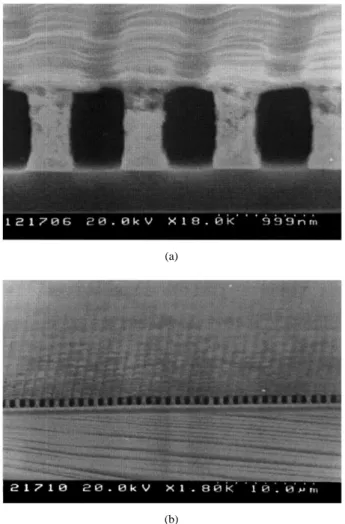
Fig. 2. (a) SEM picture of air gap. (b) SEM picture of air gap in large area.
Third, the diluted FOx-16 is trickled through the slit between the polyimide and the patterned metal lines to form a thin fluid layer on the polyimide at room temperature. This thin fluid layer touches the polyimide and the top of the metal lines concurrently. Finally, after the diluted FOx-16 became dry, we removed the buffer polyimide by organic solvent such as ACE or just by scratching the polyimide film from the dry FOx-16 or let it to be separated from the dry FOx-16 automatically at follow-up thermal cycle. Thus, the air gap was formed and the total processes were complete. The experiments studied here are operated by manual. The automatic equipment under developing is already conceptually patented.
III. RESULTS AND DISCUSSION
The SEM picture is shown in Fig. 2(a) and (b). In Fig. 2(a), the bright regions in the photograph are the metal lines and the thin insulator film forms the “bridge layer” over interconnect metal lines. The gray regions between the metal lines are “air.” The “air” regions are formed by the mixture of the volatile matter of FOx-16 and the surrounding air in process. The metal lines width is 0.4 m and the spacing is 0.8 m. The final curing temperature is 400 C for 30 min. There are no cracks observed and no additional HSQ on the sidewall of the metal lines. According the simple electrical model [4], the parasitic capacitance between closely spaced metal lines will have the
Fig. 3. The wire-to-wire isolation characteristics of Plasma-TEOS ILD and the air gap.
Fig. 4. Comparison of the wire-to-wire parasitic capacitance of plasma-TEOS ILD and the air gap.
lowest effective dielectric constant. The bridge layer formed from the dry HSQ is about 100 nm thick.
Fig. 2(b) is also the SEM picture of the air gap. This picture shows the excellent planarization characteristics over a large area. The metal line width is 0.5 m and the spacing is 0.5 m. Figs. 3 and 4 are the basic electrical characterization data. Fig. 3 shows the leakage currents of the air gap and PECVD isolation under different applied voltages. It is seen that under 5-V operation, the leakage current of the air gap is smaller than that of PECVD oxide isolation. Even at higher voltage, such as 30 V, the air gap still has the smaller leakage current. Fig. 4 shows the parasitic capacitance of the air gap and the reference sample. The test structure is 0.7 m/0.5 m spacing/width. The parasitic capacitance of a reference sam-ple using PECVD oxide as interlayer dielectric constant is 34 fF/mm, which is about four times higher than that of the air gap, 8.4 fF/mm. The measured parasitic capacitance is the average value of many measurements. These results show that the parasitic capacitance can be largely decreased with air gap isolation.
IV. CONCLUSION
A novel technology at reducing the parasitic capacitance of the interconnect wires is developed in this paper. The approach presents another way to allow the use of air as
CHANG et al.: NOVEL TECHNOLOGY TO FORM AIR GAP 187
the dielectric, thus achieving the lowest effective dielectric constant physically possible. This technique also provides simple and rapid advantage to integrated circuit process. With the well-known lowest dielectric constant, for future ULSI development, we believe that the air gap will play a very important role.
REFERENCES
[1] B. Zhao, S. Q. Wang, S. Anderson, R. Lam, M. Fiebig, P. K. Vasudev, and T. E. Seidel, “On advanced inter connect using low dielectric
constant material as inter-level dielectrics,” in Proc. Mat. Res. Soc.
Symp., 1996, vol. 427, p. 415.
[2] H. Oyamatsu, M. Kinugawa, and M. Kakumu, “A high-performance MOSFET design with highly controllable gate length and low-power RC delay multilevel interconnects technology for high speed logic devices,” in IEDM Tech. Dig., 1995, p. 705.
[3] M. B. Anand, M. Yamada, and H. Shibata, “NURA: A feasible, gas-dielectric interconnect process,” in 1996 Symp. VLSI Tech. Dig. Tech.
Papers, p. 82.
[4] J. G. Fleming and E. Roherty-Osmun, “Use of air gap structures to lower interlever capacitance,” in Dielectrics for ULSI Multilevel