Effect of three-dimensional current and temperature distributions on void formation
and propagation in flip-chip solder joints during electromigration
S. W. Liang, Y. W. Chang, T. L. Shao, Chih Chen, and K. N. Tu
Citation: Applied Physics Letters 89, 022117 (2006); doi: 10.1063/1.2220550
View online: http://dx.doi.org/10.1063/1.2220550
View Table of Contents: http://scitation.aip.org/content/aip/journal/apl/89/2?ver=pdfcov Published by the AIP Publishing
Articles you may be interested in
Influence of Cu column under-bump-metallizations on current crowding and Joule heating effects of electromigration in flip-chip solder joints
J. Appl. Phys. 111, 043705 (2012); 10.1063/1.3682484
Effect of void propagation on bump resistance due to electromigration in flip-chip solder joints using Kelvin structure
Appl. Phys. Lett. 91, 132113 (2007); 10.1063/1.2790376
Effect of Al-trace degradation on Joule heating during electromigration in flip-chip solder joints Appl. Phys. Lett. 90, 082103 (2007); 10.1063/1.2644061
Investigation of void nucleation and propagation during electromigration of flip-chip solder joints using x-ray microscopy
Appl. Phys. Lett. 89, 262106 (2006); 10.1063/1.2425040
Three-dimensional simulation on current-density distribution in flip-chip solder joints under electric current stressing
J. Appl. Phys. 98, 044509 (2005); 10.1063/1.2000667
This article is copyrighted as indicated in the article. Reuse of AIP content is subject to the terms at: http://scitation.aip.org/termsconditions. Downloaded to IP: 140.113.38.11 On: Thu, 01 May 2014 01:54:18
Effect of three-dimensional current and temperature distributions
on void formation and propagation in flip-chip solder joints
during electromigration
S. W. Liang, Y. W. Chang, T. L. Shao, and Chih Chena兲
Department of Material Science and Engineering, National Chiao Tung University, Hsin-chu, 30050 Taiwan, Republic of China
K. N. Tu
Department of Materials Science and Engineering, UCLA, Los Angeles, California 90095-1595
共Received 5 February 2006; accepted 23 May 2006; published online 13 July 2006兲
Effect of three-dimensional current distribution on void formation in flip-chip solder joints during electromigration was investigated using thermoelectrical coupled modeling, in which the current and temperature redistributions were coupled and simulated at different stages of void growth. Simulation results show that a thin underbump metallization of low resistance in the periphery of the solder joint can serve as a conducting path, leading to void propagation in the periphery of the low current density region. In addition, the temperature of the solder did not rise significantly until 95% of the contact opening was eclipsed by the propagating void. © 2006 American Institute of Physics. 关DOI:10.1063/1.2220550兴
Electromigration has become a critical reliability issue for high-density solder joints in flip-chip technology.1,2 Electromigration-induced failures and mean time to failure 共MTTF兲 of flip-chip joints have been investigated for both eutectic SnPb and Pb-free solders.3–10It was found that voids were formed inside the solder adjacent to the underbump metallization 共UBM兲,4 and propagated along the interface between the solder and the UBM, causing opening failure of the joints when the voids eclipsed the entire contact opening. However, the mechanism of void nucleation and growth and especially the corresponding change of current distribution in the solder joint due to void formation are unclear. In particu-lar, it is unknown why some voids are formed at the periph-ery of the UBM opening under the dielectric, where the cur-rent density is low.8,11In Blech structure of Al stripes, Tu et
al. proposed that resistive vacancy might move to the low
current density region to form voids due to the high gradient of current density, which was as high as 1010 A / cm3.12
How-ever, for flip-chip solder joint, the gradient is estimated to be only 1.33⫻106A / cm3owing to its large dimension.8
There-fore, the growth of voids in the periphery of the UBM open-ing, which is located at the low current density region, may not be driven by the gradient of current density. In this letter, three-dimensional finite element method was employed to simulate the effect of void formation on redistribution of current density and temperature in a flip-chip solder joint, especially in the periphery area where a low-resistance thin-film UBM exists.
Three-dimensional 共3D兲 thermoelectrical coupled simu-lation was carried out by finite element analysis to find out the current density and temperature redistributions in our test samples.13The model used was a SOLID69 eight-node hexa-hedral coupled field element withANSYSsoftware. The elec-trical and thermal resistivities of the materials as well as the boundary conditions used in this modeling followed those of
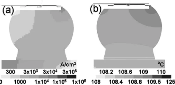
our previous study.13 In our samples, the diameters of the passivation opening and the UBM opening were 85 and 120m, respectively. Figure 1共a兲 shows the cross-sectional view of the current density distributions before void growth when 0.28 A was applied to the bump. The Al trace, the UBM in the chip side, and the metallization in the substrate were ignored. It was found that the current crowded into the solder bump in the passivation opening. The current crowd-ing behavior near the entrance of the Al trace can be clearly demonstrated. The maximum current density reached 5.42 ⫻104A / cm2, which is about 22 times higher than the
aver-age value. It is proposed that this local high current density was responsible for the initial void formation due to flux divergence.4,6Figure 1共b兲 illustrates the temperature distribu-tion before void formadistribu-tion. The maximum temperature inside the solder bump was 109.6 ° C; therefore, the increase in temperature due to Joule heating was only 9.6 ° C. The tem-perature was quite uniform inside the bulk of the solder.
In stage I, a semicylindrical void, 45.5m in diameter and 13.0m in height, was formed inside the solder near the entrance of the Al trace. The current redistributed due to void formation, and the maximum current density occurred in the solder near the upper left corner of the periphery of the UBM opening under the Al trace. As shown in Fig. 2共a兲, void
for-a兲Author to whom correspondence should be addressed; electronic mail:
FIG. 1. 共a兲 Cross-sectional view of current density distribution in solder joint before void formation;共b兲 corresponding cross-sectional view for tem-perature distribution.
APPLIED PHYSICS LETTERS 89, 022117共2006兲
0003-6951/2006/89共2兲/022117/3/$23.00 89, 022117-1 © 2006 American Institute of Physics
This article is copyrighted as indicated in the article. Reuse of AIP content is subject to the terms at: http://scitation.aip.org/termsconditions. Downloaded to IP: 140.113.38.11 On: Thu, 01 May 2014 01:54:18
mation resulted in redistribution of current in two ways. First, current may drift farther along the Al trace, passing the void, and entered the solder. Second, the current may drain down to the solder through the surrounding UBM/ intermetallic layer共IMC兲 layer. It is intriguing that the UBM/ IMC layers served as a current path, directing the current into the upper left corner of the periphery of the UBM open-ing. Since the UBM/IMC layers have much higher electromi-gration resistance,2 voids are formed mainly inside the sol-der. It is clear that the solder on the left of the void has higher current density than that under the passivation open-ing. Therefore, voids may propagate toward the solder in the UBM periphery. Compared with that shown in Fig. 1, the maximum current density inside the solder has been reduced to 4.43⫻104A / cm2 due to void formation. On the other
hand, the temperature inside the solder decreased slightly to 109.5 ° C, which was 0.1 ° C lower than that before void formation, as illustrated in Fig. 2共b兲. This may be attributed to the smaller crowding effect as a result of void formation. Since the maximum current density occurred near the periphery of the UBM opening, we assume that the void propagates toward the left-hand-side periphery, as illustrated in Fig. 3共a兲. The void depleted 50% of the UBM opening, which is denoted as stage II. Since the UBM/IMC layers still serve as a current path, the void may be able to propagate to the edge of the solder bump. Therefore, we postulate that the growth of void in the low current density region under the periphery of the UBM opening is mainly attributed to current redistribution, not to the gradient of current density. The maximum current density inside the solder bump reduced further to 4.04⫻104A / cm2 due to void formation. Figure
3共b兲 shows the corresponding temperature distribution in the solder bump. The maximum temperature in the solder was 109.3 ° C, which was 0.2 ° C lower than that in stage II. Again, this may be due to the smaller crowding effect in the solder joint at this stage. Although there was a slight increase
in temperature in the Al pad, the temperature inside the sol-der did not alter much at this stage. From the results reported by Gee et al.,11 the shape of the void may resemble a pan-cake shape for solder joints with thin-film UBM. In addition, due to the limitation of our simulation modeling, semicylin-drical voids were adopted in this study. However, whether it is circular, semicircular, or irregular remains unclear at this moment, and needs further experimental investigation.
The void was then assumed to propagate to fill 80.5% of the UBM opening, as shown in Fig. 4共a兲. It is denoted as stage III. The current entered the joints through a smaller contact area, causing an increase in maximum current den-sity. It rose to 8.70⫻104A / cm2, and almost the whole
pas-sivation opening experienced current density higher than 1.0⫻104A / cm2. Therefore, void propagation would
expe-dite in this stage. The maximum temperature in the solder bump increased to 109.4 ° C because of the higher current crowding effect at this stage, as shown in Fig. 4共b兲. In the absence of current flowing through the solder in the left-hand side of the joint, the temperature on the right-hand side was higher than that on the left-hand side. However, there was still no obvious temperature increase in the solder close to the entrance point of the current into the solder.
The solder in the passivation opening was completely depleted at this final stage, leaving a small amount of solder near the periphery of the UBM opening, as illustrated in Fig. 5共a兲. There was approximately 4.0% of contact area left for conducting the current at this stage. With further decrease in contact area, the maximum current density became 1.69 ⫻105A / cm2. The UBM/IMC layers served as a conducting
path to direct the current to the remaining solder. Hence, the remaining solder near the periphery of the UBM opening could be completely depleted and failure followed. Figure 5共b兲 shows the temperature distribution at this stage. The maximum temperature in the solder bump was 110.4 ° C, which was 0.8 ° C higher than that before void formation.
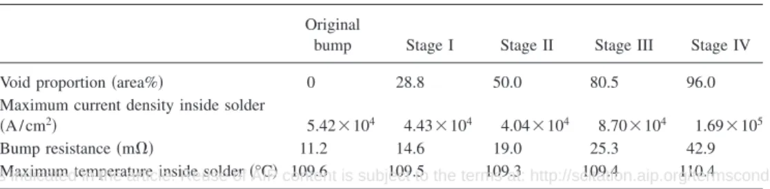
TABLE I. The simulated maximum current density inside the solder, the corresponding crowding ratio as well as the bump resistance at each stage.
Original
bump Stage I Stage II Stage III Stage IV
Void proportion共area%兲 0 28.8 50.0 80.5 96.0
Maximum current density inside solder
共A/cm2兲 5.42⫻104 4.43⫻104 4.04⫻104 8.70⫻104 1.69⫻105
Bump resistance共m⍀兲 11.2 14.6 19.0 25.3 42.9
Maximum temperature inside solder共°C兲 109.6 109.5 109.3 109.4 110.4
FIG. 2. 共a兲 Cross-sectional view of current density distribution in solder joint at stage I; 共b兲 corresponding cross-sectional view for temperature distribution.
FIG. 3. 共a兲 Cross-sectional view of current density distribution in solder joint at stage II; 共b兲 corresponding cross-sectional view for temperature distribution.
022117-2 Liang et al. Appl. Phys. Lett. 89, 022117共2006兲
This article is copyrighted as indicated in the article. Reuse of AIP content is subject to the terms at: http://scitation.aip.org/termsconditions. Downloaded to IP: 140.113.38.11 On: Thu, 01 May 2014 01:54:18
Our simulation also shows that bump resistance in-creased gradually in the first three stages, and then inin-creased rapidly in the final stage, as shown in Table I. Bump resis-tance was defined as the decrease in voltage between the entrance point of the Al trace into the Al pad共disk兲 and the junction point of the Cu line with the solder joint. In stage I, the bump resistance increased from 11.2 to 14.6 m⍀. It in-creased to 19.0 and 25.3 m⍀ in stages II and III, respec-tively. It rose to 42.9 m⍀ in stage IV. This increase in bump resistance may also enhance the local Joule heating effect. However, no significant local Joule heating was found in the thermal simulation up to stage IV. This may be attributed to the fact that the major heating source was the Al trace.14In our model, the total resistance of the Al trace was about 1800 m⍀. Consequently, the increase in bump resistance was quite small compared with that of the Al trace. In addi-tion, the increase in bump resistance was mainly due to the following manner: owing to void formation, the current needed to drift farther in the Al pad共disk兲, and then flowed down to the solder bump. Therefore, the local Joule heating in the Al pad 共disk兲 increased when voids were formed. Since there was good heat dissipation in the Si side, the increase in temperature due to void formation was quite small. Nevertheless, the increase might be higher when larger current was applied, since the overall Joule heating would be significantly higher at higher stressing current.
In summary, we have employed the 3D finite element method to simulate the current and temperature redistribu-tions due to the formation and propagation of a pancake-shape void in solder joints during electromigration. It is pro-posed that current redistribution is the main reason accounting for void formation and propagation, especially the propagation into the low current density region below the contact passivation. It is found that UBM provided a con-ducting path for current to go below the passivation, and it
directed the current to the periphery of the solder joint, which is in agreement with the experimental observation of void formation in those regions. Increase in temperature due to void formation was not significant since the major heat source was the Al trace and the applied current was as low as 0.28 A.
The authors would like to thank National Science Coun-cil of Taiwan of the Republic of China for the financial sup-port through Grant No. NSC 95-2218-E-009-022. In addi-tion, the assistance on simulation facility from the National Center for High-performance Computing共NCHC兲 in Taiwan is highly appreciated.
1International Technology Roadmap for Semiconductors, Semiconductor
Industry Association, San Jose, CA, 2003.
2K. N. Tu, J. Appl. Phys. 94, 5451共2003兲.
3C. Y. Liu, Chih Chen, C. N. Liao, and K. N. Tu, Appl. Phys. Lett. 75, 58
共1999兲.
4Everett C.C. Yeh, W. J. Choi, and K. N. Tu, Appl. Phys. Lett. 80, 4
共2002兲.
5W. J. Choi, E. C. C. Yeh, and K. N. Tu, J. Appl. Phys. 94, 5665共2003兲. 6J. W. Nah, K. W. Paik, J. O. Suh, and K. N. Tu, J. Appl. Phys. 94, 7560
共2003兲.
7J. D. Wu, P. J. Zheng, C. W. Lee, S. C. Hung, and J. J. Lee, Microelectron.
Reliab., 46, 41共2006兲.
8T. L. Shao, Y. H. Chen, S. H. Chiu, and Chih Chen, J. Appl. Phys. 96,
4518共2004兲.
9J. W. Jang, L. N. Ramanathan, J. K. Lin, and D. R. Frear, J. Appl. Phys. 95, 8286共2004兲.
10H. Ye, C. Basaran, and D. Hopkins, Appl. Phys. Lett. 82, 7共2003兲. 11L. Zhang, S. Ou, J. Huang, K. N. Tu, S. Gee, and L. Nguyen, Appl. Phys.
Lett. 88, 012106共2006兲.
12K. N. Tu, C. C. Yeh, C. Y. Liu, and Chih Chen, Appl. Phys. Lett. 76, 988
共2000兲.
13S. H. Chiu, T. L. Shao, Chih Chen, D. J. Yao, and C. Y. Hsu, Appl. Phys.
Lett. 88, 022110共2006兲.
14T. L. Shao, S. H. Chiu, Chih Chen, D. J. Yao, and C. Y. Hsu, J. Electron.
Mater. 33 1350共2004兲. FIG. 4. 共a兲 Cross-sectional view of current density distribution in solder
joint at stage III.;共b兲 corresponding cross-sectional view for temperature distribution.
FIG. 5. 共a兲 Cross-sectional view of current density distribution in solder joint at stage IV;共b兲 corresponding cross-sectional view for temperature distribution.
022117-3 Liang et al. Appl. Phys. Lett. 89, 022117共2006兲
This article is copyrighted as indicated in the article. Reuse of AIP content is subject to the terms at: http://scitation.aip.org/termsconditions. Downloaded to IP: 140.113.38.11 On: Thu, 01 May 2014 01:54:18