Abstract—Stepped-impedance resonators with different dimen-sions are used to design bandpass filters with a dual-passband response, as well as good rejection levels in the extended upper stopband. To achieve the goal, the resonators are designed to have two identical leading resonant frequencies, but dispersed higher order ones to make spurious peaks have low levels and small band-widths. The stopband is then extended and the rejection levels are enhanced by collocating transmission zeros with the unwanted peaks. The zeros are tuned by adjusting the coupling lengths of the coupled stages and sliding the tap positions of the dual-band transformers along the end resonators. Measured results of two experimental circuits show a rejection level of 30 dB up to more than eight times the first passband frequency can be obtained. The measured data have good agreement with the simulation.
Index Terms—Bandpass filter, dual band, impedance trans-former, rejection band, stepped-impedance resonator.
I. INTRODUCTION
D
ESIGN OF dual-band RF devices has become an impor-tant issue due to recent rapid progress of multiband wire-less communication systems, e.g. the global system for mo-bile communications (GSM) 900/1800 cellular phones and the 802.11a/b/g wireless local area networks. Bandpass filters are an essential device in the RF front ends of both the receiver and transmitter. Recently, many new dual-band bandpass filters have been proposed [1]–[8]. In [1], compact hairpin resonators are used to realize two quasi-elliptic function passbands. In [2], the dual-passband response is realized by stepped-impedance resonators in the parallel-coupled configuration. The cross-cou-pled filter in [3] has excellent stopband performance since it has a zero on the high-frequency side of each passband. The design in [4] uses open-loop ring resonators based on both magnetic and electric coupling structures. In [5] and [6], the two opera-tion frequencies are controlled by attaching an open stub to a resonator. In [7], two perturbed ring resonators are employed to obtain the dual-mode dual-band responses. The center frequen-cies and fractional bandwidths of both passbands can be inde-pendently tuned to desired specifications. In [8], the dual-band filter is designed with combline coupled quarter-wave stepped-impedance resonators.Manuscript received June 18, 2008; revised December 10, 2008. First pub-lished March 16, 2009; current version pubpub-lished April 08, 2009. This work was supported in part by the Ministry of Education under the ATU Program and by the National Science Council, Taiwan, under Grant NSC 95-222-E-009-037-MY2 and Grant NSC 96-2221-E-009-245.
The authors are with the Department of Communication Engineering, Na-tional Chiao Tung University, Hsinchu 300, Taiwan (e-mail: [email protected]. edu.tw).
Color versions of one or more of the figures in this paper are available online at http://ieeexplore.ieee.org.
Digital Object Identifier 10.1109/TMTT.2009.2015040
An ideal bandpass filter is expected to be free of spurious. The spurious passbands are, however, one of the natures of distributed networks. Recently, suppressing these unwanted re-sponses has been a hot topic, e.g., [9]–[14]. For parallel-coupled microstrip filters, the spurious peaks arise at all harmonics of the design frequency . Both the corrugated structure [9] and the over-coupled stage [10] are good approaches for eliminating the peak at . The coupling length of a coupled stage can be tuned at to allocate a zero at ( ). When a filter consists of a cascade of such stages with different , the leading several unwanted spurious peaks can be effectively suppressed [11]. The filters based on the wiggly-line [12] and stepped-impedance resonators [13] have an extended upper stopband up to more than . In [13], two transmission zeros created by tapped input/output are incorporated into the design to eliminate the second and third resonances. In [14], multi-spurious suppression is achieved by choosing the constitutive resonators having identical passband frequency, but staggered higher order resonances.
There have been few dual-band filters incorporated with ex-tension of the upper stopband [15], [16]. In [15], it is found that the distances among the higher order resonances of the hairpin resonators are limited so that the stopband performance needs improving. The design in [16] uses end-coupled stepped-impedance resonators to achieve excellent stopband rejection. In this paper, starting from the idea in [14], dual-band filters are de-signed with dissimilar stepped-impedance resonators. Multiple transmission zeros are tuned by adjusting the coupling lengths of the constitutive stages, and by sliding the tap positions on the end resonators [13] to eliminate the higher order resonances so that an improved upper stopband can be achieved. It is noted that the impedance transformer considered here is for dual-band purpose [17] instead of for a single passband, as in [13]. The geometric parameters of the dual-band transformers must be changed when the tap point is moved.
This paper is organized as follows. Section II explains the choice of the geometric dimensions of the stepped-impedance resonators based on their resonant properties. The design pro-cedure of a parallel-coupled filter with a dual-band response is briefly reviewed. Section III investigates the tuning of the trans-mission zeros. Section IV presents measured results of two ex-perimental circuits. Section V discusses the optimization of cir-cuit parameters. Section VI then draws a conclusion.
II. RESONATORGEOMETRY ANDDUAL-BAND BANDPASSFILTERDESIGN
Fig. 1 shows the layout of a fourth-order dual-band bandpass filter with tapped input/output. The four stepped-impedance res-0018-9480/$25.00 © 2009 IEEE
Fig. 1. Layout of a fourth-order dual-band parallel-coupled stepped-impedance resonator bandpass filter.
TABLE I
GEOMETRICDIMENSIONS OF THEFOURSTEPPED-IMPEDANCERESONATORS
onators may have different dimensions. For the th resonator, the length and characteristic impedance of the two end sections are and (linewidth ) and those of the middle sec-tion are and (linewidth ), respectively. The geo-metric dimensions of the resonators are determined as follows. Suppose we are designing a dual-band filter with passbands at GHz and GHz. The resonant conditions for the resonators given in [2] and [13] can be invoked to calcu-late their resonant spectrum. Based on the normalized resonant spectrum like that in [13, Fig. 3], one can draw a horizontal
line at to determine the length and
impedance ratios, i.e., and , of the resonators. There is one degree of freedom in choosing the solutions. The ratio , however, will be altered if is changed. When GHz is given, the values of and are then fixed. In our design, the choice of the solutions is to stagger their higher order resonances as much as possible. Table I lists the geometric parameters of the four chosen resonators.
The filter in Fig. 1 has three parallel-coupled stages. Given the bandwidths and ripple levels of the two passbands, the cou-pling length and the gap size , or , can be determined by the bandwidth design graph [2] shown in Fig. 2. The three graphs are constructed as follows. Let (horizontal axis) and (vertical axis) denote the fractional bandwidths at and , respectively. The key idea for establishing the graphs is that the coupling coefficient of each stage is proportional to the bandwidth at each passband. Given and , the coupling coefficients at and can be obtained by simulation [2]. The solutions of the dual-band filter are then the overlapped region of three graphs expanded by various sets of and . For this particular example, it can be observed from Fig. 2 that the solu-tions are dominated by the design graph of the first stage since it is a narrow strip region locating around the centers of the other two graphs. The narrow strip area indicates that when one frac-tional bandwidth is chosen, the room for choosing the other one is small. Design graphs for circuits of higher orders can be es-tablished in a similar way [18].
The last step is to design a dual-band transformer [17] to adapt the singly loaded quality factor of each end resonator to the specified bandwidths at and . Fig. 3(a) plots simulated
Fig. 2. Bandwidth design graphs for a trial dual-band filter. Dimensions of the resonators are in Table I. Numbers in parentheses with black rectangular dots are for the first stage, and the circular dots are for the third stages. Substrate: " = 2:2, thickness = 0:508 mm.
Fig. 3. Simulation responses of fourth-order dual-band filters. (a) Four test fil-ters with identical resonators. Filterk uses the kth resonators in Table I. (b) Filter with four dissimilar resonators (filter A). The dimensions of the resonators are in Table I. All filters are designed with ripple= 0:1 dB, 1 = 12:5%, and 1 = 3:5%. Substrate: " = 2:2 and thickness = 0:508 mm.
responses of four test filters; each of them is designed with four identical resonators. Fig. 3(b) plots the response of a trial filter (filter A) with all the four dissimilar resonators listed in Table I.
All five filters are designed with ripple dB, , and . The simulation is carried out via the software package IE3D [19]. The geometric parameters, including those of the dual-band transformers, of the five circuits are given in Table II. In Fig. 3(a), each filter has 3–5 peaks before 20 GHz with a level up to 3 1 dB. In Fig. 3(b), with incoherence of the higher order resonances of the four resonators, the response of filter A shows more spurious peaks, but all their peak insertion losses are below 9.8 dB. In addition, the spurious passbands show much narrower bandwidths than the previous four circuits before 15 GHz . This point is important, based on our experience shown in [13, Fig. 9(a)] since a single zero may not be sufficient for suppressing a spurious with a wide bandwidth. Although the peak at 18.5 GHz has a comparable bandwidth with those in Fig. 3(a), its level is 15 dB. Thus, the choice of dissimilar resonators to construct the filter will save much effort of the following work on extending the upper stopband and improving the rejection levels. Note that filter A has good in-band insertion and return losses in both passbands.
III. TUNING OFTRANSMISSIONZEROS
A. Coupling Length
Now consider how to improve the stopband performance of filter A. A uniform coupled stage of long possesses inherent zeros at the frequencies where the coupling length is a multiple of [10], [11]. In [11], transmission zeros are tuned at , , and ( is the design frequency) with changing the coupling lengths around , , and , respectively. Note that when the coupling length is changed, the gap size must be altered at the same time to compensate the coupling coefficient of the stage specified by the synthesis formulas.
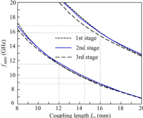
The three stages in Fig. 1 surely also possess transmission zeros of the same property. The prediction of the zeros by formulation with the transmission line theory, however, will be lengthy and tedious since asymmetric coupled lines are involved. One possible easy way is to calculate the data by the electromagnetic (EM) simulation. Fig. 4 plots the zeros versus the length of the three stages. Based on the sizes of the three ’s given in the design graphs in Fig. 2, the variations of the zeros are investigated only when coupling lengths are between 8–20 mm. It can be anticipated that the zero frequencies are insensitive to the gap size . As shown in Fig. 4, two sets of zeros before 20 GHz can be used for the spurious suppression. The zeros in the higher frequency set are about 10% less than twice those of the lower one. For example, when mm,
Fig. 4. Transmission zeros of the three coupled stages versus their coupling lengths.
Fig. 5. Schematic of the dual-band impedance transformer.
the two zeros are at 10.1 and 18.0 GHz. Note that for a uniform coupled stage, the frequency of the second zero will be twice that of the first one. The zeros decrease as is increased, as expected, and can be continuously tuned. It is important to note that the two variables of each stage ( and ) have been determined when the bandwidths at and are specified [2]. Thus, if is changed for allocating a zero at certain frequency, one or two fractional bandwidths will also be changed, and hence, the and values of the other two stages also have to be adjusted accordingly. This reveals that the tuning of the zeros will also limit the choices of the two bandwidths and that the design graphs indeed play a critically important role in the tuning process.
B. Tapped Input/Output Structure
The zeros created by the tapped input/output are also tunable by changing the distances and in Fig. 1. Fig. 5 plots the tapped input structure with more detailed circuit parameter notations. The structure for the output coupling can be analyzed in a similar fashion. The zero occurs at the frequency where is equivalent to a - or -section uniform line. For the dual-band impedance transformer in Fig. 5, at , or , the impedance looking to the source/load seen at the tap point has to meet the requirement of the value of the tapped resonator by [2]
Fig. 6. Solutions of the input dual-band transformer and the transmission zeros versus the tap positiond (Fig. 1).
where and are the element values of the low-pass prototype and and are, respectively, the fractional bandwidth and the input susceptance of the resonator seen at the tap point at . The expression of can be referred to [13]. On the other hand, the impedance can be formulated in terms of , , , and by successively applying twice the following well-known input impedance equation of a loaded transmission line section
(2) where is the load impedance and and are the charac-teristic impedance of the electric length of the section, respec-tively. At , we have
(3)
where , , is the port
impedance, and the phase constants of the two sections of the transformer are assumed identical. One more similar equa-tion can be obtained at . These two simultaneous complex equations can be decomposed into four nonlinear real equations and used to solve the , , , and when and are given by (1) for various values. The transmission zeros created by the tapped-line structure can then be obtained by solving the following transcendent equation:
(4) where , and are also referred to Fig. 5. Again, the phase constants of the high- and low-impedance sections are assumed identical. One may replace the tangent and cotangent by the sine and cosine functions to avoid singularities in the root-searching process.
Fig. 6 plots the solutions for resonator 1 in Table I and the two transmission zeros given that mm . It indi-cates that when , and are monotonically in-creasing and dein-creasing functions of , respectively. It is noted that the range of zeros can be limited by the line impedance in this particular example.
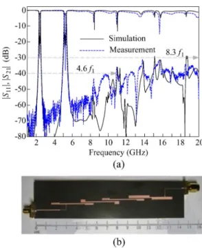
Fig. 7. (a) Simulation and measured responses of the experimental bandpass filter. (b) Photograph of the circuit.1 = 6%, 1 = 4%, ripple = 0:1 dB. L = 12 mm, s = 0:65 mm, L = 16 mm, s = 1:05 mm, L = 14:5 mm, s = 0:6 mm, d = 14:46 mm, d = 7:18 mm, ` = 22:60 mm, ` = 11:13 mm, ` = 21:85 mm, and ` = 1:13 mm. Z = 85:43 , Z = 134:05 .
IV. SIMULATION ANDMEASUREMENTRESULTS Fig. 7(a) plots the simulated and measured and re-sponses of the experimental filter designed at 2.4/5.2 GHz. The constitutive resonators are in Table I. As shown in Fig. 3(b), the spurious peaks are at 8.5, 11.5, 14, 15, 16, and 18.5 GHz. In Fig. 4, indicated by the grey dashed lines, the zero (before 20 GHz) corresponding to the first stage mm is 11.55 GHz, those to the second stage mm are 8.73 and 15.9 GHz, and those to the third stage mm are 9.54 and 16.8 GHz. The reason why these zero frequencies are slightly different from those of the spurious peaks listed above is that the three coupling lengths must fulfill the same frac-tional bandwidth at and . The zeros created by the tapped input ( , see also the grey dashed line in Fig. 6) are 3.45, 11.73, and 18.88 GHz and those by the tapped output are 8.39 and 24.5 GHz. Note that the two fractional bandwidths are different from those in Fig. 3(b) since the coupling lengths are changed, as explained in the second paragraph of Section III-A. It is noted that when either fractional bandwidth is changed, the positions of the spurious peaks remain almost unchanged since they are the higher order resonances of the resonators.
The measured response shows that the in-band return losses are 16.2 and 16.7 dB and the insertion losses are 2.49 and 2.79 dB at the design frequencies and , respectively. The upper stopband of the test filter is extended to 11 GHz and 20 GHz for rejection levels of 40 and 30 dB, respectively. The measured data agree well with the simulated responses. Fig. 7(b) is a photograph of the experimental circuit.
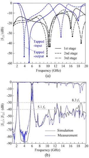
Fig. 8 plots the results of a dual-band filter designed at GHz and GHz. The geometric parameters of the resonators are listed in Table III. Fig. 8(a) shows the
re-Fig. 8. (a)jS j responses of the coupled stages and tapped input/output struc-tures. (b) Simulation and measured responses of the experimental filter.f = 2:4 GHz, f = 6:0 GHz, 1 = 5%, 1 = 4:7%, and ripple = 0:1 dB. ` = 15 mm, s = 0:57 mm, ` = 14 mm, s = 0:38 mm, ` = 12:5 mm, s = 0:2 mm, d = 7:73 mm, d = 11:33 mm, ` = 7:7 mm, ` = 9:49 mm, ` = 24:76 mm, and ` = 7:18 mm. Z = 146:36 , Z = 81:74 , Z = 79:33 , and Z = 127:99 . TABLE III
GEOMETRICDIMENSIONS OF THEFOURSTEPPED-IMPEDANCERESONATORS FORDESIGN OF THE2.4/6.0-GHz DUAL-BANDFILTER
sponses of the three stages and the tapped input/output struc-tures, after having been tuned for sliding transmission zeros to suppress the spurious passbands. In simulation, the parts of each coupled stage without coupling are directly truncated and the truncation planes are used as the termination ports with refer-ence impedances . Since only the positions of the zeros are of interest in this design, the values of the port impedance are not important. One can observe that the tap structure also con-tributes strong attenuations in the band between the two center frequencies in addition to the zeros at 13.57 and 18.08 GHz. As a final note, the theoretical lengths of the dual-band transformer
are mm, mm, mm, and
mm. Extra, but easy, fine trimming is required to
and/or shrink , and vice versa. Two or three iterations are sufficient for the tuning. The measured response shows that the in-band insertion losses are 1.85 and 2.98 dB at and , re-spectively. The upper stopband of the test filter is extended to 12.2 GHz and to 20 GHz for rejection levels of 40 and 30 dB, respectively. The measured data agree well with the simulated responses.
V. DISCUSSION
Although the circuit configuration in Fig. 1 is similar to [2, Fig. 9] and [13, Fig. 1], the entire design involves a large number of circuit variables and much effort for circuit tuning. As the results show in Fig. 3, the dual-band filters with either four identical or dissimilar resonators have poor rejection characteristics in the upper stopband. This does create the need of optimization of circuit parameters for enhancing the filter performance in the upper rejection band. It is important to note that the optimization does rely on various analytical techniques for generating transmission zeros for suppressing the spurious peaks using the nature of the structure itself, rather than on pure numerical computation.
VI. CONCLUSION
This paper has demonstrated a systematic design and tuning procedure for realizing bandpass filters with a dual-passband sponse and an extended upper rejection band with improved re-jection levels. The resonating elements are planned to have two leading resonant frequencies to fulfill the dual-band character-istic and to have staggered higher order resonances to prevent spurious peaks of high levels and wide bandwidth from the co-herent resonances. The circuit performances in the stopband are further improved by suppressing the spurious peaks with trans-mission zeros tuned by changing the coupling lengths of the coupled stages and sliding the tap positions of the dual-band transformers at the end resonators. Bandwidth and dual-band transformer design graphs are provided to clearly demonstrate the detailed synthesis data for circuit realization. The measured results of two test fourth-order circuits show that rejection levels of 30 dB can be achieved up to more than eight times the first center frequency.
ACKNOWLEDGMENT
The authors thank Dr. M. Jiang, Department of Computer and Communication Engineering, Tahwa Institute of Technology, Hsinchu, Taiwan, for his valuable comments to this study.
REFERENCES
[1] J.-T. Kuo and H.-S. Cheng, “Design of quasi-elliptic function filters with a dual-passband response,” IEEE Microw. Wireless Compon. Lett., vol. 14, no. 10, pp. 472–474, Oct. 2004.
[2] J.-T. Kuo, T.-H. Yeh, and C.-C. Yeh, “Design of microstrip bandpass filters with a dual-passband response,” IEEE Trans. Microw. Theory
[3] C.-C. Chen, “Dual-band bandpass filter using coupled resonator pairs,”
IEEE Microw. Wireless Compon. Lett., vol. 15, no. 4, pp. 259–261, Apr.
2005.
[4] C.-Y. Chen and C.-Y. Hsu, “A simple and effective method for microstrip dual-band filters design,” IEEE Microw. Wireless Compon.
Lett., vol. 16, no. 5, pp. 246–248, May 2006.
[5] X. Y. Zhang, J.-X. Chen, Q. Xue, and S.-M. Li, “Dual-band bandpass filters using stub-loaded resonators,” IEEE Microw. Wireless Compon.
Lett., vol. 17, no. 8, pp. 583–585, Aug. 2007.
[6] P. Mondal and M. K. Mandal, “Design of dual-band bandpass filters using stub-loaded open-loop resonators,” IEEE Trans. Microw. Theory
Tech., vol. 56, no. 1, pp. 150–155, Jan. 2008.
[7] X. Y. Zhang and Q. Xue, “Novel dual-mode dual-band filters using coplanar-waveguide-fed ring resonators,” IEEE Trans. Microw. Theory
Tech., vol. 55, no. 10, pp. 2183–2190, Oct. 2007.
[8] P. K. Singh, S. Basu, and Y.-H. Wang, “Miniature dual-band filter using quarter wavelength stepped impedance resonators,” IEEE
Mi-crow. Wireless Compon. Lett., vol. 18, no. 2, pp. 88–90, Feb. 2008.
[9] J.-T. Kuo, W.-H. Hsu, and W.-T. Huang, “Parallel-coupled microstrip filters with suppression of harmonic response,” IEEE Microw. Wireless
Compon. Lett., vol. 12, no. 10, pp. 383–385, Oct. 2002.
[10] J.-T. Kuo, S.-P. Chen, and M. Jiang, “Parallel-coupled microstrip filters with over-coupled end stages for suppression of spurious responses,”
IEEE Microw. Wireless Compon. Lett., vol. 13, no. 10, pp. 440–442,
Oct. 2003.
[11] M. Jiang, M.-H. Wu, and J.-T. Kuo, “Parallel-coupled microstrip fil-ters with over-coupled stages for multispurious suppression,” in IEEE
MTT-S Int. Microw. Symp. Dig., Long Beach, CA, Jun. 12–17, 2005,
pp. 687–690.
[12] T. Lopetegi, M. A. G. Laso, F. Falcone, F. Martin, J. Bonache, J. Garcia, L. Perez-Cuevas, M. Sorolla, and M. Guglielmi, “Microstrip ‘wiggly-line’ bandpass filters with multispurious rejection,” IEEE
Microw. Wireless Compon. Lett., vol. 14, no. 11, pp. 531–533, Nov.
2004.
[13] J.-T. Kuo and E. Shih, “Microstrip stepped-impedance resonator band-pass filter with an extended optimal rejection bandwidth,” IEEE Trans.
Microw. Theory Tech., vol. 51, no. 5, pp. 1554–1559, May 2003.
[14] C.-F. Chen, T.-Y. Huang, and R.-B. Wu, “Design of microstrip band-pass filters with multi-order spurious-mode suppression,” IEEE Trans.
Microw. Theory Tech., vol. 53, no. 12, pp. 3788–3793, Dec. 2005.
[15] M. Jiang, H.-P. Lin, and J.-T. Kuo, “Design of quasi-elliptic function filters with dual-passband responses and multi-spurious suppression,” in Proc. Asia–Pacific Microw. Conf., 2007, pp. 2365–2368.
[16] M. Mokhtaari, K. Rambabu, J. Bornemann, and S. Amari, “Advanced stepped-impedance dual-band filters with wide second stopbands,” in
Proc. Asia–Pacific Microw. Conf., 2007, pp. 2285–2288.
[17] C. Monzon, “A small dual-frequency transformer in two sections,”
IEEE Trans. Microw. Theory Tech., vol. 51, pp. 1157–1161, Apr. 2003.
[18] J.-T. Kuo, C.-C. Yeh, and F.-C. Hsu, “Design of vertically stacked stepped-impedance resonator (SIR) filters with a dual-passband re-sponse,” Int. J. Microw. Opt. Technol., vol. 1, no. 2, pp. 371–377, Aug. 2006.
[19] IE3D Simulator. Zeland Softw., Fremont, CA, Jan. 1997.
Jen-Tsai Kuo (S’88–M’92–SM’04) received the
Ph.D. degree from the Institute of Electronics, National Chiao Tung University (NCTU), Hsinchu, Taiwan, in 1992.
Since 1984, he has been with the Department of Communication Engineering, NCTU, where he is currently a Professor. From 1995 to 1996, he was a Visiting Scholar with the Electrical Engineering Department, University of California Los Angeles (UCLA). His research interests include analysis and design of microwave integrated circuits and numerical techniques in electromagnetics.
Dr. Kuo is currently an Editorial Board member of the IEEE TRANSACTIONS ONMICROWAVETHEORY ANDTECHNIQUESand the IEEE MICROWAVE AND
WIRELESSCOMPONENTSLETTERS. He was a recipient of the Best Paper Award presented at the 2002 National Telecommunication Conference, Taiwan, and the 2007 Asia–Pacific Microwave Conference (APMC) Prize, Bangkok, Thailand. He was also the recipient of the 2006 Taiwan Citation Laureate presented by Thomson Scientific and the 2007 Distinguished Research Award presented by the National Science Council, Taiwan.
Huei-Ping Lin received the B.S. degree in
com-munication engineering from Yuan Tze University, Taoyuan, Taiwan, in 2006, and is currently working toward the M.S. degree in communication engi-neering from National Chiao Tung University, Hsinchu, Taiwan.
Her research interests include analysis and design of passive microwave integrated circuits.