Fabrication of SONOS-Type Flash Memory with the Binary
High-k Dielectrics by the Sol-Gel Spin Coating Method
Fu-Hsiang Ko,a,*
,zHsin-Chiang You,bChun-Ming Chang,aWen-Luh Yang,c and Tan-Fu Leib
a
Institute of Nanotechnology, and bInstitute of Electronics Engineering, National Chiao Tung University, Hsinchu 300, Taiwan
c
Department of Electronic Engineering, Feng Chia University, Taichung 407, Taiwan
We fabricated the binary high-k共HfxZr1−xO2兲 nanocrystal memory using a very simple sol-gel spin coating method and 900°C 60 s
rapid thermal annealing共RTA兲. From the transmission electron microscopy identification, the nanocrystals were formed as the monolayered charge trapping site after 900°C 60 s RTA and the size was ca. 5 nm. We verified the electrical properties in terms of program-erase speed, charge retention, and endurance. The sol-gel device exhibited the long charge retention time of 104s with
only 2.5% charge loss, and good endurance performance for program/erase cycles up to 105.
© 2007 The Electrochemical Society. 关DOI: 10.1149/1.2433705兴 All rights reserved. Manuscript submitted October 5, 2006; revised manuscript received November 20, 2006. Available electronically February 5, 2007.
Conventional flash memory devices use floating gate structure and charge is stored in polysilicon floating gate.1But, when tunnel-ing oxide is below 65 nm, floattunnel-ing gate structure faces scaltunnel-ing issues.2The storage charge leaks easily due to defects in the tunnel-ing oxide formed by repeated program-erase cycles. So, discrete trap memory devices like polysilicon-oxide-nitride-silicon 共SONOS兲 structure and nanocrystal memory are widely studied to replace floating gate structure for semiconductor memory application.3-7The charge trapping layer of traditional SONOS memory is silicon ni-tride共Si3N4兲. High-k materials are considered as charge storage
ma-terial to get faster programming speed and better charge retention performance. But, SONOS high-k memory has the electron migra-tion problem in the charge trapping layer;5 this will cause charge loss and degrade the charge retention performance. The nanocrystal memory can keep the charge trapped tightly to avoid the charge loss problem of SONOS memory and also achieve the advantages like fast program-erase speed, low programming voltage, and good en-durance as SONOS memory.8,9
Recently, numerous technologies have been developed for the preparation of various high-k films. To prepare insulating thin films, atomic layer deposition 共ALD兲, physical vapor deposition 共PVD兲, and chemical vapor deposition共CVD兲 methods have all been used to prepare films for new technologies.10-12The sol-gel method is a very interesting simple technique for preparing the high-k dielectric films13or memory charge trapping films.14
The sol-gel method can provide colloidal solvents or precursor compounds when metal halides are hydrolyzed under controlled conditions in the beaker. In the sol-gel process, hydrolysis, conden-sation, and polymerization steps occur to form metal-oxide networks in the solution. The most interesting feature of sol-gel processing in the solution is its ability to synthesize new types of materials that are known as “inorganic-organic hybrids.”15Film formation with spin coating is a simpler method than ALD, PVD, or CVD to deposit the sol-gel materials due to its cheaper precursor and tool. In addition, the film can be fabricated in the normal pressure system instead of high vacuum system.16
In this paper, we used the sol-gel spin coating method to fabri-cate a SONOS-type flash memory device. We used the sol-gel method to combine two different high-k precursors, i.e., HfCl4and
ZrCl4, together to form binary high-k 共HfxZr1−xO2兲 nanocrystal memory. We performed transmission electron microscope 共TEM兲 and electrical analyses, including Id-Vg, retention, and program-erase speed measurements, to evaluate the performance of the binary 共HfxZr1−xO2兲 nanocrystals memory.
Experimental
The fabrication of sol-gel spin coating nanocrystals memory started with local oxidation of silicon共LOCOS兲 isolation process on p-type 共100兲 150 mm silicon substrate. At the beginning, a 4 nm tunneling oxide was thermally grown at 925°C by furnace. The charge trapping layer was prepared using a sol-gel spin coating method. HfCl4共99.5%, Aldrich, USA兲 and ZrCl4共99.5%, Aldrich, USA兲 were used as the precursors. Initially, we prepared a solution for which the molar ratio of HfCl4:ZrCl4:isopropanol is 1:1:1000.
The charge trapping layer was deposited by spin coating at 3000 rpm for 60 s at ambient temperature共25°C兲. The spin-coater used was TEL Clean Track model MK8共Japan兲. After spin coating, the wafer was under rapid thermal annealing共RTA兲 at 900°C for 60 s in O2 ambient to form HfxZr1−xO2 nanocrystals. The RTA temperature13 should range from 900–1050°C to meet the below source/drain共S/D兲 annealing condition. Hence, we chose 900°C due to the lower device damage and thermal budget.13,14The blocking oxide 30 nm was deposited by high density plasma chemical vapor deposition共HDPCVD兲 tetraethyl orthosilicae 共TEOS兲 followed by poly-Si gate 200 nm deposition. Finally, gate patterning, S/D im-plant, and the rest of the subsequent complementary metal oxide semiconductor共CMOS兲 processes were used to fabricate this nano-crystal memory. A self-aligned implantation was used to perform the n+S/D extension with the As+dosage of 5⫻ 1015cm−2at the
en-*Electrochemical Society Active Member. z
E-mail: [email protected] Figure 1. The process flow of the binary high-k SONOS-type memory.
Journal of The Electrochemical Society, 154共4兲 H268-H270 共2007兲 0013-4651/2007/154共4兲/H268/3/$20.00 © The Electrochemical Society H268
) unless CC License in place (see abstract).
ecsdl.org/site/terms_use
address. Redistribution subject to ECS terms of use (see
140.113.38.11
ergy of 20 keV. The channel length of the memory device was 0.35m. The process flow and the structure of the sol-gel SONOS-type memory are depicted in Fig. 1 and 2, respectively.
Results and Discussion
The high-resolution transmission electron microscopy共HRTEM兲 image in Fig. 3 depicts the nanocrystals on SiO2film after annealing
at 900°C for 60 s. The average nanocrystal size is around 5 nm. Tang et al.15have studied the detailed synthesis of HfxZr1−xO2
nano-crystals at various conditions in the solution. They suggest the molar fraction of Hf or Zr in the nanocrystal from ⬃330°C reaction is quite complex and cannot be determined. Similarly, the binary nano-crystal is formed in our SONOS-type memory after 900°C anneal-ing, and the molar fraction of Hf or Zr is still unknown due to the unavailability of analytical tools.
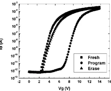
Figure 4 shows the Id-Vgcurve of the SONOS memory. We use channel hot electron injection to program, and band to band tunnel-ing induced hot hole injection to erase. The program condition is Vg= 15 V, Vd= 10 V for 10 ms. The erase condition is Vg=
−10 V, Vd= 10 V for 1 s. We can read the Vth shift 共⫽ “Vth of program” - “Vth of erase”兲 about 4 V from Fig. 4. The subthreshold slopes of Id-Vgcurves are different for the fresh cell and erased cell.
The degradation of the subthreshold swing of the device with local-ized charge trapping is attributed to a subsurface conduction under-neath the charge trapping region. Figure 5 shows the program speed
of the HfxZr1−xO2nanocrystal memory. We used channel hot
elec-tron 共CHE兲 to program, and the program conditions were 共i兲 Vg = 10 V, Vd= 10 V, 共ii兲 Vg= 12 V, Vd= 10 V, 共iii兲 Vg= 15 V,
Vd= 10 V, respectively. The Vth shift increases with increasing
ap-plied gate voltage, and the program speed can be as fast as 0.1 ms with 2.5 V memory window for program condition Vg= 15 V, Vd
= 10 V. We can see from the figure that, as the applied gate voltage increases, the Vth shift also increases. This is because the larger the gate voltage is applied, the more “hot” electrons are generated. There are more electrons able to cross the barrier height and trapped in the HfxZr1−xO2sites, so the Vth shift increases. The erase speed of
the HfxZr1−xO2nanocrystal memory is also demonstrated in Fig. 6.
We use band to band hot hole 共BTBHH兲 to erase, and the erase conditions are 共i兲 Vg= −10 V, Vd= 10 V, 共ii兲 Vg= −12 V, Vd = 10 V,共iii兲 Vg= −15 V, Vd= 10 V, respectively. The normalized
erase speed curve appears in Fig. 6, and the same explanation can be applied on the Vth shift as gate voltage becomes more negative. Using CHE to program and BTBHH to erase yields high program-erase efficiency. The charge retention characteristic of the sol-gel HfxZr1−xO2nanocrystal memory is demonstrated in Fig. 7. The nor-malized Vth shift is defined as the ratio of the Vth shift at the time of interest and at the beginning. Using this as an indicator, we can see the charge loss for the nanocrystal memory. The curve is obtained in Figure 2. The structure of the binary high-k SONOS-type memory.
Figure 3. The TEM image of the binary high-k nanocrystals.
Figure 4. Id-Vgcurve of the binary high-k SONOS-type memory.
Figure 5. The program speed of the binary high-k SONOS-type memory. H269
Journal of The Electrochemical Society, 154共4兲 H268-H270 共2007兲 H269
) unless CC License in place (see abstract).
ecsdl.org/site/terms_use
address. Redistribution subject to ECS terms of use (see
140.113.38.11
program condition of Vg= 12 V and Vd= 10 V at 10 ms under
room temperature and 85°C, respectively. The room temperature retention curve shows only 2.5% charge loss as time is measured up to 104s. The 85°C curve exhibits ⬃15% charge loss. This result
indicates the HfxZr1−xO2nanocrystals in the charge trapping site can
tightly catch the tunneling electrons. Hence, the electrons trapped by the sol-gel-derived nanocrystal devices did not easily escape, and the exhibited charge loss percentage is quite low. Figure 8 shows the endurance characteristics of the nanocrystal memory. The measure-ment condition is programmed under Vg= 15 V and Vd= 10 V for
1 ms, and is erased under Vg= −10 V and Vd= 10 V for 10 ms. As the figure shows, the memory window is about 3.6 V after 105 program/erase 共P/E兲 cycles. No significant window narrowing is observed. This observation verifies the reliability of our sol-gel-derived HfxZr1−xO2nanocrystal memory.
Conclusions
In this paper, we used a sol-gel spin coating method to form nanocrystals as the charge trapping site of SONOS memory. The TEM analysis indicates the formation of⬃5 nm HfxZr1−xO2
nano-crystals. We have verified the device performance with the P/E speed, charge retention, and endurance. The quality of the nanocrys-tals formed by the sol-gel spin coating method and RTA treatment exhibits better properties in terms of fast P/E speed, long charge retention time, and good endurance with no memory window nar-rowing.
Acknowledgments
This study was supported financially by the National Science Council, Taiwan, through contract no. NSC 95-2113-M-009-032-MY3. The memory devices were carried out using the facilities lo-cated in the National Nano Device Laboratories.
National Chiao Tung University assisted in meeting the publication costs of this article.
References
1. R. Bez, E. Camerlenghi, A. Modelli, and A. Visconti, Proc. IEEE, 91, 489共2003兲. 2. B. D. Salvo, C. Gerardi, R. V. Schaijk, S. A. Lombardo, D. Corso, C. Plantamura, T. Serafino, G. Ammendola, M. V. Duuren, P. Goarin, W. Y. Mei, K. V. D. Jeugd, H. Baron, M. Gély, P. Mur, and S. Deleonibus, IEEE Trans. Device Mater. Reliab.,
4, 377共2004兲.
3. Y.-N. Tan, W.-K. Chim, B. J. Cho, and W.-K. Choi, IEEE Trans. Electron Devices, 51, 1143共2004兲.
4. Y. N. Tan, W. K. Chim, W. K. Choi, M. S. Joo, T. H. Ng, and B. J. Cho, Tech. Dig.
- Int. Electron Devices Meet., 2004, 889.
5. T. Sugizaki, M. Kohayashi, M. Ishidao, H. Minakata, M. Yamaguchi, Y. Tamura, Y. Sugiyama, T. Nakanishi, and H. Tanaka, VLSI Tech. Symposium, 27共2003兲. 6. X. Wang, and D. L. Kwong, IEEE Trans. Electron Devices, 53, 78共2006兲. 7. M. H. White, D. A. Adams, and J. Bu, IEEE Circuits Devices Mag., 22,共2000兲. 8. M. She and T. J. King, IEEE Trans. Electron Devices, 50, 1934共2003兲. 9. M. Takata, S. Kondoh, T. Sakaguchi, H. Choi, J.-C. Shim, H. Kurino, and M.
Koyanagi, Tech. Dig. - Int. Electron Devices Meet., 2003, 553.
10. S. Kamiyama, T. Miura, and Y. Nara, J. Electrochem. Soc., 153, G187共2006兲. 11. J. Y. Tewg, Y. Kuo, and J. Lu, J. Electrochem. Soc., 152, G643共2005兲. 12. L. Goux, H. Vander Meeren, and D. J. Wouters, J. Electrochem. Soc., 153, F132
共2006兲.
13. H.-C. You, F.-H. Ko, and T.-F. Lei, J. Electrochem. Soc., 153, F94共2006兲. 14. T.-H. Hsu, H.-C. You, F.-H. Ko, and T.-F. Lei, J. Electrochem. Soc., 153, G934
共2006兲.
15. J. Tang, J. Fabbri, R. D. Robinson, Y. Zhu, I. P. Herman, M. L. Steigerwald, and L. E. Brus, Chem. Mater., 16, 1336共2004兲.
16. H.-C. You, T.-H. Hsu, F.-H. Ko, J.-W. Huang, W.-L. Yang, and T.-F. Lei, IEEE
Electron Device Lett., 27, 644共2006兲. Figure 6. The erase speed of the binary high-k SONOS-type memory.
Figure 7. Charge retention curve of the binary high-k SONOS-type memory at room temperature and 85°C, respectively.
Figure 8. The endurance characteristic of the binary high-k SONOS-type memory.
H270 Journal of The Electrochemical Society, 154共4兲 H268-H270 共2007兲
H270
) unless CC License in place (see abstract).
ecsdl.org/site/terms_use
address. Redistribution subject to ECS terms of use (see
140.113.38.11