1772 IEEE PHOTONICS TECHNOLOGY LETTERS, VOL. 23, NO. 23, DECEMBER 1, 2011
Enhanced Performance of LEDs Using Periodic
Tent-Like Post Patterns on A-plane
Sapphire Substrates
Bo-Wen Lin, Chung-Cheng Chang, Cheng-Yu Hsieh, Bau-Ming Wang, YewChung Sermon Wu, and
Wen-Ching Hsu
Abstract—Periodic tent-like post patterns on a-plane sapphire substrates were fabricated using a two-step etching process. They were denoted as a-plane dot pattern sapphire substrate (ADPSS). Compared with the GaN-based light-emitting diode (LED) grown on a-plane sapphire without any pattern (AFlat), the ADPSS-LED has higher output power, light extraction efficiency (LEE), and ex-ternal quantum efficiency (EQE), and better crystal quality. The output power of ADPSS-LED was 9.6 mW, which was 68.4% larger than the AFlat-LED. In addition, the blue shift of ADPSS-LED was found to be less than that of AFlat-LED.
Index Terms—A-plane, light-emitting diode (LED), sapphire. I. INTRODUCTION
L
IGHT-EMITTING diodes (LEDs) are expected to play an important role in next-generation light source due to their advantages of high efficiency, long life, small size, environ-mental protection, various colors and wide applications. In par-ticular, high-brightness GaN-based LEDs have attracted consid-erable attention for white light solid-state lighting. GaN-based LEDs are usually grown on c-plane sapphire substrate. The per-formance of these LEDs can be improved by using patterned c-plane sapphire substrate [1]–[3]. However, using c-plane sub-strate is waste of sapphire material. Since the growth direction of sapphire boule was usually along -axis, -axis sapphire ingot has to be drilled from the side wall of sapphire boule. As a result, only about 20% of -axis sapphire boule was used to fabricate c-plane substrates.The economical way to grow GaN-based LEDs on sap-phire substrate is using a-plane sapsap-phire. The lattice mismatch between -axis sapphire and GaN lattice is only 2% [4]. Un-fortunately, they have different arrangement of the lattices.
Manuscript received June 09, 2011; revised August 15, 2011; accepted September 01, 2011. Date of publication September 12, 2011; date of current version November 09, 2011. This work was supported by Sino American Silicon Products Incorporation and by the National Science Council of the Republic of China under Grant 98-2221-E009-041-MY3.
B.-W. Lin, C.-C. Chang, C.-Y. Hsieh, and B.-M. Wang are with the Depart-ment of Materials Science and Engineering, National Chiao Tung University, Hsinchu 30010, Taiwan.
Y. S. Wu is with the Department of Materials Science and Engi-neering, National Chiao Tung University, Hsinchu 30010, Taiwan (e-mail: [email protected]).
W.-C. Hsu is with the Sino-American Silicon Products Incorporation, Hsinchu, 300, Taiwan.
Color versions of one or more of the figures in this letter are available online at http://ieeexplore.ieee.org.
Digital Object Identifier 10.1109/LPT.2011.2167677
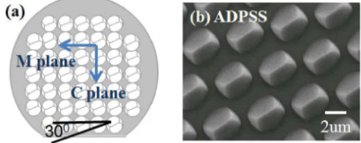
Fig. 1. Schematic illustrations and SEM image of ADPSS.
To grow GaN-based LEDs on -axis sapphire substrate is not easy. Most of previous studies were about the improvement of crystal quality, not the performance of LED.
In this study, the periodic tent-like array patterned was in-troduced to the a-plane sapphire substrate to grow GaN-based LEDs. The morphology, the crystallinity and the performance of LEDs were investigated.
II. EXPERIMENTS
The periodic dot array patterned a-plane sapphire substrate was employed to grow GaN-based LEDs. It was designated as “ADPSS” (A-plane Dot Pattern Sapphire Substrate), which was prepared by standard photolithography (3- m circle diameter and 1.5- m spacing). The photoresist pattern was used as the dry-etching mask. The dot patterns were first defined by induc-tively coupled plasma (ICP) [5]–[12], and then etched in hot H PO —based solutions [13], [14]. Fig. 1 shows the surface morphology of the tent-like post array patterns on a-plane sap-phire substrate. The height of patterns was 1.0 m. The bottom width and length of the tent was 2.8 m and 3.3 m, respec-tively. The ridgeline direction of the tent-like patterns was about
toward as shown in Fig. 1.
After the clean process, the LED structures were grown by metal–organic chemical vapor deposition (MOCVD). The structures comprised a buffer layer on the ADPSS, a undoped-GaN layer film, a n-GaN layer, a Si-doped AlGaN cladding layer, an InGaN–GaN multiple quantum well (MQW) with emission wavelength in the blue region, a Mg-doped AlGaN cladding layer and a p-GaN layer.
The device mesa with a chip size of 300 300 m 2 was then defined by ICP to remove Mg-doped GaN layer and MQW until the Si-doped GaN layer was exposed. The indium tin oxide (ITO) layer was then deposited to form a p-side contact layer and a current spreading layer. The Cr/Au layer was deposited
LIN et al.: ENHANCED PERFORMANCE OF LEDs USING PERIODIC TENT-LIKE POST PATTERNS 1773
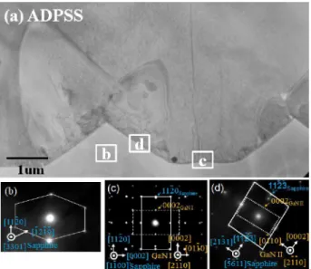
Fig. 2. Bright-field TEM images of (a) ADPSS-LED. (b), (c), and (d) are SAD patterns taken from (a) ADPSS-LED. These patterns are from (b) sapphire pat-tern, (c) interface region between GaN I and sapphire substrate, and (d) interface region between GaN II and sapphire.
onto the ITO layer to form the p-side and n-side electrodes. For the purpose of comparison, a-plane sapphire without any pat-tern was also used to grow LED structures. It was denoted as AFlat-LED (A-plane Flat LED).
III. RESULTS ANDDISCUSSION
Transmission electron-microscopy (TEM) was used to verify the natures of sapphire dot patterns and GaN crystals. Cross-sec-tional TEM image of GaN grown on ADPSS is shown in Fig. 2. To realize the orientation relationships among dot patterns and a-plane sapphire substrate, selected area diffraction (SAD) pat-terns were taken from dot patpat-terns. As shown in Fig. 2(b), the ridgeline direction of the tent-like pattern was , which was at an angle of 27.7 degrees from the direction. This angle was close to that observed in Fig. 1.
Two kinds of GaNs were found on ADPSS-LED. One (GaN I) was initiated from a-plane of ADPSS. The other (GaN II) was from sidewalls of ADPSS. To realize the crystallographic relationships among GaN and sapphire substrate, SAD patterns were taken from GaN I, GaN II and ADPSS (Fig. 2(c) and (d)). GaN I film was polar GaN layer (0001) [15], [16]. The crystallo-graphic relationship between GaN I and sapphire is established
as ,
and . This orientation
rela-tionship is usually seen in the case of a GaN epitax-ially grown on an a-plane sapphire [16]–[18]. On the other hand, the relationship between GaN II and
sap-phire is established as and
.
As for AFlat-LED, only GaN I was observed. The crystallo-graphic relationship between GaN grown film and sapphire is the same as that of GaN I epitaxially grown on an a-plane of ADPSS.
The light–current–voltage ( – – ) characteristics of the LEDs are shown in Fig. 3. The performance of ADPSS-LEDs was better than that of AFlat-LED. The light output power and
Fig. 3. – – curves of LEDs.
TABLE I
PARAMETERS ANDPERFORMANCES OFLEDs
the external quantum efficiency (EQE) of LEDs were listed in Table I. The output power of ADPSS-LED was 9.6 mW, which was 68.4% larger than the AFlat-LED at an injection current of 20 mA. The EQE of ADPSS-LED was 15.5%, which was 9.2% larger than the AFlat-LED. This indicates that light extraction efficiency (LEE) of ADPSS-LED and/or GaN crystal quality are better than those of AFlat-LED. Since the surface of ADPSS substrate was “rougher” than that of AFlat substrate, obviously the LEE of ADPSS-LED was better than that of AFlat-LED [19], [20].
The nature of GaN crystal quality was analyzed by (1) X-ray diffraction (XRD), (2) electrical luminescence (EL) and (3) screw dislocation density, which can be characterized by etching pit density (EPD). As listed in Table I, compared with AFlat-LED, the full width at half maximum (FWHM) of (002) GaN was decreased from 438.5 to 298.9 arcsec, and the FWHM of (102) GaN was decreased from 819.4 to 305.8 arcsec. EL analysis also revealed that the ADPSS-LED has a smaller FWHM value (16 nm) than that of AFlat-LED (17.9 nm). Besides, the EPD of ADPSS-LED was 0.52 cm , which was less than that of the AFlat-LED, 1.26 cm . These results all indicate the GaN structural quality of ADPSS-LED are better than that of AFlat-LED as listed in Table I.
The observed differences in crystal qualities might be due to the lateral growth of GaN. In this case, most of the growth of GaN was initiated not from sidewall surfaces but a-planes. As the growth time increased, GaN epilayers on the bottom a-plane covered these sidewall surfaces by lateral growth, which is sim-ilar to the epitaxial lateral overgrowth (ELOG) mode [16], [17]. Beside the improvement of GaN structural quality, the blue shift of ADPSS-LED was found to be less than that of AFlat-LED, as shown in Fig. 4. When the injection current of LEDs increased from 20 to 80 mA, the blue shift of the wavelength of ADPSS-LED was 0.36 nm, which was only
1774 IEEE PHOTONICS TECHNOLOGY LETTERS, VOL. 23, NO. 23, DECEMBER 1, 2011
Fig. 4. Blue shifts phenomenon of AFlat-LED and ADPSS-LED by various injections current.
4.9% of AFlat-LED (7.3 nm). In other words, compared with AFlat-LED, ADPSS-LED not only has higher brightness, but also has smaller blue shift [21], [22].
IV. CONCLUSION
Periodic dot array a-plane sapphire substrate (ADPSS) was employed to grow GaN-based LEDs. ADPSS was fabricated using two steps etching process. The shape of dot patterns was tent-like. The ridgeline direction of the tents was , which was at an angle of 27.7 degrees from the . The output power of ADPSS-LED was 9.6 mW, which was 68.4% larger than the AFlat-LED at an injection current of 20 mA. The crys-tallinity of ADPSS-LEDs was better than that of AFlat-LED. Compared with AFlat-LED, the FWHM of (002) GaN was de-creased from 438.5 to 298.9 arcsec, and the FWHM of (102) GaN was decreased from 819.4 to 305.8 arcsec. Besides, the ADPSS-LED has a smaller blue shift value than AFlat-LED. In other words, compared with AFlat-LED, ADPSS-LED not only has higher brightness, but also has smaller blue shift.
ACKNOWLEDGMENT
Technical support from the National Nano Device Labora-tory, Center for Nano Science and Technology, Nano Facility Center, and Semiconductor Laser Technology Laboratory of the National Chiao Tung University are acknowledged. The authors would like to thank H. C. Kuo for valuable discussions.
REFERENCES
[1] Y. Ee, J. Biser, W. Cao, H. Chan, R. Vinci, and N. Tansu, “Metalorganic vapor phase epitaxy of III-nitride light-emitting diodes on nano-pat-terned AGOG sapphire substrate by abbreviated growth mode,” IEEE
J. Quantum Electron., vol. 15, no. 4, pp. 1066–1072, Jul./Aug. 2009.
[2] Y. Li, S. You, M. Zhu, L. Zhao, W. Hou, T. Detchprohm, Y. Taniguchi, N. Tamura, S. Tanaka, and C. Wetzel, “Defect-reduced green GaInN/GaN light-emitting diode on nanopatterned sapphire,”
Appl. Phys. Lett., vol. 98, p. 151102, 2011.
[3] Y. Ee, X. Li, J. Biser, W. Cao, H. M. Chan, R. P. Vinci, and N. Tansu, “Abbreviated MOVPE nucleation of III-nitride light-emitting diodes on nano-patterned sapphire,” J. Crys. Growth, vol. 312, pp. 1311–1315, 2010.
[4] D. Doppalapudi, E. Iliopoulos, S. N. Basu, and T. D. Moustakas, “Epitaxial growth of gallium nitride thin films on a-plane sapphire by molecular beam epitaxy,” J. Appl. Phys., vol. 85, pp. 3582–3589, 1999.
[5] Y. Hsu, S. Chang, Y. Su, J. Sheu, C. Lee, T. Wen, L. Wu, C. Kuo, C. Chang, and S. Shei, “Lateral epitaxial patterned sapphire InGaN/GaN MQW leds,” J. Cryst. Growth, vol. 261, pp. 466–470, 2004. [6] D. Wuu, W. Wang, W. Shih, R. Horng, C. Lee, W. Lin, and J. Fang,
“Enhanced output power of near-ultraviolet InGaN–GaN LEDs grown on patterned sapphire substrates,” IEEE Photon. Technol. Lett., vol. 17, no. 2, pp. 288–290, Feb. 2005.
[7] Z. H. Feng and K. M. Lau, “Enhanced luminescence from GaN-based blue LEDs grown on grooved sapphire substrates,” IEEE Photon.
Technol. Lett., vol. 17, no. 9, pp. 1812–1814, Sep. 2005.
[8] W. Wang, D. Wuu, W. Shih, J. Fang, C. Lee, W. Lin, P. Han, R. Horng, T. Hsu, T. Huo, M. Jou, A. Lin, and Y. Yu, “Near-ultraviolet InGaN/GaN light-emitting diodes grown on patterned sapphire sub-strates,” Jpn. J. Appl. Phys., vol. 44, pp. 2512–2515, 2005.
[9] C. Shen, S. W. Chang, S. Chen, T. Ko, C. Kuo, and S. Shei, “Nitride-based high-power flip-chip LED with double-side patterned sapphire substrate,” IEEE Photon. Technol. Lett., vol. 19, no. 10, pp. 780–782, May 15, 2007.
[10] D. Kang, J. Song, B. Shim, E. Ko, D. Kim, S. Kannappan, and C. Lee, “Characteristic comparison of GaN grown on patterned sapphire substrates following growth time,” Jpn. J. Appl. Phys., vol. 46, pp. 2563–2566, 2007.
[11] R. Horng, W. Wang, S. Huang, S. Huang, S. Lin, C. Lin, and D. Wuu, “Growth and characterization of 380-nm InGaN/AlGaN LEDs grown on patterned sapphire substrates,” J. Cryst. Growth, vol. 298, pp. 219–222, 2007.
[12] J. Lee, J. Oh, S. Choi, Y. Kim, H. Cho, and J. Lee, “Enhancement of InGaN-based vertical LED with concavely patterned surface using patterned sapphire substrate,” IEEE Photon. Technol. Lett., vol. 20, no. 5, pp. 345–347, Mar. 1, 2008.
[13] F. Dwikusuma, D. Saulys, and T. Kuech, “Study on sapphire surface preparation for III-nitride heteroepitaxial growth by chemical treat-ments,” J. Electrochem. Soc., vol. 149, pp. G603–G608, 2002. [14] H. Gao, F. Yan, Y. Zhang, J. Li, Y. Zeng, and G. Wang, “Enhancement
of the light output power of InGaN/GaN light-emitting diodes grown on pyramidal patterned sapphire substrates in the micro- and nanoscale,”
J. Appl. Phys., vol. 103, p. 014314, 2008.
[15] T. Paskova, “Development and prospects of nitride materials and devices with nonpolar surfaces,” Phys. Stat. Sol. (b), vol. 245, pp. 1011–1025, 2008.
[16] N. Okada, Y. Kawashima, and K. Tadatomo, “Growth of m-GaN layers by epitaxial lateral overgrowth from sapphire sidewalls,” Phys. Status
Solidi (a), vol. 206, pp. 1164–1167, 2009.
[17] K. Okuno, Y. Saito, S. Boyama, N. Nakada, S. Nitta, R. G. Tohmon, Y. Ushida, and N. Shibata, “M-Plane GaN films grown on patterned a-plane sapphire substrates with 3-inch diameter,” Appl. Phys. Express, vol. 2, p. 031002, 2009.
[18] N. Okada, Y. Kawashima, and K. Tadatomo, “Direct growth of m-plane GaN with epitaxial lateral overgrowth from c-plane sidewall of a-plane sapphire,” Appl. Phys. Express, vol. 1, p. 111101, 2008.
[19] K. McGroddy, A. David, E. Matioli, M. Iza, S. Nakamura, S. DenBaars, J. S. Speck, C. Weisbuch, and E. L. Hu, “Directional emission control and increased light extraction in GaN photonic crystal light emitting diodes,” Appl. Phys. Lett., vol. 93, p. 103502, 2008.
[20] X. Li, R. Song, Y. Ee, P. Kumnorkaew, J. Gilchrist, and N. Tansu, “Light extraction efficiency and radiation patterns of III–nitride light-emitting diodes with colloidal microlens arrays with various aspect ra-tios,” IEEE Photonics J., vol. 3, no. 3, pp. 489–499, Jun. 2011. [21] R. Farrell, P. Hsu, D. Haeger, K. Fujito, S. Denbaars, J. Speck, and
S. Nakamura, “Low-threshold-current-density AlGaN-cladding-free m-plane InGaN/GaN laser diodes,” Appl. Phys. Lett., vol. 96, p. 231113, 2010.
[22] H. Zhao, G. Liu, J. Zhang, J. D. Poplawsky, V. Dierolf, and N. Tansu, “Approaches for high internal quantum efficiency green InGaN light-emitting diodes with large overlap quantum wells,” Opt. Express, vol. 19, no. S4, pp. A991–A1007, 2011.