2168-6734 (c) 2016 IEEE. Translations and content mining are permitted for academic research only. Personal use is also permitted, but republication/redistribution requires IEEE permission. See http://www.ieee.org/publications_standards/publications/rights/index.html for more information.
This article has been accepted for publication in a future issue of this journal, but has not been fully edited. Content may change prior to final publication. Citation information: DOI 10.1109/JEDS.2017.2669100, IEEE Journal of the Electron Devices Society
> REPLACE THIS LINE WITH YOUR PAPER IDENTIFICATION NUMBER (DOUBLE-CLICK HERE TO EDIT) < 1
Abstract—An effective passivation with high-density positive fixed charges was demonstrated on GaN MIS-HEMTs. The positive fixed charges at the interface between passivation and AlGaN surface can reduce the surface potential and expand the quantum well under Fermi level. Besides, to satisfy charge balance, the net charge density at the AlGaN surface must equal to the 2DEG carrier density.Thus, the positive fixed charges passivation can increase the 2DEG carrier density and improve the switching performance of GaN MIS-HEMTs. In this work, we demonstrated a high-density positive fixed charges (~2.71 × 10¹³ e/cm-2)
passivation using SiON for GaN MIS-HEMTs. The device with SiON passivation exhibits significant improvements in I–V characteristics and dynamic RON compared to the conventional
SiN passivated device.
Index Terms—AlGaN/GaN HEMT, passivation, accepter-like states, positive fixed charges.
I. INTRODUCTION
AN-based metal-insulator-semiconductor high electron mobility transistors (MIS-HEMTs) have demonstrated outstanding high-power performance making them suitable for power switching applications [1]. However, the existence of surface states at the AlGaN surface leads to current collapse when the GaN HEMTs operate under high-electric field. Therefore, the surface passivation becomes a very important issue for GaN power devices [2].
To eliminate the surface states at the AlGaN surface and improve interface quality, many groups have performed different passivation methods including different deposition techniques, materials, and surface treatments [3-5].
However, in the real case, despite the improved interface quality between the passivation layer and AlGaN, high-density interface states still exist at the interface between passivation layer and AlGaN due to the interruption of periodic crystal lattice [6]. The interface states between passivation layer and AlGaN can be divided into acceptor- and donor- like states. When the interface states are occupied by electrons, the potentials of acceptor- and donor- like states are negative and neutral, respectively. For GaN MIS-HEMTs, the 2DEG carrier Manuscript received, 2016. This work was sponsored by the NCTU-UCB I-RiCE program, and Ministry of Science and Technology.
S. C. Liu, Y. C. Lin, C. H. Chang, C. K. Huang, S. P. Tsai, and B. Y. Chen are with the Department of Materials Science and Engineering, National Chiao Tung University, Hsinchu 30010, Taiwan.
E. Y. Chang is with the Department of Electronics Engineering and Electronic Engineering, National Chiao Tung University, Hsinchu 30010, Taiwan (e-mail: edc@mail.nctu.edu.tw).
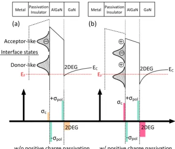
density in the access region is very sensitive to the surface potential due to the changes of the quantum well. As illustrated in Fig. 1(a), when the GaN MIS-HEMT operates under high-electric field, the electrons can be excited to fill the unoccupied acceptor-like states, leading to the AlGaN surface with a negative potential which results in the reduction of 2DEG carrier density and current collapse effect [7].
Positive fixed charges at the interface between passivation and AlGaN have been reported to be effective in reducing current collapse [7, 8]. Therefore, the passivation layer with high density of positive fixed charges is desirable to reduce the negative potential on the AlGaN surface which can improve the switching performance of GaN power devices. It was reported that SiON has higher density of positive fixed charges (Qf)
compared to pure SiN or SiO due to the increased Si+ dangling
bonds (O2N≡Si and ON2≡Si) [9, 10]. Theoretically, as
illustrated in Fig. 1(b), the positive fixed charges at the SiON/AlGaN interface can reduce the surface potential and expand the quantum well under Fermi level. Besides, to satisfy charge balance, the net charge density (σc) at the AlGaN surface,
which includes interface fixed charges, surface donor, and trapped surface charge, must equal to the 2DEG carrier density [11]. Thus, physically, the SiON passivation with high-density
Effective Passivation with High-density Positive
Fixed Charges for GaN MIS-HEMTs
Shih-Chien Liu, Chung-Kai Huang, Chia-Hua Chang, Yueh-Chin Lin, Bo-Yuan Chen, Szu-Ping Tsai,
Burhanuddin Yeop Majlis, Chang-Fu Dee, and Edward Yi Chang, Fellow, IEEE.
G
EF EC AlGaN GaN Interface states Acceptor-like Donor-like EF 2DEG 2DEGw/o positive charge passivation w/ positive charge passivation
(a) (b) EC 2DEG 2DEG σc σc +σpol +σpol -σpol -σpol Passivation Insulator
Metal Metal PassivationInsulator AlGaN GaN
Fig. 1. Schematic of band diagram and charge distribution illustrating the behaviors of charged interface states in the GaN MIS-HEMT structure under high-electric field.
2168-6734 (c) 2016 IEEE. Translations and content mining are permitted for academic research only. Personal use is also permitted, but republication/redistribution requires IEEE permission. See http://www.ieee.org/publications_standards/publications/rights/index.html for more information.
This article has been accepted for publication in a future issue of this journal, but has not been fully edited. Content may change prior to final publication. Citation information: DOI 10.1109/JEDS.2017.2669100, IEEE Journal of the Electron Devices Society
> REPLACE THIS LINE WITH YOUR PAPER IDENTIFICATION NUMBER (DOUBLE-CLICK HERE TO EDIT) < 2
positive fixed charges can effectively increase the 2DEG carrier density and improve the switching performance for GaN MIS-HEMTs.
In this work, the mechanisms of positive fixed charge passivation on GaN MIS-HEMTs were investigated in details. The results indicate that the density of positive fixed charges significantly affect the performances of GaN MIS-HEMTs.
II. DEVICE FABRICATION
The AlGaN/GaN HEMT heterostructure was grown by metal-organic chemical vapor deposition (MOCVD) on silicon substrate. The epitaxial structure consisted of 1-nm GaN cap layer, 25-nm Al0.2Ga0.8N barrier layer, 1.3-μm i-GaN layer and a
buffer layer consisted of GaN/AlGaN/AlN with total thickness of 4-μm. The device fabrication process features Ti/Al/Ni/Au ohmic contact metal and Ni/Au gate metal. The wafer was separated into two samples after mesa etch and ohmic contact formation to ensure the same starting characteristics for the devices. The gate-to-drain spacing LGD, gate-to-source spacing
LGS, and gate length LG were 10-μm, 3-μm, and 2-μm,
respectively. Both SiON and SiN films were adopted as the passivation and gate insulator for GaN MIS-HEMTs. Before ohmic metal and passivation deposition, 1-nm GaN cap layer was removed by wet etching. The schematic cross section of the AlGaN/GaN HEMT with passivation and gate insulator is shown in Fig. 2. The passivation layers were prepared by plasma-enhanced chemical vapor deposition system at 300°C and with a post deposition annealing at 500°C. The silane (2% SiH4/N2) was kept constant at 40 sccm and the flow ratios of
NH3:N2O were 1:5 and 1:0 for SiON and SiN, respectively. The
refractive index of SiON and SiN were ~1.75 and ~1.96, respectively. The SiON with refractive index of ~1.75 was optimized to form highest density of positive fixed charges. The ID,max of passivated devices versus passivation thickness are
shown in Fig. 3(a). Saturated ID,max are observed when the
passivation thicknesses are about 12 nm. III. RESULTS AND DISCUSSION
To obtain the high quality interface with different passivation materials, the N-passivation (nitridation) technique was adopted prior to SiON and SiN passivation [3, 5]. After passivation, the capacitance–voltage curves were measured with various frequencies from 1 to 500 kHz. As shown in Fig. 3(b), with N-passivation technique, the capacitance–voltage curves of SiON/AlGaN/GaN and SiN/AlGaN/GaN MIS capacitors exhibit a steep slope without hysteresis and dispersion, indicating the similar interface quality with low interface trap density using N-passivation (nitridation) technique.
The correlation of the ΔVth and the interface fixed charges
have been reported [12], which can be expressed by
∆ MIS HEMT HEMT
where, Qf is the interface fixed charge at the interface
between passivation layer and AlGaN and Cox is the capacitance
of the SiON and SiN.
For the transfer characteristics shown in Fig. 4, a large ΔVth
which was observed for the device with SiON gate insulator, indicating the existence of high-density positive fixed charges at the SiON/AlGaN interface. The Cox value of SiON and SiN
0 10 20 30 40 50 400 500 600 700 800 900 1000 1100 SiON SiN ID,m ax (m A /m m ) Passivation thickness (nm) (a) -16 -12 -8 -4 0 0 1p 2p 3p 4p 5p SiN Ca pa ci ta nc e (F ) Voltage (V) 1 k 100 k 500 k SiON (b)
Fig. 3. (a) The ID,max of passivated devices versus passivation thickness. (b) Capacitance–voltage characteristics of SiON/AlGaN/GaN and SiN/AlGaN/GaN MIS capacitors.
0 5 10 15 0 200 400 600 800 1000 1200 -12 -8 -4 010-7 10-6 10-5 10-4 10-3 10-2 10-1 100 101 102 103 104 SiON SiN w/o I D (m A/ m m ) VDS (V) 1 A/mm VGS = 0 V VDS = 10 V 73 mV/dec VGS (V) 68 mV/dec
Fig. 4. ID–VDS characteristics (left) and transfer characteristics (right) of the GaN devices with different passivation and gate insulator layers.
0 200 400 600 800 10-9 10-8 10-7 10-6 10-5 10-4 10-3 10-2 O FF -s ta te le ak ag e (A /m m ) VDS (V) SiON SiN 1 mA/mm 1 A/mm @ 750 V (a) -100 -50 0 10-12 10-11 10-10 10-9 10-8 10-7 10-6 10-5 10-4 0 5 10 15 IGS (A ) VGS (V) SiON SiN (b)
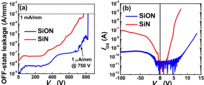
Fig. 5. (a) OFF-state drain leakage currents and (b) gate leakage currents of the GaN devices with different passivation and gate insulator layers.
Fig. 2. (a) Schematic cross section of the GaN MIS-HEMT with 12-nm passivation and gate insulator.
2168-6734 (c) 2016 IEEE. Translations and content mining are permitted for academic research only. Personal use is also permitted, but republication/redistribution requires IEEE permission. See http://www.ieee.org/publications_standards/publications/rights/index.html for more information.
This article has been accepted for publication in a future issue of this journal, but has not been fully edited. Content may change prior to final publication. Citation information: DOI 10.1109/JEDS.2017.2669100, IEEE Journal of the Electron Devices Society
> REPLACE THIS LINE WITH YOUR PAPER IDENTIFICATION NUMBER (DOUBLE-CLICK HERE TO EDIT) < 3
were calculated to be 8.7 × 10¹² F and 11.8 × 10¹² F,
respectively. The density of positive fixed charges, extracted from the formula, were ~2.71 × 10¹³ and ~1.54 × 10¹³ e/cm-2 for
SiON and SiN, respectively.
The basic DC I‒V characteristics of the devices are shown in Fig. 4. For the device with SiON passivation, a higher ID,max of
>1 A/mm, lower specific RON of 0.94 mΩ‧cm2, and lower
subthreshold slope (SS) of 68 mV/dec were observed. In contrast, the device with SiN passivation exhibits a lower ID,max
of 896 mA/mm, higher specific RON of 0.99 mΩ‧cm2, and SS of
73 mV/dec. These results reveal that the device passivated with the higher density of positive fixed charges has a higher 2DEG carrier density which is consistent with the physical phenomena as illustrated in Fig. 1.
The leakage current characteristics of the devices are shown in Fig. 5. The OFF-state breakdown characteristics, shown in Fig. 5(a), exhibit an improved BV for the device with SiON compared to the device with SiN. For the device with SiON, the BV of 750 V at a low leakage current of 1 μA/mm was achieved, yielding a high-power figure of merit of ~620 MW/cm2.
Furthermore, the device with SiON exhibits a lower gate leakage current compared to the device with SiN, as shown in Fig. 5(b). The results indicate that SiON with higher bandgap and dielectric strength effectively suppresses leakage current compared to pure SiN [13].
The dynamic RON has been commonly used to examine the
trapping effects caused by the interface states in the GaN device structure [14]. Thus, the dynamic RON can be used to evaluate
the effectiveness of the passivation. As shown in Fig. 6, the dynamic RON were extracted from various OFF-state drain
quiescent voltage (VDSQ) from 0 V to 200 V within 5 ms and
ON-state with VGS = 0 V, VDS = 1 V. The ON-state pulse width
was 50 μs using Agilent B1505A with N1267A fast switch module. For the VDSQ stress at 200 V, the dynamic RON increases
slightly to 1.2 times for the device with SiON passivation. In contrast, the dynamic RON increases 3.38 times for the device
with SiN passivation. As illustrated in Fig. 1, the increase of dynamic RON can be understood as that the quantum well was
raised by the negative potential attributed to the negatively charged acceptor-like interface states, resulting in a reduction of 2DEG carrier density [2, 7]. The results indicate that the
quantum well of SiON passivated device is more stable than the SiN passivated device under high-voltage switching. It proves that the negative potential at AlGaN surface is effectively reduced by SiON passivation with high-density positive fixed charges. The SiON passivation is therefore preferable for GaN power device applications.
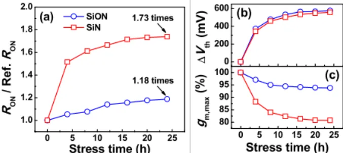
The stability of the GaN MIS-HEMT with SiON is also investigated in this study. The OFF-state (VDS = 100 V) stress
conditions were adopted to observe the stability of the devices under high-electric field [15]. The changes of RON, Vth, and
gm,max during stress for the SiON and SiN passivated devices are
shown in Fig. 7. The SiON passivated device exhibits a slight degradation in RON and gm,max after 24 hours stress. In contrast, a
severe degradation in RON and gm,max were observed for the SiN
passivated devices after 24 hours stress. For both SiON and SiN passivated devices, a ΔVth of ~560 mV were observed. Both
SiON and SiN passivated devices show saturated I-V characteristics after 20 hours stress. The results indicate that SiON passivation with higher density of positive fixed charges can improve the stability of GaN MIS-HEMTs under high-electric field.
IV. CONCLUSION
The high-density positive fixed charges passivation is proved to be effective in improving switching performance and increasing 2DEG carrier density for GaN MIS-HEMTs. The device with SiON passivation, which has higher-density positive fixed charges than SiN passivation, demonstrates significant improvements in I‒V characteristics and dynamic RON compared to the conventional SiN passivated device.
Overall, the high-density positive fixed charges passivation is desirable for GaN power device applications.
REFERENCES
[1] K.-Y. Roy. Wong, M.-H. Kwan, F.-W. Yao, M.-W. Tsai, Y.-S. Lin, Y.-C. Chang, P.-C. Chen, R.-Y. Su, J.-L. Yu, F.-J. Yang, G. P. Lansbergen, C.-W. Hsiung, Y.-A. Lai, K.-L. Chiu, C.F. Chen, M.-C. Lin, H.-Y. Wu, C.-H. Chiang, S.-D. Liu, H. -C. Chiu, P.-C. Liu, C.-M. Chen, C.-Y. Yu, C.-S. Tsai, C.-B. Wu, B. Lin, M.-H. Chang, J.-S. You, S.-P. Wang, L.-C. Chen, Y.-Y. Liao, L.Y. Tsai, Tom Tsai, H.C. Tuan & Alex Kalnitsky, "A Next Generation CMOS-Compatible GaN-on-Si Transistors for High Efficiency Energy Systems," IEEE IEDM, pp. 229-232, 2015.
[2] R. Vetury, N. Q. Zhang, S. Keller, and U. K. Mishra, "The impact of surface states on the DC and RF characteristics of AlGaN/GaN HFETs," IEEE Trans. Electron Devices, vol. 48, no. 3, pp. 560-566, Mar. 2001. [3] S. Yang, Z. Tang, K.-Y. Wong, Y.-S. Lin, C. Liu, Y. Lu, S. Huang, and K. J.
0 50 100 150 200 1.0 1.5 2.0 2.5 3.0 3.5 3.38 times D yna m ic
R
ON /S ta ticR
ONDrain quiescent bias (V) SiON
SiN
1.2 times ON-state: VGS = 0 V, VDS = 1 V Pulse width = 50 s
Fig. 6. Dynamic RON / static RON extracted from various OFF-state quiescent bias. 0 5 10 15 20 25 1.0 1.2 1.4 1.6 1.8 2.0 1.18 times SiON SiN RON / Re f. RON Stress time (h) (a) 1.73 times 0 200 400 600 0 5 10 15 20 25 80 85 90 95 100 (b) Vth (m V) (c) gm,m ax (% ) Stress time (h)
Fig. 7. Time evolutions of (a) RON, (b) ΔVth, and (c) gm,max during OFF-state stress on the GaN MIS-HEMT with SiN and SiON passivation.
2168-6734 (c) 2016 IEEE. Translations and content mining are permitted for academic research only. Personal use is also permitted, but republication/redistribution requires IEEE permission. See http://www.ieee.org/publications_standards/publications/rights/index.html for more information.
This article has been accepted for publication in a future issue of this journal, but has not been fully edited. Content may change prior to final publication. Citation information: DOI 10.1109/JEDS.2017.2669100, IEEE Journal of the Electron Devices Society
> REPLACE THIS LINE WITH YOUR PAPER IDENTIFICATION NUMBER (DOUBLE-CLICK HERE TO EDIT) < 4
Chen, "High-Quality Interface in MIS Structures With In Situ Pre-Gate Plasma Nitridation," IEEE Electron Device Lett., vol. 34, no. 12, pp. 1497-1499, Dec. 2013.
[4] S. Huang, Q. Jiang, S. Yang, C. Zhou, and K. J. Chen, "Effective passivation of AlGaN/GaN HEMTs by ALD-grown AlN thin film," IEEE Electron Device Lett., vol. 33, no. 4, pp. 516-518, Apr. 2012.
[5] S.-C. Liu, B.-Y. Chen, Y.-C. Lin, T.-E. Hsieh, H.-C. Wang, and E. Y. Chang, "GaN MIS-HEMTs With Nitrogen Passivation for Power Device Applications," IEEE Electron Device Lett., vol. 35, no. 10, pp. 1001-1003, Oct. 2014.
[6] H. Lüth, Solid surfaces, interfaces and thin films vol. 4: Springer, 2001. [7] G. Koley, V. Tilak, L. F. Eastman, and M. G. Spencer, "Slow Transients
Observed in AlGaN/GaN HFETs: Effects of SiNx Passivation and UV Illumination," IEEE Transactions Electron Device Lett., vol. 50, no. 4, pp. 886-893, Apr. 2003.
[8] Y. S. Lin, K. Y. Wong, G. P. Lansbergen, J. L. Yu, C. J. Yu, C. W. Hsiung, H. C. Chiu, S. D. Liu, P. C. Chen, F. W. Yao, R. Y. Su, C. Y. Chou, C. Y. Tsai, F. J. Yang, C. L. Tsai, C. S. Tsai, X. Chen, H. C. Tuan and Alex Kalnitsky, "Improved Trap-Related Characteristics on SiNx/AlGaN/GaN MISHEMTs With Surface Treatment," Proceedings of the 26th International Symposium on Power Semiconductor Devices & IC's, Jun., 2014.
[9] Z. Zhuo, Y. Sannomiya, Y. Kanetani, T. Yamada, H. Ohmi, H. Kakiuchi, and K. Yasutake, "Interface properties of SiOxNy layer on Si prepared by atmospheric-pressure plasma oxidation-nitridation," Nanoscale research letters, vol. 8, pp. 1-6, Dec. 2013.
[10] A. G. Aberle, "Overview on SiN surface passivation of crystalline silicon solar cells," Solar Energy materials and solar cells, vol. 65, pp. 239-248, Jan. 2001.
[11] J. P. Ibbetson, P. T. Fini, K. D. Ness, S. P. DenBaars, J. S. Speck, and U. K. Mishra, "Polarization effects, surface states, and the source of electrons in AlGaN/GaN heterostructure field effect transistors," Applied Physics Lett., vol. 77, no. 2, pp. 250-252, Nov. 2000.
[12] G. Dutta, S. Turuvekere, N. Karumuri, N. DasGupta, and A. Dasgupta, "Positive shift in threshold voltage for reactive-ion-sputtered Al 2 O 3/ AlInN/GaN MIS-HEMT," IEEE Electron Device Lett., vol. 35, no. 11, pp. 1085-1087, Nov. 2014.
[13] V. Nguyen, W. Lanford, and A. Rieger, "Variation of Hydrogen Bonding, Depth Profiles, and Spin Density in Plasma‐ Deposited Silicon Nitride and Oxynitride Film with Deposition Mechanism," Journal of The Electrochemical Society, vol. 133, pp. 970-974, May 1986.
[14] D. Jin and J. A. Del Alamo, "Methodology for the study of dynamic ON-resistance in high-voltage GaN field-effect transistors," IEEE Trans. Electron Devices, vol. 60, no. 10, pp. 3190-3196, Oct. 2013.
[15] G. Meneghesso, G. Verzellesi, F. Danesin, F. Rampazzo, F. Zanon, A. Tazzoli, M. Meneghini, and E. Zanoni, "Stability of GaN high-electron-mobility transistors: state of the art and perspectives," IEEE Trans. on Device and Materials Stability, vol. 8, no. 2, pp. 332-343, Jun. 2008.