Electromigration in Pb-free Sn Ag 3.8 Cu 0.7 solder stripes
Ying-Chao Hsu, Chung-Kwuang Chou, P. C. Liu, Chih Chen, D. J. Yao, T. Chou, and K. N. Tu
Citation: Journal of Applied Physics 98, 033523 (2005); doi: 10.1063/1.1999836 View online: http://dx.doi.org/10.1063/1.1999836
View Table of Contents: http://scitation.aip.org/content/aip/journal/jap/98/3?ver=pdfcov Published by the AIP Publishing
Articles you may be interested in
Electromigration and critical product in eutectic SnPb solder lines at 100 ° C J. Appl. Phys. 100, 024909 (2006); 10.1063/1.2216487
Ternary bulk metallic glasses formed by minor alloying of Cu 8 Zr 5 icosahedron Appl. Phys. Lett. 88, 101907 (2006); 10.1063/1.2183367
Current crowding-induced electromigration in Sn Ag 3.0 Cu 0.5 microbumps Appl. Phys. Lett. 88, 072102 (2006); 10.1063/1.2173710
Electromigration failure mechanisms for SnAg 3.5 solder bumps on Ti Cr - Cu Cu and Ni ( P ) Au metallization pads
J. Appl. Phys. 96, 4518 (2004); 10.1063/1.1788837
Electromigration of eutectic SnPb and SnAg 3.8 Cu 0.7 flip chip solder bumps and under-bump metallization J. Appl. Phys. 90, 4502 (2001); 10.1063/1.1400096
Los Angeles, California 90095
共Received 22 February 2005; accepted 16 June 2005; published online 9 August 2005兲
Electromigration behavior in the eutectic SnAg3.8Cu0.7solder stripes was investigated in the vicinity of the device operation temperature of 100 ° C by using the edge displacement technique. Measurements were made for relevant parameters for electromigration of the solder, such as drift velocity, threshold current density, activation energy, as well as the product of diffusivity and effective charge number 共DZ*兲. The threshold current densities were estimated to be 4.3 ⫻104A / cm2at 80 ° C, 3.2⫻104A / cm2at 100 ° C, and 1.4⫻104A / cm2at 120 ° C. These values represent the maximum current densities that the SnAg3.8Cu0.7 solder can carry without electromigration damage at the three stressing temperatures. The electromigration activation energy was determined to be 0.45 eV in the temperature range of 80– 120 ° C. The measured products of diffusivity and the effective charge number, DZ*, were −1.8⫻10−10cm2/ s at 80 ° C, −5.0 ⫻10−10cm2/ s at 100 ° C, and −7.2⫻10−10cm2/ s at 120 ° C. © 2005 American Institute of Physics. 关DOI: 10.1063/1.1999836兴
I. INTRODUCTION
Flip-chip technology is widely used in advanced elec-tronic products because of its higher packaging density, bet-ter performance, smaller device footprints, and lower pack-aging profiles.1 The design rule of packaging requires that each flip-chip solder bump will carry 0.2– 0.4 A, and the size of these solder bumps is already quite small, with a diameter of about 100m or less. The average current density in a bump approaches 104A / cm2. To meet the future perfor-mance requirements, even in handheld consumer products, the applied current density will increase. With the trend of miniaturization, electromigration in solder joints has been recognized as an important reliability issue for flip-chip technology.2,3
With increasing environmental concerns, the application of Pb-free solders to consumer electronic products has be-come a market driving force.4,5 The Congress of the Euro-pean Union has a directive to ban the use of Pb-based solder on July 1, 2006. Among the Pb-free solders, eutectic SnAg3.8Cu0.7solder appears to be the most promising candi-date for replacing the eutectic SnPb solder. Indeed, the Na-tional Electronics Manufacturing Initiative共NEMI兲 has rec-ommended replacing the eutectic SnPb alloy with the eutectic SnAgCu alloy in reflow processing.6 In the initial
period of mass production of Pb-free components, reliability issues such as electromigration in the SnAgCu solder are of urgent concern.
Several studies have addressed the electromigration is-sue of SnAgCu alloy.7–12Choi et al. measured the mean time to failure 共MTTF兲 of eutectic SnAgCu bumps, and they at-tempted to determine the effective charge number共Z*兲 of the solder by marker movement.7But the marker movement was too small to be measured. Lin et al. investigated the current carrying capability of eutectic SnAgCu bumps, and found that there was no electromigration damage in the bumps after stressing by 2.5⫻104A / cm2at 150 ° C for 2338 h.12 How-ever, the relevant parameters of electromigration, such as threshold current density 共Jc兲, drift velocity, activation
en-ergy 共Ea兲, and the product of diffusivity and the effective
charge number共DZ*兲 of the eutectic SnAgCu solder are still unknown.
This lack of information is because of the difficulty in preparing Blech-type electromigration test specimens of SnAgCu solder. Blech developed a unique set of test struc-tures of short stripes of Al on a TiN base line for the measurement of the drift velocity of electromigration so that the relevant parameters of electromigration can be determined.13,14 However, eutectic SnAgCu solder stripes have not been deposited by evaporation, sputtering, or elec-troplating. In addition, the solder is very soft, and it is hard to pattern it into short stripes. In this study, we report a process to fabricate solders Blech specimens, and we employed
a兲Author to whom correspondence should be addressed; electronic mail:
0021-8979/2005/98共3兲/033523/6/$22.50 98, 033523-1 © 2005 American Institute of Physics
atomic force microscopy 共AFM兲 to measure the depletion volume and drift velocity on the cathode side. As a result, we obtained a direct and precise measurement of the solder elec-tromigration parameters.
II. EXPERIMENT
A similar process to fabricate Blech’s specimens of Al stripe is adopted to fabricate the solder specimens. The main difference here is that the solder Blech specimen was fabri-cated in a Si trench, in which the top Si surface served as a polishing stopper during the subsequent polishing process. A 4-in. p-type Si wafer was cleaned by piranha solution共H2O2 and H2SO4 at the ratio of 1:7兲 for 10 min at 100 °C. After cleaning, the silicon wafer was patterned by photolithogra-phy and deep reactive ion etching共DRIE兲 to form dumbbell-shaped trenches of 3.1m in depth. Then, a 1200-Å SiO2 insulating layer was grown on the wafer. Subsequently, tita-nium and copper films with thicknesses of 1700 and 4000 Å, respectively, were thermally evaporated onto the silicon wa-fer by an e-beam evaporator. Thereafter, the copper film in-side the trench was patterned and selectively etched to form a short stripe, and two pads were also patterned on the Ti film, which served as a wetting metallization layer for the SnAgCu solder during the subsequent reflow process. Then the wafer was cut into small pieces, with a die in each piece. Solder paste of SnAg3.8Cu0.7was applied to the Cu stripe at 230 ° C for 2 s, in which the subscripts in SnAg3.8Cu0.7stand for wt %. After the reflow process, the thickness of the solder may be over 10m thick, and its shape was bumplike. Therefore, a polishing procedure was needed to thin down the solder stripe. The thickness of the solder stripe was con-trolled by the thickness of the Si trench, since the top Si surface served as a polishing stop for the solder stripe.
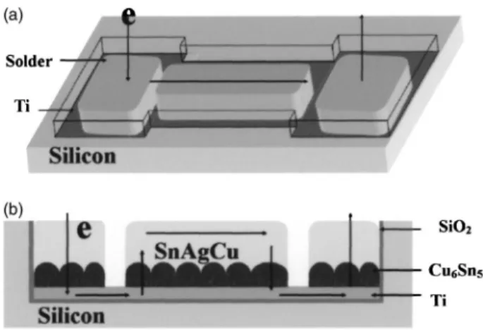
Figures 1共a兲 and 1共b兲 illustrate the schematic diagrams of the tilted and cross-sectional views of the specimen, re-spectively. The two square pads at the two sides of the speci-men were the electrodes, and the central solder stripe was the specimen to be studied. The stripe was 350m long and 80m wide. A layer of Cu6Sn5 intermetallic compound 共IMC兲 grew between the Cu and the solder during the reflow, as shown in Fig. 1共b兲. The thickness of the solder was about
1 – 2m, and it varied from sample to sample due to the polishing process, which polished some of the Si stopper. The samples were then stressed at various current densities and temperatures, and the direction of the electron flow is indicated by the arrows in Figs. 1共a兲 and 1共b兲.
Transmission electron microscopy 共TEM兲 and scanning electron microscopy 共SEM兲 were employed to observe the microstructure of the solder stripes. Focused ion beam共FIB兲 was utilized to prepare cross-sectional TEM specimens. AFM was used to measure the depletion volume on the cath-ode side of the samples. Each specimen was scanned in AFM six times in order to measure the volume before and after the current stressing; the standard deviation was less than 1% compared with the average volume. The temperature incre-ment due to the Joule heating effect was monitored by an infrared microscope, which has 0.1 ° C temperature resolu-tion and 2-m spatial resolution.
III. RESULTS
A. Microstructure of the SnAgCu stripe and temperature measurement
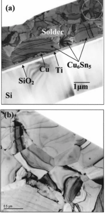
Figure 2 demonstrates the backscattered electron共BSE兲 SEM image of the fabricated solder stripe, formed inside the Si trench. Typically, the four corners of the Cu stripe could not be wetted by molten solder paste during sample prepara-tion. Figure 3共a兲 illustrates the cross-sectional TEM image of the specimen. A layer of scalloped Cu6Sn5 IMC is formed between the SnAg3.8Cu0.7solder and the Cu layer. The SiO2 and Ti layers can be clearly seen in the figure. The Cu film was consumed almost completely, but a few small Cu islands may be observed under some large IMCs. Since the Cu layer is not continuous, it is not considered when calculating the effective current density in the solder stripe. Figure 3共b兲 dis-plays the enlarged cross-sectional TEM image of the area within the white circle in Fig. 3共a兲. The grain size was about 1 m in diameter. We speculate that the minuscule grain size was due to the film thickness and the rapid cooling rate in the sample preparation process. Through theoretical calculations, it was found that about 80% of the applied current would flow inside the solder, whereas about 19% of the current drifted along the IMC layer, and only about 1% stayed in the Ti layer.
Figure 4 displays the measured temperature increment in the solder stripe as a function of current density at 80, 100, FIG. 1. 共a兲 Tilted-view schematic of the solder stripe on a Ti film in a Si
trench. 共b兲 Cross-sectional schematic of the solder Blech specimen. The direction of the electron flow is indicated by the arrows.
FIG. 2. BSE SEM image of the fabricated dumbbell-shaped stripe.
033523-2 Hsu et al. J. Appl. Phys. 98, 033523共2005兲
and 120 ° C. The highest temperature increment was merely 5 ° C when the specimen was stressed by 0.12 A, which cor-responded approximately to 1⫻105A / cm2 in the solder stripes. The Joule heating effect in the stripes was much lower than that in the flip-chip solder bump.15 This effect may be attributed to the stripe geometry and the excellent heat conduction of silicon substrate.
B. Threshold current density of the SnAg3.8Cu0.7 solder
Figures 5共a兲 and 5共b兲 show the SEM images of the SnAg3.8Cu0.7solder stripe in the cathode end before and after the current stressing by 8.67⫻104A / cm2at 80 ° C for 65 h,
respectively. After the current stressing, the SnAg3.8Cu0.7 sol-der near the cathode was depleted by the electron flow, and the intermetallic compound at the cathode side was exposed, as shown in Fig. 5共b兲. Figures 5共c兲 and 5共d兲 show the corre-sponding three-dimensional共3D兲 AFM images for the solder stripes in Figs. 5共a兲 and 5共b兲, respectively. The AFM image in Fig. 5共d兲 also shows the depletion of the cathode end, which demonstrates that the AFM could measure the deple-tion of the solder. The depledeple-tion volume for this specimen was estimated to be 799m3. On the other hand, hillocks were formed at the anode end of the stripe, as shown in Fig. 6. The composition of hillock is mainly Sn.
The average drift velocity of the solder stripe can be obtained by dividing the depletion volume共⌬V兲 by the prod-uct of the average cross-sectional area and the stressing time. Figure 7 displays the average drift velocity as a function of applied current density, showing a linear relationship for the three temperatures. By extrapolating the fitting line to the zero drift velocity, the threshold current density can be ob-tained. The estimated values are 4.3⫻104 A / cm2 at 80 ° C,
FIG. 3. 共a兲 Cross-sectional TEM image of the solder Blech specimen. 共b兲 Enlarged image of the white rectangular district in共a兲, with an average grain size of about 1m.
FIG. 4. Measured temperature increment inside the solder stripe as a func-tion of applied current for the three stressing temperatures.
FIG. 5. 共a兲 Tilted SEM image at the cathode side before current stressing. 共b兲 Tilted SEM image on the cathode side after current stressing by 8.67 ⫻104A / cm2at 80 ° C for 65 h. The SnAg
3.8Cu0.7solder was migrated by
the electron flow, but the IMC remained intact. 共c兲 Corresponding AFM image of共a兲. 共d兲 Corresponding AFM image of 共b兲.
3.2⫻104A / cm2at 100 ° C, and 1.4⫻104A / cm2at 120 ° C. These values represent the maximum current densities that the SnAg3.8Cu0.7 solder can carry without electromigration damage at the three stressing temperatures.
C. Activation energy and effective charge number of SnAg3.8Cu0.7solder
The average drift velocity due to electromigration, as given by Huntigton and Grone,16is
= J C= BeZ *j =
冉
D0 kT冊
eZ *j exp冉
− Ea kT冊
, 共1兲where J is the atom flux, C is the density of metal ions, B is the mobility, k is Boltzmann’s constant, T is the absolute temperature, eZ* is the effective charge of the ions, is the metal resistivity, j is the electrical current density, Ea is the
activation energy of diffusion, and D0 is the prefactor of diffusion constant.
Equation共1兲 can be rewritten as
vT j = D0eZ* k exp
冉
− Ea kT冊
. 共2兲Taking the logarithm of both sides of Eq.共2兲, lnvT j = −
冉
Ea kT冊
+ ln D0eZ* k . 共3兲Therefore, by measuring the solder drift velocity as a func-tion of reciprocal temperature, the activafunc-tion energy Ea and
the product of diffusivity and effective charge number, DZ*, can be obtained.
Figure 8 shows the plot of ln共vT/ j兲 as a function of the reciprocal temperature. The activation energy 共Ea兲 can be
determined from the slope of the fitted line, and its value is 0.41 eV in the temperature range of 80– 120 ° C. However, the temperature in the solder needs to be calibrated due to the Joule heating effect, as shown in Fig. 4. The real tempera-tures in the solder were higher than the ambient ones, and the activation energy was calculated to be 0.45 eV using the real temperatures.
In addition, the product of diffusion diffusivity and ef-fective charge number, DZ*, can be calculated from Eq.共3兲. Table I summarizes the product of the diffusivity and effec-tive charge number, DZ*, and its average values are −1.8 ⫻10−10cm2/ s at 80 ° C, −5.0⫻10−10cm2/ s at 100 ° C, and −7.2⫻10−10cm2/ s at 120 ° C. In order to estimate the value of Z*, the diffusivity data for pure Sn were adopted.17 The FIG. 6. Plan-view BSE SEM image of the anode side共a兲 before the current
stressing, and共b兲 after the current stressing at 80 °C for 65 h. Hillocks are composed of almost pure Sn formed at the anode side.
FIG. 7. Average drift velocity of the solder stripe as a function of applied current density. The threshold current densities were obtained by extrapolat-ing the fitted lines to zero drift velocity.
FIG. 8. Plot of the lnvT / j as a function of reciprocal temperature. The
activation energy of 0.41 eV was obtained from the slope of the fitted line.
033523-4 Hsu et al. J. Appl. Phys. 98, 033523共2005兲
average values of Z*were −27 at 80 ° C, −33 at 100 ° C, and −23 at 120 ° C, which are reasonable for solder materials.
IV. DISCUSSION
A. Threshold current density of SnAg3.8Cu0.7solder stripes
To verify if these extrapolated values of threshold cur-rent density are correct or not, some specimens were stressed at current densities below the threshold current density. Specimens were stressed at the current density of 3.5 ⫻104A / cm2 at 80 ° C, 2.6⫻104A / cm2 at 100 ° C, and 1 ⫻104A / cm2at 100 ° C for 72 h, and no detectable volume change was found.
Various stressing conditions have been investigated to study the electromigration behavior of SnAgCu bumps, and a large variety of conditions was reported to have caused dam-age in the bumps. Wu et al. conducted a MTTF experiment for SnAg4.0Cu0.5bumps with thin-film underbump metalliza-tion共UBM兲 of Al/Ni共V兲/Cu, and found that the MTTF was 1454 h for the bumps stressed by 5.0⫻103A / cm2 at 153 ° C.11 In addition, Choi et al. reported that the eutectic SnAgCu bumps with Al/ Ni共V兲/Cu UBM failed after the cur-rent stressing at 2.25⫻104A / cm2 at 140 ° C for 132 h.7 However, Lin et al. investigated the current carrying capa-bility of eutectic SnAgCu bumps with 6-m Ni underbump metallization, and found that there was no obvious electromi-gration damage in the bumps after the stressing by 2.55 ⫻104A / cm2at 150 ° C for 2338 h.12
The above discrepancies may be due to the serious cur-rent crowding in the line-to-bump configuration of flip-chip solder joints and also the Joule heating effect in the solder joints. Our previous simulation study on current-density dis-tribution showed that the joints with thin-film Al/ Ni共V兲/Cu UBM had more serious current crowding effect inside the solder bumps than that in the joints with thick UBM.18The current crowding ratio may be as high as 23 inside the solder for the joints with thin-film Al/ Ni共V兲/Cu UBM, which means that the maximum current density near the solder close to the entrance point of Al trace is 23 times higher than
seems to be reasonable.
B. Activation energy of eutectic SnAg3.8Cu0.7solder stripes
The activation energy we measured by edge displace-ment technique was 0.45 eV, which was lower than the pub-lished value. Choi et al. measured the MTTF of eutectic SnAgCu solder joints, and they estimated the activation en-ergy to be 0.8 eV by using Black’s equation.7It is speculated that the difference may be attributed to the smaller grain size of the solder in Blech specimens than in flip-chip solder joints. As shown in Fig. 3共b兲, the grain size of the solder was only about 1m, which is smaller than that in the solder bumps. In addition, the stressing temperatures in this study ranged from 70% to 77% of the absolute melting point of the eutectic SnAgCu solder. Therefore, the activation energy pre-sented in this study is a combination of grain boundary and lattice diffusion. As a result, the contribution of grain-boundary diffusion may be larger in our sample, resulting in a decrease in the activation energy for the solder film. The effect of grain-boundary diffusion may have also affected the value of the estimate effect charge number which is smaller than what is expected in a bulk Sn sample.
C. Electromigration of Cu6Sn5 intermetallic compounds
Theoretically, a 1.36-m-thick Cu6Sn5 layer formed when the 0.4-m Cu was entirely consumed during the re-flow process. Our cross-sectional TEM results show that the average thickness of Cu6Sn5 was 1.42m, which almost matches the theoretical value. Therefore, the Cu layer was almost consumed completely. In addition, the composition of the solder may not change much, since we applied a large amount of solder paste on the UBM during the reflow pro-cess, and then the excess solder was polished away, as de-scribed in the Experiment section. Consequently, the compo-sition of the SnAgCu is expected to remain close to the eutectic composition.
The Cu6Sn5IMC exhibited a better electromigration re-sistance than the SnAg3.8Cu0.7 solder, since the IMC re-mained intact after electromigration test for most of the specimens, as shown in Fig. 5共b兲. However, for some speci-mens stressed at more stringent conditions, the IMC on the cathode end was also found to migrate away after the deple-tion of the solder. Figures 9共a兲 and 9共b兲 demonstrate the mi-crostructure evolution in the SnAg3.8Cu0.7 solder stripe
be-120 7.5⫻104 −1.03⫻10−9
120 5.7⫻104 −1.03⫻10−9
120 4.0⫻104 −8.12⫻10−10
120 2.0⫻104 −3.37⫻10−10
Ave.: −7.26⫻10−10
fore and after the stressing by 1.2⫻105-A / cm2 current density for 30 h at 120 ° C, respectively. Both the SnAg3.8Cu0.7solder and Cu6Sn5IMC were migrated by elec-tron flow on the cathode side. In the meantime, Sn–Cu com-pounds were observed in the stripe after the current stressing. When the upper solder was depleted by the electron flow, the current density flowing in the remaining Cu6Sn5 IMC be-came higher. This was because the resistivity of the IMC
共17.5⍀ cm兲 was lower than that of the Ti layer
共43.1⍀ cm兲, and the thickness of the IMC was thicker than that of the Ti layer. For the above stressing condition, it was estimated that the current density in the IMC layer after the complete depletion of the solder was about 1⫻105 A / cm2. Therefore, the Cu6Sn5 IMC may migrate under such high current density. However, the electromigration study for the IMC needs to be investigated independently in order to mea-sure the threshold current density.
V. CONCLUSIONS
The SnAg3.8Cu0.7 Blech test specimens have been suc-cessfully fabricated to investigate the electromigration
be-havior under various current densities in the temperature range of 80– 120 ° C. We used AFM to measure the drift velocity and analyzed the electromigration behavior of the Pb-free solder. The threshold current densities were mea-sured to be 4.3⫻104A / cm2 at 80 ° C, 3.2⫻104A / cm2 at 100 ° C, and 1.4⫻104A / cm2 at 120 ° C. The measured ac-tivation energy was 0.45 eV for the temperature ranges from 80 to 120 ° C. The measured product of diffusivity and effec-tive charge number, DZ*, was −1.8⫻10−10cm2/ s at 80 ° C, −5.0⫻10−10cm2/ s at 100 ° C, and −7.2⫻10−10cm2/ s at 120 ° C.
ACKNOWLEDGMENT
The authors would like to acknowledge the financial support of the National Science Council of Taiwan through Grant No. NSC92-2216-E009-008.
1J. H. Lau and S.-W. R. Lee, Chip Scale Package共McGraw-Hill, New
York, 1999兲, p. 3.
2S. Brandenburg and S. Yeh, Proceedings of Surface Mount International
Conference and Exhibition, San Jose, CA, 23–27 August 1998共Integrated
Electronics Engineering Center, New York, 1998兲, p. 337.
3K. N. Tu, J. Appl. Phys. 94, 5451共2003兲.
4K. Zeng and K. N. Tu, Mater. Sci. Eng., R. 38, 55共2002兲.
5D. Suraski and K. Seelig, IEEE Trans. Electron. Packag. Manuf. 24, 244
共2001兲.
6see website “www.nemi.org/PbFreePUBLIC”
7W. J. Choi, E. C. C. Yeh, and K. N. Tu, J. Appl. Phys. 94, 5665共2003兲. 8T. Y. Lee, K. N. Tu, and D. R. Frear, J. Appl. Phys. 90, 4502共2001兲. 9S. Y. Jang, J. Wolf, W. S. Kwon, and K. W. Paik, Proceedings of the 52nd
Electronic Components and Technology Conference, IEEE Components,
Packaging, and Manufacturing Technology Society, San Diego, CA, 2002 共IEEE, New York, 2002兲, p. 1213.
10Y. C. Hsu, T. L. Shao, C. J. Yang, and C. Chen, J. Electron. Mater. 32,
1222共2003兲.
11J. D. Wu, C. W. Lee, P. J. Zheng, J. C. B. Lee, and S. Li, Proceedings of
the 54th Electronic Components and Technology Conference, IEEE
Com-ponents, Packaging, and Manufacturing Technology Society, Las Vegas, NV, 2004共IEEE, New York, 2004兲, p. 961.
12J. K. Lin, J. W. Jang, and J. White, Proceedings of the 53rd Electronic
Components and Technology Conference, IEEE Components, Packaging,
and Manufacturing Technology Society, New Orleans, LA, 2003共IEEE, New York, 2003兲, p. 816.
13I. A. Blech, J. Appl. Phys. 47, 1203共1976兲. 14I. A. Blech, Acta Mater. 46, 3717共1998兲.
15T. L. Shao, S. H. Chiu, C. Chen, D. J. Yao, and C. Y. Hsu, J. Electron.
Mater. 33, 1350共2004兲.
16H. B. Huntigton and A. R. Grone, J. Phys. Chem. Solids 20, 76共1961兲. 17P. H. Sun and M. Ohring, J. Appl. Phys. 47, 478共1976兲.
18T. L. Shao, S. W. Liang, T. C. Lin, and C. Chen, J. Appl. Phys.共to be
published兲. FIG. 9. 共a兲 Plan-view BSE SEM image of a SnAg3.8Cu0.7 solder stripe
before current stressing.共b兲 Plan-view BSE SEM image of the stripe after stressing at 120 ° C for 30 h. The Cu6Sn5IMC layer was also migrated after
the current stressing.
033523-6 Hsu et al. J. Appl. Phys. 98, 033523共2005兲