0925-9635/02/$ - see front matter䊚 2002 Elsevier Science B.V. All rights reserved. PII: S 0 9 2 5 - 9 6 3 5 Ž 0 1 . 0 0 6 0 1 - X
Field emission, structure, cathodoluminescence and formation studies of
carbon and Si–C–N nanotubes
夞
Hui Lin Chang, Chao Hsun Lin, Cheng Tzu Kuo*
Department of Materials Science and Engineering, National Chiao Tung University, 1001 Ta-Hsueh Road, Hsinchu 300, Taiwan, ROC
Abstract
Catalyst growth carbon and Si–C–N nanotubes have been synthesized successfully by microwave plasma chemical vapor deposition(MPCVD) method using CH qH or CH qN as gas sources, Si columns as additional Si solid sources, and Fe, Fe–4 2 4 2 Y, Co–Ni as catalysts. Nanotubes consisting of Si, C and N were made under process gases of CH qN , and with or without4 2 additional Si columns. Well-aligned and nested nanotubes were observed dependent on the catalyst materials. Besides, Si–C–N nanotubes were observed as bamboo-like structure. The as-grown nanotubes were purified in an air furnace to investigate their CL signal shift for potential application involving blue light emission. The field emission results indicate that the emission current densities can be above 10 mAyc m at 10 Vymm, and aligned nanotubes belong to better current stability at a constant electric2 field than nested nanotubes. Nanotubes with a low I yI ratioD G (s0.23) via Raman analysis are achieved. The mechanisms of
formation for carbon nanotubes and Si–C–N nanotubes are also discussed.䊚 2002 Elsevier Science B.V. All rights reserved. Keywords: Chemical vapor deposition; Field emission; TEM
1. Introduction
The discovery of carbon nanotubes by Iijima in 1991
w1x has attracted great interest in scientific and
techno-logical communities. This novel material provides a vehicle for studying fundamental nano-technology and offers promising applications such as hydrogen storage
w2x, supercapacitors w3,4x, next generation nanodevices w5x, and flat panel display w6,7x.
Although carbon nanotubes present extensive range of applications, some properties like electronic charac-teristics may depend on tube radius and chiralities, limiting its applications w8x. Thus, overcoming these limitations demands synthesizing new nanotube materi-als or studying the formation mechanism of nanotubes. Si–C–N films were considered as the first candidate material for nanotube synthesis following reports of a few promising characteristics w9,10x, such as higher nanohardness, UV to blue light emission, high field
夞 Diamond 2001 12th European Conference, 2–7 September, 2001.
*Corresponding author. Tel.: 5731-949; fax: q886-3-5721-065.
E-mail address: [email protected](C.T. Kuo).
emission, and others. Adding additional Si sources is important in the participation of forming crystalline Si– C–N films w11,12x. Studying additional Si sources on carbon nanotube growth will be an interesting subject.
Here, the same tools are adopted to synthesize carbon and Si–C–N nanotubes as are used in depositing Si– C–N films. Formation conditions and mechanisms of the nanotubes are also considered.
2. Experimental
Carbon and Si–C–N nanotubes were synthesized on Si wafer using a microwave plasma chemical vapor deposition(MPCVD) system with gas sources of CH q4 H or CH qN . Table 1 illustrates the process condi-2 4 2 tions. For sample 4, in addition to the Si in the wafer itself, the additional Si sources of Si columns were inserted into the specimen holder around the specimen in symmetrical positions. Two kinds of solutions were spin-coated on Si wafers to obtain Fe or Fe–Y catalysts before nanotube deposition: (1) Fe(NO ) (1 M), and3 3
Table 1
Sample designations and process conditions
Sample no. Catalyst Source gases(sccmysccm) Average tube diameter(nm) Field emission
E (Vymm)b
turn on J(Aycm ) at 10 Vymm2
1 Fe CH4yH s10y502 15 1.64 )0.03 2 Fe–Y CH4yH s10y502 30 0.73 )0.03 3 Fe CH4yN s10y1002 15 3.37 )0.03 4a Fe CHyN s10y100 4 2 60–90 4.06 )0.03 5 Co–Ni CH4yH s10y502 40 4.82 0.01
Using Si columns as additional Si source. a
Other deposition conditions: 800 W microwave power, 5 min deposition time.E is defined as the field strength atJs10 Ayc m .
b y6 2
turn on
Fig. 1. Auger spectra and compositions of samples 1, 3 and 4.
film catalyst was deposited by alloying Ni (300 nm)q Co (300 nm) films at 400 8C in an Ar atmosphere. Some of the as-deposited nanotubes were purified in an air furnace at 500 8C for 30 min to examine their stability.
SEM, TEM, Auger electron spectroscopy (AES),
cathodoluminescence (CL) and Raman spectroscopy
characterized morphology, microstructure, compositions, band gap and bonding structure of the nanotubes. Field emission properties were evaluated byI–V measurement
at 10y6 torr with an electrode separation of 100 mm. 3. Results and discussion
3.1. Conditions of forming carbon and Si–C–N nanotubes
Figure 1 shows Auger spectra for nanotube composi-tions with the same Fe catalyst but different gaseous or solid Si sources, to determine the effects of precursors on nanotube compositions. Notably, no detectable Fe signals are evident in the spectra and the penetration depth (-100 A) of the Auger probe is insufficient to˚
detect the signal from the far Si substrate. Restated, all Auger signals are from nanotubes themselves. Compar-ing Auger spectra of samples 1, 3 and 4 in Fig. 1 reveals that no Si signals can be detected in nanotubes by H2 rather than N in the source gases. Interesting, Si signals2 were detected in sample 3, deposited with no additional Si sources. We suggest that the Si signal of sample 3 originates from Si substrate surface by N2 plasma etching, since the etching pits were observed in follow-ing SEM investigation. By comparison with sample 4, both of stronger Si and N signals can be detected for sample 4, wherein additional Si columns were added. This is consistent with reports w12,13x that an additional Si source promotes Si–N bonding formation, and favor-able deposition condition to form Si–C bonding rather than Si–N bonding is at much higher temperature. In summary, the nanotubes in samples 3 and 4 must be Si–C–N ternary nanotubes, and those in other samples in our work are carbon nanotubes.
3.2. CNT growth using Fe, Fe–Y and Co–Ni catalysts
Carbon nanotubes formed by applying Fe catalyst were well-aligned with ;5.5 mm in length and ;20
Fig. 2. SEM micrographs of the carbon nanotubes for:(a) sample 1
and(b) sample 2.
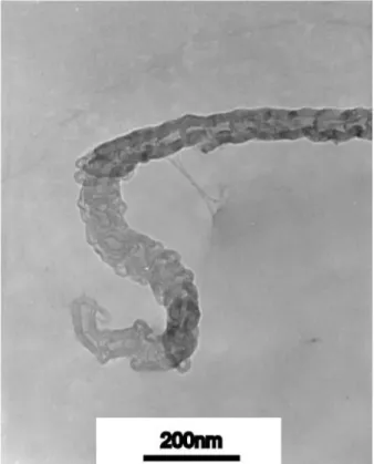
Fig. 3. TEM image of sample 5 carbon nanotubes with Co–Ni catalyst.
nm in diameter on average. Its SEM morphology is shown in Fig. 2a, where the right-bottom corner of the film was scratched. The figure indicates that the nano-tubes are almost perpendicular to the substrate surface, and only tube heads are visible from the top. In contrast, nested carbon nanotubes by applying Fe–Y catalysts have a diameters of ;30 nm and a length of a few micrometers, as shown in Fig. 2b. Compared to Fig. 2a, it indicates that introducing 10 vol.% elements Y into Fe catalysts increases both the longitudinal and trans-verse deposition rates, delaying the so-called ‘catalyst poisoning’ w14x. For the Co–Ni catalyst, Fig. 3 shows its TEM image of the tubes of ;40 nm in diameter and a few micrometers long in length. The alloy catalyst seems to yield a greater deposition rate than the pure element does, perhaps by lower activation energy for carbon atoms diffusing through the catalyst matrix. This suggestion is under investigation.
Interestingly, one nanotube can be divided into two parts, the smooth part and the worm-like part encapsu-lated with a catalyst particle, as shown in Fig. 3. The high degree of structure disorder or worm-like has been reported as being deposited at a relatively lower
tem-perature w15x, agreeing with results of our experimental setup, in which the temperature is initially low since the heating plasma source is far from the cooler substrate. Also, the change of nanotube from worm-like to straight shape is associated with a temperature rise of the catalyst particles, since they are pushed upward by growing nanotubes. Consequently, catalytic behaviors govern nanotubes growth in morphology, growth rates and structures.
3.3. Formation mechanism of the bamboo-like structure
According to chemical composition results, the sam-ples can be divided into group 1 (samples 1, 2 and 5)
and group 2(samples 3 and 4), where group 1 is carbon
nanotubes, and group 2 is Si–C–N nanotubes. Fig. 4 presents a typical TEM image of the bamboo structure of sample 3 from group 2. In the previous literatures, bamboo-like nanotubes using different catalysts, such as Fe, Ni, or Ni:Cu:Al alloy can be produced in many ways, including arc discharge w16x, microwave plasma CVD w17x and thermal pyrolysis methods w18x. There-fore, formation of bamboo-like structures seems to be independent of the deposition method and catalyst type. The proposed formation mechanisms of bamboo struc-tures, including open-ended growth w19x and stress-induced catalyst jumping w8x, seem unable to explain the results presented here. We propose that introducing
Fig. 4. TEM image of sample 3 Si–C–N nanotubes with Fe catalyst. Fig. 5. TEM image of sample 4 Si–C–N nanotubes with Fe catalyst.
Fig. 6. Raman spectra of samples 1 and 3.
N and Si atoms into the carbon nanotube structure may induce distortion; change the bonding in pentagonal, heptagonal or other crystal lattices, and promote bending stress. The stress may determine the compartment size of the bamboo structure that assertion is supported by the distorted bamboo-like structure shown in Fig. 5, in which more Si and N atoms are detected than nanotubes shown in Fig. 4. This stress-induced enhancement of deposition rate following such a high lattice distortion was demonstrated by a larger tube diameter (60–90
nm), as shown in Fig. 5. The arrows A and B in Fig. 4
correspond to the twisted nanotubes with catalyst and the defects of the tubes, respectively. The twist nanotube may also follow from the change in deposition directions due to lattice distortion caused by introducing Si and N atoms into the carbon nanotubes.
3.4. Effect of source gases on Raman spectra
Fig. 6 presents Raman spectra of the nanotubes using N gas2 (sample 3) to replace H gas (sample 1) as the2 source gases. Such spectra are multi-walled nanotubes and do not appear specific peaks of single-walled nan-otubes w20,21x. A much lower I yI ratioD G (s0.23) for sample 1 than for sample 3 (s0.78) reveals that more perfect nanotubes were formed using H gas. In addition,2 the higher I yI ratio and the slight up-shifts in peakD G positions for sample 3(Si–C–N nanotubes) agree with
the previous argument regarding lattice distortion of nanotubes, caused by introducing Si and N atoms to replace some C atoms.
3.5. CL properties
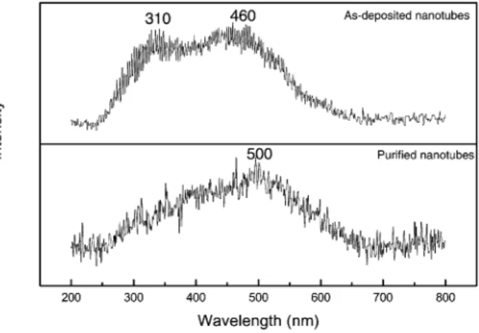
The as-grown nanotubes were annealed in an air furnace at 500 8C for 30 min to elucidate the CL emission of the purified Si–C–N nanotubes. Fig. 7 presents the CL spectra of the nanotubes before and after annealing. The figure shows an up-shift in peak
Fig. 7. CL spectra for as-deposited and purified Si–C–N nanotubes of sample 3.
Fig. 8.(a) J–E curves for samples 1–5, (b) current density vs. time
for carbon nanotubes of samples 1 and 2.
positions from 460 to 500 nm, and a decline in intensity of the 310 nm peak after annealing. This decrease implies that the emission at 310 nm can be partly removed by oxidation. The emission peak of 310 nm has been reported and may belong to amorphous, nan-oparticles or other defect bands w22x. In summary, purified nanotubes with 500 nm emission may have potential applications in blue light emission.
3.6. Field emission properties
Figure 8a depicts theJ–E curves for as-grown carbon
nanotubes and Si–C–N nanotubes. The emission current densities()10 mAyc m at 10 Vymm) of all nanotubes2 are much better than those of other field-emitting mate-rials. Carbon nanotubes(samples 1 and 2) exhibit better
emission properties superior to those of Si–C–N nano-tubes(samples 3 and 4), except sample 5. Low emission current of sample 5 could be related to worm-like part tube as previously mentioned, the reasons are not clear. Interestingly, the field emission properties of the nested carbon nanotubes (sample 2) are superior to well-aligned carbon nanotubes(sample 1).
According to the Fowler–Nordheim equation w23x, factors of work function (F), geometricenhancement
factor (GEF: b) and effective emission area (a) are
crucial for field emission property. Several other factors reported in Ref. w24x such as surface contamination, particles and protrusions and modification of materials after testing can drastically change field emission results. Also, the curvature of graphene sheets cause the decrease in energy barrier w22,25,26x. When the sheets bend, some sp hybridization of graphite may change to sp -2 3 like hybridization. This modification of atomic hybridi-zation is similar to negative electron affinity of diamond. A well-known result of NEA property on its surface is due to sp -hybridized carbons w22x. The nested nano-3 tubes belonging to highly bending structures can be
associated with more sp -hybridized bonding. Therefore,3 the nanotubes body themselves with NEA property contribute to field emission. We consider that both of larger emission area and more sp bonding for nested3 nanotubes are the reasons for higher emission current than well-aligned nanotubes. Otherwise, the screening effect due to neighboring nanotubes of well-aligned nanotubes with high density can lead to reduced GEF
w27x, this could be another reason for lower emission
current as compared to nested nanotubes.
However, the electron emission from well-aligned nanotubes is seemed to have a long lifetime. Fig. 8b compares the current density against time at constant electric field intensity (4 Vymm) for the well-aligned
carbon nanotube and the nested carbon nanotube, to determine the stability. The decay rate of the nested tubes is much steeper than that of the well-aligned tubes despite a greater current density at fist measurement. This result may follow from a weaker structure of nested tubes to stand in electric field. The collapse and damage of the tubes following SEM investigation support this suggestion.
4. Conclusions
Carbon and Si–C–N nanotubes were deposited suc-cessfully on Si wafers by MPCVD system. Using N to2 replace H2 for the source gases can form Si–C–N nanotubes rather than carbon nanotubes, and change the nanotube structures from a smooth wall to a bamboo-like structure. Nanotubes formed using additional Si sources exhibit(1) higher Si and N contents, (2) larger tubes and (3) more distorted bamboo-like structures. With respect to the formation mechanism of the bamboo-like structure of the Si–C–N nanotubes, introducing Si atoms into the carbon nanotube structure may change bonding and promote bending stress. This stress governs the compartment size of the bamboo-like structure. Field emission result also shows that higher current stability is achieved for well-aligned nanotubes than nested nanotubes.
The present conclusions indicate that a few materials can be introduced into nanotubes to change the proper-ties. The unique features of the nanotubes differing from the bulk properties have opened up many scientific and technological possibilities.
Acknowledgments
The authors would like to thank the National Science Council of Taiwan (contract no.:
NSC89-2216-E-009-020 and-019) and the Ministry of Education of Taiwan (contract no.: 89-E-FA06-1-4) for financially supporting
this research. References
w1x S. Iijima, Nature 354(1991) 56.
w2x P. Chen, X. Wu, J. Lin, K.L. Tan, Science 285(1999) 91. w3x C. Niu, E.K. Sichel, R. Hoch, D. Moy, H. Tennent, Appl. Phys.
Lett. 70(1997) 1480.
w4x G. Che, B.B. Lakshmi, E.R. Fisher, C.R. Martin, Nature 393 (1998) 346.
w5x S. Saito, Science 278(1997) 77.
w6x K.A. Dean, B.R. Chalamala, Appl. Phys. Lett. 75(1999) 3017. w7x W.B. Choi, D.S. Chung, J.H. Kang, H.Y. Kim, Y.W. Jin, I.T.
Han, Y.H. Lee, J.E. Jung, N.S. Lee, G.S. Park, J.M. Kim, Appl. Phys. Lett. 75(1999) 3129.
w8x M. Endo, S. Iijima, M.S. Dresselhaus(Eds.), Carbon
Nanotu-bes, BPC Press, UK, 1996, pp. 37, 159.
w9x H.L. Chang, C.T. Kuo, Diamond Relat. Mater. 10(2001) 1910. w10x A. Badzian, T. Badzian, W. Drawl, R. Roy, Diamond Relat.
Mater. 7(1998) 1519.
w11x L.C. Chen, C.T. Wu, J.J. Wu, K.H. Chen, Int. J. Mod. Phys.
B14(2000) 333.
w12x Z. Gong, E.G. Wang, G.C. Xu, Y. Chen, Thin Solid films 348 (1999) 114.
w13x J.Y. Wu, C.T. Kuo, T.L. Liu, Thin Solid films(2001) in press. w14x T.W. Ebbesen(Ed.), Carbon Nanotubes: Preparation and
Prop-erties, CRC Press, New York, 1997, p. 56.
w15x T. Baird, J.R. Fryer, B. Grant, Nature 233(1971) 233. w16x Y. Saito, T. Yoshikawa, J. Cryst. Growth 134(1993) 154. w17x H. Murakami, M. Hirakawa, C. Tanaka, H. Yamakawa, Appl.
Phys. Lett. 76(2000) 1776.
w18x D.C. Li, L. Dai, S. Huang, A.W.H. Mau, Z.L. Wang, Chem.
Phys. Lett. 316(2000) 349.
w19x D. Zhou, S. Seraphin, Chem. Phys. Lett. 238(1995) 286. w20x M.L. Terranova, S. Piccirillo, V. Sessa, P. Sbornicchia, M.
Rossi, S. Botti, D. Manno, Chem. Phys. Lett. 327(2000) 284. w21x Y. Ando, X. Zhao, K. Hirahara, K. Suenaga, S. Bandow, S.
Iijaima, Chem. Phys. Lett. 323(2000) 580.
w22x A.N. Obraztsov, A.P. Volkov, I. Pavlovsky, Diamond Relat.
Mater. 9(2000) 1190.
w23x C.A. Spomdt, I. Brodie, L. Humphrey, E.R. Westerberg, J.
Appl. Phys. 47(12) (1976) 5248.
w24x V.I. Merkulov, D.H. Lowndes, L.R. Baylor, S. Kang, Solid
State Electron. 45(2001) 949.
w25x H. Hiura, T.W. Ebessen, J. Fujita, K. Tanigaki, T. Takada,
Nature 367(1994) 148.
w26x J. Robertson, Diamond Relat. Mater. 5(1996) 797.
w27x V.I. Merkulov, D.H. Lowndes, L.R. Baylor, J. Appl. Phys. 89 (2001) 1933.