Influence of barrier growth temperature on the properties of
InGaN/GaN quantum wells
Tzu-Chi Wen**a, ShihChang Leea, Wei-I Leea,
aDepment of Electrophysics and Microelectronics and Information Systems Research
Center, National Chiao Tung University, HsinChu, Taiwan.
ABSTRACT
This study invests the effect of barrier growth temperature on the properties of InGaN/GaN MQW. Increase the growth temperature will reduce the well thickness and result in the blue shift of the PL peak. This blue
shift in PL peak wavelength may be resulted from the stain occure during varying barrier growth
temperature rather than only the reduce the well width. Moreover, we introduce a phase separation enhance layer into InGaN/GaN MQW. This layerjoin with the variation ofbarrier growth temperature will enhance the phase separation in InGaN/GaN MQW. There are two peaks clearly revealed in RT PL spectra. The higher energy peak might originate the InGaN quasi-wetting layer on the GaN barrier surface. The other one is interpreted of localize state at potential fluctuation owning to phase separation.
Keyword: InGaN/GaN multiple quantum well, barrier growth temperature, strain, phase separation, phase separation enhance layer, multi-peak.
1. INTRODUCTION
Group Ill-nitrides are highly promising for applications from green to ultraviolet light-emitting diodes (LED)11'21 and laser diodes (LDs)131, because of the wide bandgap varying from 1.9eV, of InN, to 6.3eV, of A1N. The InGaN and InGaN/GaN multiple quantum wells (MQW) have been used as the active layer for
these optoelectronic devices. Although the successful achievement in Nitride-based devices, the progress of blue and green laser diodes are often limited by the fundamental problems of InGaN. First of all, the low
miscibility of InN in GaN [41leadsa low growth temperature (below 1000°C) to obtain a higher indium mole fraction of InGaN films. However, this lower temperature usually accompanies with the poor crystalline quality of the epilayer. At this low temperature, the decomposition rate of ammonia (NH3) is so low that InGaN grown at this temperature tend to lack of nitrogen atoms. It is known that, the higher equilibrium vapor pressure of the nitrogen is required to prevent the dissociation of the In-N bond. Furthermore, the formation of indium droplet at temperature below 800°C become the other problem of growth InGaN [5]•
Kelleret al. have been reported that an extremely high V/Ill ratio is required to prevent the formation of
indium droplet [6]
Moreover,much interest has been focus on the InGaN/GaN MQW. Several groups have discussed the growth condition of the InGaN/GaN MQWs. Keller et al. reported the effect of the growth rate and barrier doping on the properties of InGaN/GaN [7]Uchidaet al. reported how the growth interruption affects the
crystalline quality of InGaN/GaN MQW [81• Harriset al. showd the different growth parameters, including the NH3 flow rate, hydrogen flow rate, total reactor flow rate and TMI flow rate, affect the
phtoluminescence properties of InGa1N/InGa1N MQW [9]However, there is no reported about the effect *
the barrier growth temperature on the properties of InGaN/GaN MQW.
The conventional method to growth the barrier layers and well layers of multiple quantum wells in ITT-V compound semiconductor is controlling the alkyl source flow into reactor or not. This is because the optimized growth conditions, including growth temperature, pressure and ambient, ofbarrier and well layers are very similar. However, the growth of multiple quantum wells in TIT-Nitrides is much more difficult. As mention above, owing to the low miscibility of InN in GaN, lower growth temperatures are required for the indium-contained nitrides. This lower temperature usually results in very poor crystalline quality. In addition, the growth temperature of GaN is required exceed 1000°C .Togrowth the GaN barrier in InGaN/GaN MQW at such low temperature will result in degradation of optical properties of MQW as well. Therefore, we try to increase barrier growth temperature and discuss how the growth temperature affects the optical properties of the InGaN/GaN MQW.
Furthermore, the emission mechanism of InGaN/GaN MQW is remaining unclear owning to the complex material physics. Such as the quantum confined Stark effect due to the piezoelectric field in strained wurtzite
InGaN/GaN MQW [10H141 phaseseparation results in a large fluctuation of indium in InGaN/GaN
MQW"5'20. Phase separation of InGaN/GaN is that local potential fluctuation due to a partial phase separation of InGaN in to GaN and InN [2h]•Severalgroups have been repoted the cross-section TEM
observations on the dot-like structure [19j•Theroom temperature (RT) photoluminescence (PL) of InGaN/GaN MQW and electroluminescence (EL) of MQW LEDs observed the multiple peak properties have been reported by Tran et al. 221Pozina et al. recently elucidated the origin of multiple peak PL [23]•They suggested the PL originated from (i) the MQW exciton recombination, (ii) the localized exciton in quasi-dot region owning to fluctuation of indium, and (iii) the surface defects induced zero-dimensional quantum islands. Although several reported concentrated on the phase separation in InGaN/GaN MQW, there are a few studies on the effect of QWs growth condition on phase separation.
This study invests the effect ofbarrier growth temperature on the properties of InGaN/GaN MQW. Increase the growth temperature will reduce the well thickness and result in the blue shift ofthe PL peak. Moreover, we introduce a phase separation enhance layer (PSEL) into InGaN/GaN MQW. This layer joined with the variation of barrier growth temperature will enhance the phase separation in InGaN/GaN MQW.
2. EXPERIMENT
InGaN/GaN MQW were grown on a sapphire (000 1) substrate by low pressure metalorganic chemical vapor deposition (MOCVD) in an EMCORE D180 system. The pressure ofgrowth was carried out at 100-300 ton. N2 and H2 was used as carrier gas. Trimethylgallium (TMGa), Trimethylindium (TMIn), ammonia (NH3) and silane (SiH4) were used as Ga, In, N, and Si sources, respectively. The substrate was initially heated to
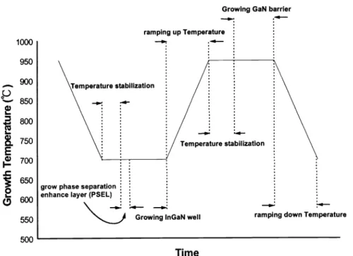
1080°C in the hydrogen ambient for 1 mm and then lowered to 51000 to grow the GaN nucleation layer. Next, the temperature was elevated to 1020°C in order to grow 2 pm unintentional doped buffer GaN. Finally, the temperature ramp down to the 700-900°C to grow InGaN/GaN MQW structures. To enhance the indium incorporation efficiency into InGaN well layers, the carrier gases were changed from H2 to N2. The growth temperature of InGaN well was 700°C ,andthe temperature of GaN barrier layer were ranged from 700°C to 950°C .TheMQW structure was terminated with an undoped GaN barrier layer. Linear ramp up or down the temperature was used in this study. Figure 1 displays the sequences of the temperature ramping process during growing InGaN/GaN MQW. The temperature stable time was necessary after ramping up or ramping down the temperature. The PID value of temperature controller was optimized for varying
temperature. The sources flow rate for each MQW samples are the same. The silane flow rate was controlled to achieve a doing concentration to 3x1017cm3 during GaN barrier growth.
Each sample was characterized by double-crystal x-ray diffractometer and room temperature (RT) photoluminescence (PL) measurement to determinate the crystalline quality and the In mole fraction in MQW structures. PL was measured at room temperature with a 325nm line of a He-Cd laser. The InGaN/GaN MQW for non-varied barrier growth temperature sample consist 10 periods of 3 nm thick InGaN well layers and 10 nm thick GaN barrier layers.
1000 950 900
0
'— 850800
.750
700
650
(p600
550 fv1Figure1 displays the sequences of the temperature ramping process during growing InGaN/GaN MQW.
Relative Diffraction Angle (arcsec)
Figure 2 illustrate (0002) reflection double-crystal X-ray diffraction of 10 period InGaN/GaN MQW structures with and without varying the barrier growth temperature.
Growing GaN barrier
ramping up Temperature
\emperature
stabilization
Temperature stabilization
_
-Growing inGaN well ramping down Temperature
Time GaN (0002) non-yarned barrier growth temperature -2
I
U) C U) C C >' >: -5000 -4000 -3000 -2000 -1000 0 1000 2000Figure 2 illustrate (0002) reflection double-crystal X-ray diffraction of 10 period InGaN/GaN MQW structures with and without varying the barrier growth temperature. The strongest peak is resulted from GaN buffer layer. Both samples reveal high-order satellite diffraction peaks. The satellite peaks arise from the periodicity of the quantum well superlattice. The quantum well superlattice period could be determined form the positions of these satellite peaks by Eq (1)
A
(2A6 . cos9B)
whereL is the summation of well and barrier thickness, X is x-ray wavelength, EO is the angle difference of two adjacent satellite peaks, and 0B is Bragg angles of (0002) GaN. Calculated the superlattice period of non-varied barrier growth temperature MQW samples and varied barrier growth temperature are 13.2 nm and 12. 8 nm, respectively. C, Cd) C a) C -J
0
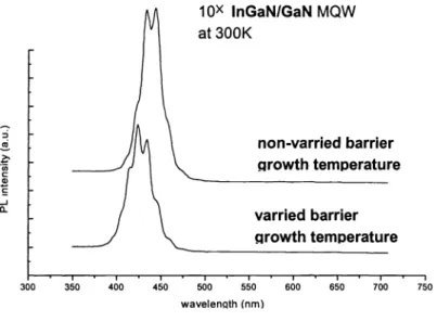
300Figure 3 is the RT PL spectra oflnGaN/GaN MQW with and without varying barrier growth temperature.
Figure 3 show the RT PL spectra of InGaN/GaN MQW with and without varying barrier growth temperature. The PL spectrum of the non-varied barrier growth temperature sample display a strong sharp peak at 443 nm with a FWHM of 27 nm. The indium mole fraction of InGaN well layer for this sample is 24% determined by PL measurement. However, the PL spectrum peak of varied barrier growth temperature one shift to 424 nm with a FWHM of 31 nm. The indium mole fraction of this one is only 19% by PL measurement.
lox InGaNIGaN MQW at 300K non-yarned barrier growth temperature 350 400 450 500 550 600 650 700 750 waveIenth (nm)
1000 950 900
0
850 800a
750E
700 550 500Figure4 displays the sequences of the temperature ramping process during growing InGaN/GaN MQW with phase separation enhance layer.
350 400 450 500
Wavelength (nm)
Figure 5illustratesthe RT PL spectra of InGaN/GaN MQW with PSEL. This layer was located between barrier and well
layers.
Growing GaN barrier
ramping up Temperature
—
Temperature stabilization
-Temperature stabilization
grow phase separation
enhance layer (PSEL)
-N..J Growing InGaN well ramping down Temperature
650 600
Time
B
A
lOx InGaN/GaN MQW with Phase Separation Enhance Layer (PSEL) at 300K
well grow 6 sec
CU > U, C C -J
0
300ellgro,1row18
sec 550 600 650 700 750Figure 4 displays the sequences ofthe temperature ramping process during growing InGaN/GaN MQW with phase
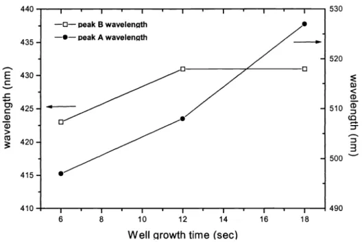
separation enhance layer (PSEL). This layer was located between barrier and well layers. Thus the total growth process was : (a). growing the PSEL; (b). growing the InGaN well layer; (c). ramp up the temperature; (d). growing the GaN barrier layer; (e). ramping down the temperature; (f). growing InGaN well layer. Figure 5 show the RT PL spectra of InGaN/GaN MQW with PSEL. Three different well growth time (well width) samples were invested in this study. The other growth condition including the well and barrier growth temperature, the temperature ramping rate, source flow rate, and period number were all the same. There are two peaks clearly revealed in this spectrum (denoted as peak A and Peak B). For the sample of well grow 18 sec, peak A located at 43 1 nm with higher PL intensity. This 43 1 nm peak corresponds to indium mole fraction of 21%. Moreover, peak B at 527 nm was much broad and lower PL intensity. This 527-nm peak
corresponds to In mole fraction of42%. Table 1 shows the all data ofthree samples. Figure 5 displays the
PL peak wavelength as a function of well growth time.
PeakA
Peak B Well growth time (sec)Peak
wavelength (nm) (eV)Corresponds
indium molefraction (%)
Relative peak intensityPeak
wavelength (nm) (eV)Corresponds
indium molefraction (%)
Relative peak
intensity
18 431 (2.88) 21 0.025 527(2.35) 42 0.021 12 431 (2.88) 21 0.03 508 (2.44) 39 0.021 6 423 (2.93) 19 0.08 497 (2.49) 37 0.191Table 1 shows the peak wavelength and relative peak intensity of samples with PSEL.
440 . . .
.
.
. . . .E430
-n t.J 0)) 425
510 0)(0
42O
435 530 520 —0— peak B wavelength —.— peak A wavelength:
415 500 490 I I 'I
• II --'
6 8 10 12 14 16 18Well cirowth time (sec)
(0002)
well qrow 6 sec U) C
-
wellqrowl2sec
U) C a) C>
)
well grow 18 sec-5000
'
-4cOO -3000 • -2000 • -1000 0 1000 2000 3000RelativeDiffraction Angle (arcsec)
Figure6 illustrate the (0002) reflection double-crystal X-ray diffraction of 10 period InGaN/GaN MQW structures with
PSEL.
Figure 6 illustrate the (0002) reflection double-crystal X-ray diffraction of 1 0 period InGaN/GaN MQW structures with PSEL. All these samples reveal high-order satellite diffraction peaks. The zero-order diffraction peak, of well grow 1 8 see, corresponds to an average indium mole fraction of 9%. This average indium composition also corresponds to 23% indium in the InGaN well layer.
3. RESULTS AND DISCUSSION
The MQW period is decreased while we increase the barrier growth temperature as illustrating in Fig. 2. However, the source flow rate and well and barrier growth times are all the same for both samples. Thus the
decrease indicates the well or barrier layer be etched as varying the growth temperature. We suggest the InGaN well layer might be etched more easily than GaN barrier layer. The growth temperature of InGaN well layer was 700°C, and the growth temperature of GaN barrier layer was up to 950°C. Supposing the annealing temperature higher than growth temperature, the semiconductor surface would slightly decomposition. On the contrary, the surface would not decomposition if the annealing temperature lower than growth temperature. Therefore, we interpret the InGaN well layer is etched during the temperature ramping up.
As to fig. 3, the PL peaks wavelength shift from 443 nm to 424 nm as increasing the barrier growth temperature. As mention above, the InGaN well layer might be etched as ramping the growth temperature.
Calculating the effective bandgap change as the well width reduce 0.4 nm by Eq. 2
E =
(ii2n2,r2)
(2
2m*L2
lox InGaN/GaN MQW with phase separation enhance layer 0
where i
isPlanck's constant, m* effective mass and L is quantum well width. It is only 0.95 meV inbandgap change as reducing the well width 0.4 nm. However the PL spectra display the peak wavelength shift 134 meV. Furthermore, suppose the purely well width reduces result in the PL peak wavelength shift, the FWHM should be decreased as reducing the well width as indicated from the previous report. On the contrary, the FWHM increase 4 nm in the varied barrier growth temperature sample. Unknown factors affect the optical properties of MQW as increasing the barrier growth temperature. It has been reported that the lattice mismatch and the difference in the thermal expansion coefficient between the InGaN and the GaN layer resulted in the stress in InGaN layer. Varying the barrier growth temperature during growing MQW might increase or decrease this strain. In addition, this strain will cause bandgap widening or narrowing in InGaN layer. Therefore, the blue shift in PL peak wavelength might be caused by the stain arise from varying barrier growth temperature rather than only the reduce the well width. The mechanism of this strain
is still unclear. Further study is required to completely understand the effect ofthis stain.
While epilayer growth on a substrate, it occurs in three distinct modes1241. Suppose the large strain energy between the substrate and the grown material, the Stranski-Krastanow (5K) growth mode will dominate. Foj
5K growth mode, a several-monolayer thin film, called a wetting layer, initially growth on the substrate surface. Then some cluster nucleation and form three-dimension island. In the InGaN/GaN MQW, large lattice constant difference produces strain energy between InN and GaN. Therefore, 5K growth mode is suggested to dominate in InGaN/GaN MQW. In Fig. 5, peak A does not markedly shift as the well growth time vary from 18 sec to 12 sec and slightly shift 7 nm as the well growth time reduce to 6 sec. This finding
implied that peak A is not sensitive to well width. Moreover, the peak wavelength ofpeak A is corresponds
to an indium composition of2l%, which is very close to the 23% determined form x-ray diffraction. Thus
peak A might originate the InGaN quasi- wetting layer on the GaN barrier surface.
Furthermore, peak B shift to low energy as increasing the well growth time implies that peak B is resulted from well-sensitive emission. As mention above, large lattice constant difference between InN and GaN will lead the indium segregation and phase separation. Increasing the well growth time will increase the InGaN cluster nucleation on the quasi-wetting layer surface. Therefore red shift in PL spectra is found as increasing
well growth time. The broaden ofpeak B in Fig. 5 indicates the distribution oflnGaN island is not uniform.
The origin of these two peaks is still unclear. Further and carefully study is required for understanding.
4. CONCLUSION
In summary, this study invests the effect of barrier growth temperature on the properties of InGaN/GaN MQW. Increase the barrier growth temperature will reduce the well thickness and result in the blue shift of the PL peak. This blue shift in PL peak wavelength might be owning to the in-plane tensile stain in varied barrier growth temperature rather than only the reduce the well width. Moreover, we introduce a phase
separation enhance layer (PSEL) into InGaN/GaN MQW. This layerjoined with the variation of barrier growth temperature will enhance the phase separation in InGaN/GaN MQW. There are two peaks clearly revealed in RT PL spectra. The higher energy peak might originate the InGaN quasi-wetting layer on the GaN barrier surface. The other one is interpreted of localize state at potential fluctuation owning to phase separation. However, the origin of these two peaks is still unclear. Further and carefully study is required for understanding.
ACKNOWLEDGMENTS
The authors would like to thank the National Science Council and of the Republic of China for financially supporting this research under Contract No. NSC 89-21 12-M-009-057.
REFERENCE
1. 5. Nakamura and G. Fasol, The Bule Laser Diode (Springer, Berlin, 1997).
2. 5. Nakamura, M. Senoh, N. Iwasa, and S. Nagahama, Jpn. J. Appl. Phys., Part2 34, L797 (1995).
(6661 SSOJd
ouopov)
so
wnutrnOsy,'syuj
pojqinossy-jpg
''ns
ninsij
j
LL9Z (000z) '(c) 88W1
jdd
j
'isjy
.j
pu
ouuy
H
'inii
i.
'JUJu!
put
'uiuiio
d
i
'u!zod
o
z
i
'uuoN
j
'uosn
a
'JS
Si(I3
'IjMOJ9 c61 L6E (8661)'uM0IH •D •JA •J 1TI
A
'10JA
A'iSU!SO
•V 'uI1LInqovi
•ir
)po1J)1
•d.I
UUj
•y
•j
6661 DEEdSM 'SJOOflpUOO!U1Sp1oi
pui
P!14!UUifl!j9
JO SUO!3ijddE pUEuissoooid
'SOflJOdOJd'I°°M
UtflS!1q3pu
'oumy
H
'PtSW
•I'!3S
(Xqoj)inus
'ip
H
SOIUf (L661) 9tEZ'IL
W1
Siq
iddy
'tJnwj
•s'pE
'nqiqoiqj
s
.oz (L661) 186 'OLW1
SX4djddy
'inmj
s
'!1d
s'oun
j,s'im
A
'tputu
A
61 (L661Y88Tt '69fl'1
SXq
jddy
'EJnw
•s
'EoSL
'tPV
L
'nq!q!q3
S
8I
(L661) 6801 'OLW1
Siq
1ddy'outuoj
j
pu
'spsnoj,
j
j
'ipndEjddo
J
'qui
j
LI (cL6T)zi
9j7 SAq jddyj
Apu
S'EJflWS
9J (9661)£L9i'c
SXq
jddy
ç
ud
'PbS
Ut
'rj
j
'iqstqjj
N
'nsDjno)
(6661)Lzo
ISi
S>J •puoo!Iuos °P!'UM •1OUJUI
SllA
'1flWIN
S'StUJ
d •S'PM
•)I':og
j
'nq!qo!q3 •dS
N
UUdS 'UUOOJA'Jnoqsug
'OOUJd (8661)86
°°S
SOJ