Influence of V/III Flow Ratio on Growth of InN on GaN by
PA-MOMBE
Wei-Chun Chen,aJr.-Sheng Tian,aYue-Han Wu,aWei-Lin Wang,aShou-Yi Kuo,bFang-I Lai,c and Li Changa,z
aDepartment of Materials Science and Engineering, National Chiao Tung University, Hsinchu, Taiwan bDepartment of Electronic Engineering, Chang Gung University, Kwei-Shan, Tao-Yuan, Taiwan cDepartment of Photonics Engineering, Yuan-Ze University, Taiwan, Chung-Li, Taiwan
InN epilayers were prepared on c-GaN/sapphire substrates by plasma-assisted metal-organic molecular beam epitaxy using N2
and trimethylindium precursor as the V/III sources. We studied the influence of the V/III flow ratio on the film structure, surface morphology, film compositions, and optical and electrical properties using scanning electron microscopy (SEM), atomic force microscopy (AFM), transmission electron microscopy (TEM), X-ray diffraction, X-ray photoelectron spectroscopy (XPS), secondary ion mass spectrometry (SIMS), photoluminescence (PL) measurement and Hall effect. The results show that epitaxial InN films can be obtained with the V/III ratio in the range between 1.81 and 4 at 500◦C. The InN growth rate decreases from 1.9 to 1.4μm/h when the ratio increases from 1.81 to 4. The surfaces of the InN films are not smooth in the V/III range used. Cross-sectional TEM revealed that the planar defect density in InN is as high as∼ 1.5 × 106cm−1at a V/III ratio of∼1.81. XPS and SIMS results show
that the film surface contains oxygen, which is found to affect the measured carrier mobility and concentration. © 2013 The Electrochemical Society. [DOI:10.1149/2.011307jss] All rights reserved.
Manuscript submitted January 30, 2013; revised manuscript received April 11, 2013. Published May 17, 2013.
Indium nitride (InN) is an attractive material for electronic and op-toelectronic applications because it has many outstanding properties,1
such as a small effective mass2 and the recently discovered small
bandgap of approximately 0.7 eV.3 InN has attracted intensive
re-search interest mainly because of its possible applications in high-speed/high-frequency electronics1and terahertz emission.4Above all,
the narrow bandgap of InN allows III-nitride ternary alloy systems to extend their spectral range from infrared to deep ultraviolet, which is advantageous, e.g., for multi-junction solar cell devices.5Further, the
electron mobility at room temperature can be more than 2100 cm2/V
s with a residual carrier concentration of close to 8× 10¹⁷/cm3.6The
previously measured energy gap values of the InN were in the range of approximately 1.8–2.1 eV. This could be attributed to the presence of In2O3 (Eg = 3.75 eV)7 inclusions and perhaps to a blue-shift of
the absorption-edge quantum-size effects caused by the needle-like crystallite structure.3
Most of InN samples available today have been grown using metal-organic chemical vapor deposition (MOCVD),8molecular beam
epi-taxy (MBE),9and pulse laser deposition (PLD).10However, the growth
of a high-quality InN film remains a challenge because InN has a low dissociation temperature of about 600◦C.11The growth temperature
is thus limited by the desorption of nitrogen and the thermal decom-position of the films.12
Sapphire has been widely used for the heteroepitaxial growth of InN, even though it is an insulator and has a large lattice mismatch with InN (∼25%). However, various types of buffer layers, such as InN,13AlN,14and GaN,15have been found to be critical for the growth
of high-quality InN films. InN has been grown on an AlN buffer layer grown on a (0001) sapphire substrate.16For the growth of high-quality
InN, GaN has been used as the buffer layer17primarily because the
lattice mismatch is small (∼9%) in this case.
Previous studies of InN deposition on GaN have shown that InN has good crystallinity. Wang et al. reported18the effect of flow ratios
on the morphology of InN grown by radio-frequency (RF) plasma source molecular beam epitaxy (RF-MBE). Moreover, earlier litera-ture suggests that a precise control of the In/N fluxes can facilitate the growth of high-quality InN.19It has also been indicated that the
growth of InN by MBE is very sensitive to the V/III ratio.20 The
V/III ratio may also impact the incorporation of other unintentional impurities such as hydrogen and oxygen.21In addition, Laboutin et al.
indicated that the density and size of InN islands along with their struc-tural and optical properties are strongly influenced by the properties of the underlying GaN buffer layer.22Plasma-assisted metal-organic
zE-mail:[email protected]
molecule beam epitaxy (PA-MOMBE) is a relatively newly developed growth method which combines characteristics of both RF-MBE and MOCVD techniques. Due to the limitation of low-dissociation tem-perature and high N2equilibrium pressure over InN, plasma-assisted
MBE has been thought to be suitable for the InN growth.23,24Previous
studies of MOMBE growth GaN materials have shown the growth rate below 0.3μm/h.25However, the growth rate of InN grown by
conventional MBE is close to 1μm/h, whereas PA-MOMBE may al-low the deposition of InN at high growth rate of more than 1μm/hr.26
In the past, only few studies have reported the InN growth using PA-MOMBE technique.27However, control of PA-MOMBE deposition
conditions is still required for obtaining better crystal quality. In this paper, we report the effect of varied V/III flow ratios on properties of InN films grown on GaN template by PA-MOMBE. Structural characterization of the grown films shows that the crys-tallinity of InN depends significantly on the V/III ratio.
Experimental
InN films were grown on GaN/Al2O3 substrates using
PA-MOMBE with the background pressure of 1.33 × 10⁻⁷ Pa.
Trimethylindium (TMIn) without any carrier gas was used for group-III precursor. For the group-V source, N2gas (99.9999%) before
flow-ing into the chamber was decomposed to atomic nitrogen by applyflow-ing a RF plasma. Commercially available substrates used in this study consisted of 4μm thick c-plane GaN buffer layer grown on c-plane sapphire by MOCVD. Before the growth of InN, the substrate was thermally treated at 550◦C for 20 min in vacuum, followed by nitrida-tion at 550◦C for 10 min with RF plasma of N2gas at 1 sccm. During
the InN growth, the gas flow and the reactor pressure were maintained constant. The RF power was maintained at 350 W with a N2gas flow
rate of 1 sccm (corresponding to 1.33 × 10⁻³ Pa). The InN films were grown at various TMIn flow rates for 30 min. In our previous study of PA-MOMBE growth of InN epilayer on GaN buffer layer,28
we found that the optimum temperature for the growth of high-quality InN films was 500◦C. Therefore, the nominal growth temperature (TG) at 500◦C was used in the present study for the epitaxial growth of InN films on the GaN template for all the grown films. Structural prop-erties of the InN epilayers were characterized with X-ray diffraction (XRD) using a Cu Kα X-ray line (XRD, Siemens D5000). The full widths at half maximum (FWHMs) of theω-scan rocking curves of the InN films measured with high-resolution XRD (Bede D1) were used for evaluating the crystallinity. 2θ scan from 23◦to 40◦with step size of 0.005◦in XRD was performed for determining the lattice pa-rameters. Observations of surface morphologies and microstructures
P306 ECS Journal of Solid State Science and Technology, 2 (7) P305-P310 (2013)
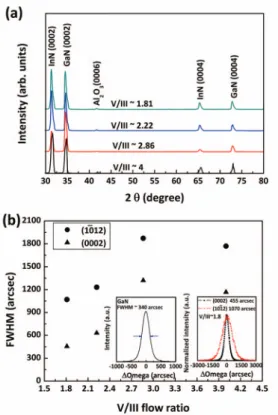
Figure 1. (a)θ-2θ XRD patterns of InN films deposited on GaN with various V/III ratios. (b) FWHMs of (0002) and (1012)ω-scan XRCs of InN samples grown with various V/III ratios. Inset figures showing the XRC of GaN buffer layer and InN film growth on GaN with V/III∼ 1.81.
of the films were performed in a field-emission scanning electron microscope (SEM, Hitachi S-4300) and a transmission electron mi-croscope (TEM, Philips Tecnai 20). Cross-sectional TEM specimens were prepared by using the focused ion beam technique. The surface morphologies of the layers were also analyzed with atomic force mi-croscopy (AFM) using a Vecco di-D3100 system in tapping mode. The photoluminescence measurements were obtained at 10 K using a diode-pumped solid-state laser of 532 nm wavelength as the excita-tion source. In order to obtain the distribuexcita-tion of chemical elements in the InN films, the depth profiles were acquired from a secondary ion mass spectrometer (SIMS, CAMECA IMS-6f) with a Cs+ion beam for negative ions and an O2+ion beam for positive ions. The X-ray
photoelectron spectroscopy (XPS) experiments were performed in a VG ESCA Scientific Theta Probe using Al Kα (hν = 1486.6 eV) ra-diation to characterize the bonding characteristics of elements in the films. The electrical properties were assessed on the basis of the Hall effect measurements using the van der Pauw configuration at room temperature.
Results and Discussion
Figure1ashows the XRDθ-2θ scans for the samples grown at the V/III flow ratio of 4, 2.86, 2.22, and 1.81. The XRD patterns of all the deposited InN films with different V/III ratio show that the prominent peaks of InN film, GaN buffer, and sapphire substrate are clearly resolved. All the InN films are preferentially oriented in the c-axis direction. In addition, no metallic In peaks are observed in the patterns, implying that the V/III ratios used for the deposition are appropriate for the TMIn precursor to completely react with nitrogen. The measured rocking curve patterns of the InN (0002) from the samples showed in Fig.1bexhibit the FWHMs in the range of 455–1167 arcsec among which the sample grown with the V/III ratio of∼1.81 has the smallest value of 455 arcsec, suggesting that the film quality is reasonably good. The (0002) full-width half maximum (FWHMs) values of all
the InN films are higher than that of the GaN layer (∼340 arcsec), probably caused by a relatively large number of defects in InN. In addition, the results indicate that the FWHMs values in the (1012) direction increases from 1070 to 1170 arcsec when the V/III flow ratio increases from 1.81 to 4. However, it is known that the FWHMs of both the symmetric (0002) and the asymmetric (1012) X-ray rocking curves increase with an increase in the threading dislocation (TD) density for screw and edge dislocations, respectively.29 Also, XRD
can be used to quantify the TD density. The dislocation density can be evaluated using the formula:30
N= α
2
4.35b2 [1]
whereα is the tilt or the twist angle were determined by the FWHM of symmetric and asymmetric rocking curves, and b is the magnitude of the Burgers vector. The determination of the tilt and twist angles is therefore essential to quantify the TD density in the sample. At the FWHM of theϕ rocking curve can be used as α indicator of the twist angle.31Thus, the FWHM of InN (1012)ϕ scans was used for
measurement the twist angle.
From the XRD rocking curves, the screw type dislocation densities for V/III∼1.81 to 4 can be estimated to be in the range of 3.8 × 10⁸
to 2.1× 109cm−2, and the edge one in 4.2–5.1× 1010cm−2. Also,
the smaller FWHMs of the InN (10 1 2) rocking curves are obtained with lower V/III ratios. This may imply that the dislocation density in the InN films can be reduced for growth with a low V/III ratio.
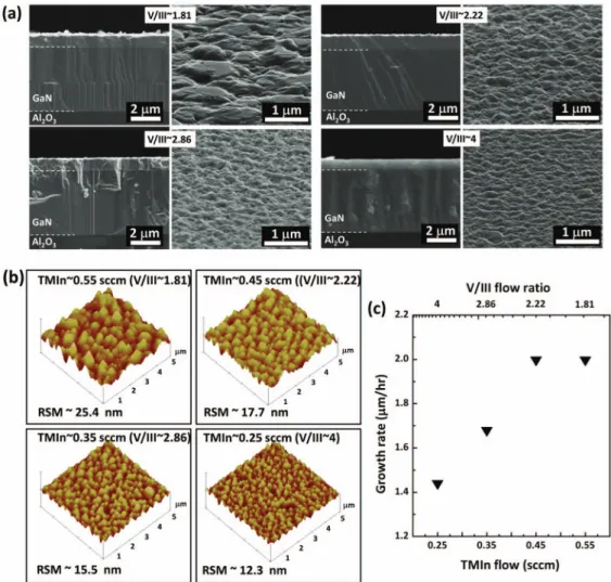
Figure2ashows cross-sectional and top-view SEM micrographs of the InN films grown with different V/III ratios. Also, AFM images included in Fig.2bto shows the surface morphology of the samples. It is clear that the film thickness of InN decreases from 1000 nm to 730 nm with increasing the V/III ratio from 1.81 to 4. Also, the root-mean-square (RMS) surface roughness values were measured from 5× 5 μm2AFM scans. The RMS surface roughness increases
mono-tonically from 12 nm for the V/III∼4 to 25 nm for the V/III∼1.81. The variation of the growth rate with the TMIn flow rate is plotted in Fig.2c. It is clearly seen that the growth rate increases from 1.4 to 2.0μm/h when the TMIn flow rate increases from 0.25 to 0.55 sccm corresponding the V/III ratio from 4 to 1.81. However, further increase of the TMI mass flow (V/III< 2.22) does not increase the growth rate, as the excess of In may not form InN bonds as a result of the deficiency of active nitrogen. However, in the V/III range used in the present study, all the film surfaces exhibit rough morphology probably due to the three-dimensional island growth mode.
As the InN film grown with 1.81 V/III ratio has the best crys-tallinity, the detailed characterization of this film by TEM, SIMS, XPS, PL, and Hall measurement will be presented in the following. Figure 3ashows a typical cross-sectional bright-field TEM image (near two-beam condition with g= 1120 of InN) for the InN/GaN structure deposited with V/III ratio of∼1.81. The InN film thickness is around 1000 nm. The surface profile of InN is rather rough similar to the SEM observation. In the InN film, no evidence for the existence of metallic-In inclusions can be found in consistence with the XRD result. Interestingly, it is observed that most of the TDs in the GaN do not cross the interface into the InN film. Therefore, most of the defects in InN are likely to form during film deposition or after 3D island coalescence. Figure3bshows a selected-area electron diffrac-tion (SAED) pattern from the InN film and GaN along the<1120> zone axis. It is clearly observed that the diffraction spots of InN and GaN are well aligned with each other, showing that InN is epitaxial with GaN. Furthermore, no extra diffraction spots can be observed in the pattern, suggesting that no interlayer reaction occurs between InN and GaN and no metallic In phase exists in InN in the nanometer scale. Moreover, it can be clearly observed that the InN spots in the SAED pattern exhibit sharp streaks along the direction of the c-axis, suggesting that there exist a high density of planar defects in the InN film.
Figure4shows TEM images at high magnification in the two-beam conditions with g= 0002 and g = 1100. In Figs.4athe TDs are
Figure 2. (a) SEM micrographs in cross-sectional view (left column) and top view (right column) of InN films grown with different V/III flow ratios. Fig. 2(b) shows the AFM images with various V/III ratios. (c) Plot of growth rate versus V/III flow ratio for InN films.
observed in the images with g= 0002. The planar defects are seen in Figs.4bas basal stacking faults (BSFs) and/or dislocation loops with an estimated density of approximately 1.5× 106 cm−1 for the
V/III ratio of∼1.81. Compared with the planar defect density often
Figure 3. (a) Cross-sectional TEM image and (b) the corresponding SAD pattern of InN/GaN interface deposited with V/III ratio of∼1.81.
observed in MBE-deposited GaN, which is in the order of 105cm−1,
the BSF density in the InN film is approximately one order of magni-tude higher. The speculated reasons for such a high density of BSFs might be caused by the clustering of vacancies and high impurity concentrations as shown later from the SIMS result.
An HRTEM image of the interfacial region between InN and GaN in [1120] with the corresponding fast-Fourier-transform pattern is shown in Fig.5. The (0002)InNlattice fringes are clearly observed with
the . . . ABABAB. . . stacking sequence, which confirms the wurtzite
Figure 4. Cross-sectional bright field TEM images of InN films grown with V/III ratio of ∼1.81 under two-beam conditions: (a) g = 0002 and (b) g= 1 100.
P308 ECS Journal of Solid State Science and Technology, 2 (7) P305-P310 (2013)
Figure 5. High-resolution TEM micrograph of InN/GaN interface. Fourier filtered lattice image showing misfit dislocations at∼2.76 nm spacing.
structure with the c lattice parameter of approximately 0.57 nm close to the value for the InN bulk crystal.32Moreover, an analysis of the
images indicates that BSFs change the perfect . . . ABABABAB. . . stacking sequence into the . . . ABABCBCB. . . sequence correspond-ing to the I1type of BSFs. The Fourier filtered image reveals the misfit
dislocations (MDs) at the InN/GaN interface; the shortest averaged distance between these dislocations is approximately 2.76 nm as a result of the lattice misfit (∼9%), in agreement with the theoretically calculated value. This result indicates that the MDs effectively accom-modate most of the misfit strain induced by the lattice mismatch.
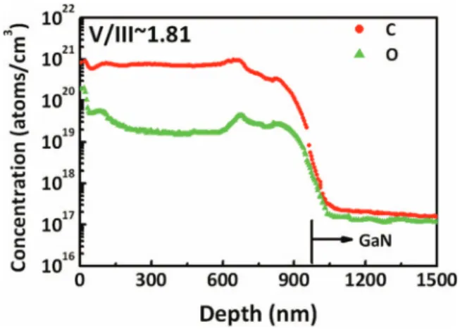
Figure6shows the SIMS depth profiles of the grown InN films for O and C distributions. To remove the effect of background pressure in the SIMS vacuum chamber on the measurement of these light element concentrations, a high-quality thick GaN sample was used for standard reference. The ion yield obtained from the standard sample was used to calibrate the O and C concentrations in the InN samples. The C impurities in the SIMS profile may be originated from the TMIn precursor. The carbon concentration in the grown film is in the order of 1021cm−3, which is the dominant source of unintentional donors
for the InN films. Iwao et al.33indicated that carbon is incorporated
as a background during PA-MOMBE growth, although the electrical properties were improved due to they prefer to form the CO and/or CO2 with oxygen atoms that have rather high vapor pressures. The
oxygen concentration in the InN film is about 2× 1019cm−3. It is also
Figure 6. SIMS depth profiles of InN films grown with V/III ratios∼1.81.
noticed from the SIMS profile that a relatively high O concentration exists near the surface of the InN film. This may be due to the H2O
absorption on the InN surface. Specht et al.34reported similar result for
impurity concentration in MBE-grown InN. As no diffraction spots from crystalline indium oxides can be found in the SAD patterns, the oxygen might exist as impurities or point defects in the film. Alternatively, they might cluster to form stacking faults. Carbon might behave similarly in the film.
Figure7ashows the In3d XPS spectra of the InN films obtained at various depths with V/III flow ratio∼1.81. As one can see in the spectra, the binding energies (BE) of In3d3/2and In3d5/2are 451.45
and 443.85 eV, respectively. The result shows that the difference in the BE of In3d3/2and In3d5/2is almost constant and equal to 7.6 eV
in agreement with the value in literature.35 Figure7bshows a
sur-face spectrum in which the In3d5/2peak can be deconvoluted to two
components with a BE difference of 1 eV after curve fitting. The first component has a BE of 444.2 eV, whereas the second component has 445.2 eV. The main peak observed at 444.2 eV can be interpreted to be an In–N bond. The shoulder peak at 445.2 eV can be attributed to the indium bound with oxygen which can be In2O3(BE≈ 444.6–
444.9 eV),36In–O–H (BE≈ 445 eV), and InO
x(BE≈ 445.1 eV).37
Oxygen 1s BE spectrum shows in the inset of Fig.7b. The strongly peak observed at 531.7 eV can be interpreted to be an OH bond38
from the InN surface. Therefore, the InN film has a high oxygen con-centration (1021cm−3) near the surface in agreement with the SIMS
results.
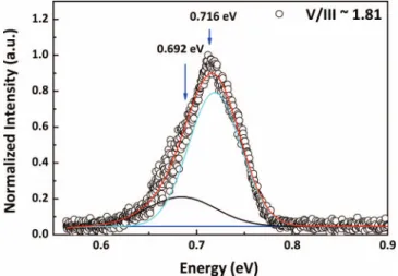
The PL spectrum in Fig.8shows an emission peak at 0.716 eV. The infrared peak is a typical characteristic for the high quality InN. However, the PL emission line shape of InN can be characterized as free-to-bound recombination between the degenerate electrons in the conduction-band and the photo-generated holes at the valence-band edge. The shape of the PL band can be analyzed according to the following expression19
I (¯hω) ∼ [¯hω − EG(n)]γ/2f (¯hω − EG(n)− EF) [2] where f is the Fermi–Dirac function, EG(n) is a carrier
concentration-dependent bandgap which approaches the bandgap EG(n)→EG(n) at
vanishing the electron carrier concentration n→0, γ is a parameter which increases from 2 to 4 with increasing concentration of free carriers in InN, and EFis the Fermi energy of the degenerate electrons.
The solid lines in Fig.8show the fitted PL spectrum of InN, revealing a good agreement between the fitting curves and the experimental data. The band-gap is estimated to be 0.692 eV and the Fermi level is 23.9 meV below the conduction band minimum. The band-gap value is close to the 0.67 eV for the high quality single crystalline InN materials.39
According to the SIMS result, the surfaces of the InN films have high C and O concentrations in the depth range of approximately 10 nm, which may influence the measurements of electrical proper-ties. In order to evaluate the effect of the C and O elements in the InN
Figure 7. XPS spectra of (a) In 3d and (b) In 3d5/2with depth peaks for the
InN film grown with a V/III flow ratio of∼1.81.
surface region on the electrical properties, the film surface was etched with 37% HCl for 80 s to remove the surface layer about 10–20 nm. Before etching, the film exhibits the high carrier concentration of 5.57 × 1019 cm−3, low mobility of 192 cm2/V-s and resistivity of 4.82
× 10−4 ohm-cm. After etching, the etched InN film exhibited a
de-creased carrier concentration of 3.31× 1019cm−3, increased electron
mobility of 335 cm2/V-s and resistivity of 5.50× 10⁻⁴ohm-cm.
Af-ter etching, the InN film grown with 1.81 ratio exhibits the highest Hall mobility and lower carrier concentration among all the grown InN samples. Therefore, the surface conditions with high oxygen and carbon concentrations may significantly affect the electrical proper-ties of the InN film. Similar results have also been shown by Gwo et al. for electrical properties of etched InN40,41and Soh et al. for Hall
measurement of Si-doped GaN.42
From the above results, it is shown that the V/III ratio for the growth of InN on GaN by PA-MOMBE has a significant effect on the film crystallinities, surface morphologies, and growth rate. A low V/III ratio may favor the InN growth of better quality. Furthermore, the InN films grown by PA-MOMBE may have a relatively higher density of BSFs and contain high impurity concentrations of C and O elements, compared with those grown by conventional MBE. Fur-thermore, the electrical properties are closely related with structural properties and film impurities. As a result, for high-quality InN grown by PA-MOMBE, further investigations still need to be done such as using other In-precursor, varying flow for enhanced interaction of In with N, and 2D growth, etc.
Figure 8. Measured (circles) and fitted (solid lines) PL of InN/GaN/sapphire measured at 10 K.
Conclusions
In summary, we have investigated the effect of the V/III ratio on surface, structural, optical, and electrical properties of InN epitaxially grown on GaN/sapphire by PA-MOMBE. Structural characterization by XRD and TEM shows that all the InN films grown with the V/III ratio in the range of 1.81–4.0 had good crystallinity without any metallic In phase. The InN film grown with V/III ratio of 1.81 has better crystallinity, higher mobility of 335 cm2/V-s, and a near-infrared
emission PL peak at 0.716 eV. Also, SIMS and XPS results show that C and O concentrations in the InN film and on the film surface play significant roles on electrical properties.
Acknowledgments
The authors would like to gratefully acknowledge partial financial support from the Ministry of Economic Affairs under Contract No. 99-EC-17-A-05-S1-154 and National Chiao Tung University (100W978, 101W978).
References
1. A. G. Bhuiyan, A. Hashimoto, and A. Yamamoto,J. Appl. Phys., 94, 2779 (2003). 2. S. N. Mohammad and H. Morkoc,Prog. Quantum Electron., 20, 361 (1996). 3. V. Yu. Davydov, A. A. Klochikhin, R. P. Seisyan, V. V. Emtsev, S. V. Ivanov,
F. Bechstedt, J. Furthm¨uller, H. Harima, A. V. Mudryi, J. Aderhold, O. Semchinova, and J. Graul,Phys. Stat. Sol.(b), 229, R1 (2002).
4. R. Ascazubi, I. Wilke, K. Denniston, H. Lu, and W. Schaff,Appl. Phys. Lett., 84, 4810 (2004).
5. J. Wu, W. Walukiewica, K. M. Yu, J. W. Ager III, E. E. Haller, H. Lu, W. J. Schaff, Y. Saito, and Y. Nanishi,Appl. Phys. Lett., 80, 3967 (2002).
6. M. Feneberg, J. Daubler, K. Thonke, and R. Sauer,Phys. Rev. B, 77, 245207 (2008). 7. R. L. Weiher and R. P. Ley,J. Appl. Phys., 37(1), 299 (1966).
8. C. Yang, X. Wang, H. Xiao, X. Zhang, G. Hu, J. Ran, C. Wang, J. Li, J. Li, and Z. Wang,Appl. Surf. Sci., 255, 3149 (2008).
9. J. Grandal, M. A. Sanchez-Garcia, E. Calleja, E. Gallardo, J. M. Calleja, E. Luna, A. Trampert, and A. Jahn,Appl. Phys. Lett., 94, 221908 (2006).
10. K. Fujiwara, A. Ishii, J. Ohta, H. Fujioka, and M. Oshima,Thin Solid Films, 464–465, 112 (2004).
11. M. Higashiwaki and T. Matsui,J. Cryst. Growth, 252, 128 (2003). 12. Q. Guo, O. Kato, and A. Yoshida,J. Appl. Phys., 73, 7969 (1993).
13. A. Amamoto, Y. Yamauchi, M. Ohkubo, A. Hashimoto, and T. Saitoh,Solid-State Electron., 41, 149 (1997).
14. H. Lu, W. J. Schaff, J. Hwang, H. Wu, G. Koley, and L. F. Eastman,Appl. Phys. Lett., 79, 1489 (2001).
15. F.-I. Lai, S. Y. Kuo, W. C. Chen, W. T. Lin, W. L. Wang, L. Chang, C. N. Hsiao, and C. H. Chiang,J. Cryst. Growth, 326, 37 (2011).
16. Y. S. Lin, S. H. Koa, C. Y. Chan, S. S. H. Hsu, H. M. Lee, and S. G. Gwo,Appl. Phys. Lett., 90, 142111 (2007).
17. C. J. Lu, L. A. Bendersky, H. Lu, and W. J. Schaff,Appl. Phys. Lett., 83, 2817 (2003). 18. H. Wang, D. S. Jiang, J. J. Zhu, D. G. Zhao, Z. S. Liu, Y. T. Wang, S. M. Zhang, and
H. Yang,Semicond. Sci. Technol., 24, 055001 (2009).
19. V. Y. Davydov, A. A. Klochikhin, V. V. Emtsev, D. A. Kurdyukov, S. V. Ivanov, V. A. Vekshin, F. Bechstedt, J. Furthmuller, F. Aderhold, J. Graul, A. V. Mudryi,
P310 ECS Journal of Solid State Science and Technology, 2 (7) P305-P310 (2013)
H. Harima, A. Hashimoto, A. Yamamoto, and E. E. Haller,Phys. Stat. Sol.(b), 234, 787 (2002).
20. Y. Nanishi, Y. Saito, and T. Yamaguchi,Jpn. J. Appl. Phys., 42, 2549 (2003). 21. N. Khan, A. Sedhain, J. Li, J.Y. Lin, and H. X. Jiang,Appl. Phys. Lett., 92, 172101
(2008).
22. O. A. Laboutin and R. E. Welser,Appl. Phys. Lett., 92, 223103 (2008).
23. S. J. Pearton, GaN and Related Materials, p. 433, Gordon and Breach, New York, (1997).
24. C. R. Abernathy, J. D. MacKenzie, and S. M. Donovan,J. Cryst. Growth, 178, 74 (1997).
25. T. Yaguchi, S. Yonemura, H. Tsuchiya, N. Shimoyama, T. Suemasu, and F. Hasegawa, J. Cryst. Growth, 189–190, 380 (1998).
26. W. C. Chen, S. Y. Kuo, F.-I. Lai, W. T. Lin, and C. N. Hsiao,Thin Solid Films, 529, 169 (2013).
27. J. Aderhold, V. Yu. Davydov, F. Fedler, H. Klausing, D. Mistele, T. Rotter, O. Semchinova, J. Stemmer, and J. Graul,J. Cryst. Growth, 222, 701 (2001). 28. W. C. Chen, S. Y. Kuo, F.-I. Lai, W. T. Lin, C. N. Hsiao, and D. P. Tsai,J. Vac. Sci.
Technol. B, 29, 051204 (2011).
29. B. Heying, X. H. Wu, S. Keller, Y. Li, D. Kapolnek, B. P. Keller, S. P. DenBaars, and J. S. Speck,Appl. Phys. Lett., 68, 643 (1996).
30. T. Metzger, R. H¨opler, E. Born, O. Ambacher, M. Stutzmann, R. St¨ommer, M. Schuster, H. G¨obel, S. Christiansen, M. Albrecht, and H. P. Strunk,Philo. Mag. A, 77, 1013 (1998).
31. H. Heinke, V. Kirchner, S. Einfeldt, and D. Hommel,Phys. Stat. Sol.(a), 176, 391 (1999).
32. T. L. Tansley and C. P. Foley,J. Appl. Phys., 59, 3241 (1986).
33. K. Iwao, A. Yamamoto, and A. Hashimoto,Phys. Stat. Sol.(c), 4, 2453 (2007). 34. P. Specht, R. Armitage, J. Ho, E. Gunawan, Q. Yang, X. Xu, C. Kisielowski, and
E. R. Weber,J. Cryst. Growth, 269, 111 (2004).
35. J. F. Moulder, W. F. Stickle, P. E. Sobol, and K. D. Bomben, in Handbook of X-ray
Photoelectron Spectroscopy: A Reference Book of Standard Spectra for Identification and Interpretation of XPS Data, edited by J. Chastain (Perkin-Elmer Corporation,
Physical Electronics Division, Eden Prairie, MN, 1992).
36. Y. Masuda, M. Kondo, and K. Koumoto,Crystal Growth & Design, 9, 555 (2009). 37. C. Schmide, T. Sowade, E. Loffler, A. Birkner, and W. Griinert,J. Phys. Chem. B,
106, 4085 (2003).
38. A. S. Lim and A. Atrens,Appl. Phys. A, 51, 411 (1990).
39. A. A. Klochikhin, V. Yu. Davydov, V. V. Emtsev, A. V. Sakharov, V. A. Kapitonov, B. A. Andreev, H. Lu, and W. J. Schaff,Phys. Rev. B, 71, 195207 (2005). 40. C. T. Kuo, S. C. Lin, K. K. Chang, H. W. Shiu, L. Y. Chang, C. H. Chen, S. J. Tang,
and S. Gwo,Appl. Phys. Lett., 98, 052101 (2011).
41. C. L. Wu, C. H. Shen, H. Y. Chen, S. J. Tsai, H. W. Lin, H. M. Lee, S. Gwo, T. F. Chuang, H. S. Chang, and T. M. Hsu, J. Cryst. Growth, 288, 247 (2006).
42. C. B. Soh, S. J. Chua, H. F. Lim, D. Z. Chi, S. Tripathy, and W. Liu,J. Appl. Phys., 96, 1341 (2004).