variable threshold function in order to eliminate the deadband. The others are used for attenuation using the weighted sum opera- tion of the FG-MOSFETs. When w, = wj,> = wi, from cqn. 2, V, of FMn
(5,J
and FhfP(V,)
are given byvfn = Kn(DOl01
+
011112 f D Z W 3 )+
W 4 % n (4)V f p = KrL(DoW1
+
DIWZ+
D ~ W Q )+
W 4 v B y ( 5 ) where Do.D 1
andD2
are the digitdl signals and are equal to I or 0. If V,,, 2 VT,,/w4 and1 VBpl
2I VTpl/w4
are satisfied: the polarities of V;,, and V & are changed, and so both FM, and FM, operate as depletion-mode MOSFETs. Consequently, the current operates as a Class AB circuit so that each conducts a small quiescent cur- rent for V , = 0. Therefore, the deadband can be e h n a t e d per- fectly. When we design V V ~ : W ~ : W ~ = 2":2l:2', from cqns. 4 and 5: the ideal V,,,, can be given by0.3 C . >- $0.2
P
0.1where IRI." is IxL at
V,,
= 0. From eqn. 6, the circuit operates as a digitally programmable Class AB attenuator.0.4 I I I I I I I 0 .
.
..
R
0 0 0 0 0 0 0 0 0 0-
000 001 010 011 100 101 110 111 (DZ, D1, Do)1501131
Fig. 3 Gain against ( D z , D,, Do)
0 without RL 0 RL = lOkQ I . o 2.0
E
/
1.01
0.5 0.5 1 .o 1.5 2.0 2.5 3.0 "in, "p-p1501141
Fig. 4 THD against input signal level -0- ( 0 2 , D,, Do) = (0. 0, I ) -A- (D2, DI, Do) = (1, 0, 0) -0- ( 0 2 ,
4,
D,) = (1, 1, 1)Simulation and experinzcxtul results: The proposed circuit was evaluated using HSPICE simulation with 0 . 6 ~ CMOS process parameters (LEVEL 28). In this simulation, W/L of FM,, and FM,, were 401*m/3pm and 80cUn/3pmun, respectively. To satisfy ~ i ~ , ~ = wjj,,
we used a sufficiently large C, to satisfy C4 >> C,, and the value of which was 3pF. The other weighted capacitors and supply voll- age were C, = 2C2 = 4C, = 250fF and V,, = -V,,, = V,, = -V8,, = 1.5V, respectively. Fig. 3 shows the relationship between the gain of the circuit and (D2,
D,,
Duo). It has high linearity and has variable gain range of -13dB to -31dB when R, = 10kn. The total harmonic distortion (THD) against input signal level at RL = lOkQ is shown in Fig. 4. In the simulation, a 3Vp.,, 50OkI-f~ input signal at (D2,D,,
0,) = ( l , l , l ) resulted in a THD below 2.3%. The -3dB bandwidth withRL
= 1 0 M and the total static power con- sumption without loads were 11.5MHz and 14.31W, respectively. The proposed attenuator was also verified experinlentally using discrete devices. In the experiment, V D D = -L'ss = VBn = -VBp =ELECTRONICS LETTERS 70th May 2001 Vol. 37
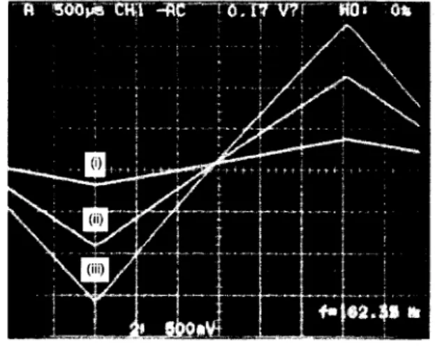
3V,
RL
= IOkW, C3 = 2C2 = 4Cl = 0.lpF and C4 = 0.44pF were used. Fig. 5 shows an oscilloscope photograph of the circuit with a 6Vp, triangular wave input. This photograph shows that the experimental circuit operates well as an attenuator without a deadband. The variable gain range of the circuit was -5.0dB to -20.5dB.Conclusion: A simple digitally programmable attenuator using FG-MOSFETs has been proposed. The device is very useful for analogue signal processing systenis.
0 IEE 2001
Electronic.7 Letters Online No: 20010416 D OI: IO. 1049/el:20OI0416
12 March 2001
K. Tanno, H. Tanaka, M. Syuto and 0. Ishizukd (Faculty of
Engineering, Miyaznki University, 1-1 Gakuenkitranadai-tiishi,
Miyuzuki-.rhi 889-2 192, Juprm)
E-mail: tanno@esl.miyazaki-u.ac.jp References
QIN, S., and G ~ I G E R , R.: 'A k5-V CMOS analog multiplier', ZEEE J.
Solid-State Circuits, 1987, SC-22, (6), pp. 1143-1 146
OTAKA, S . , TAiiIMOTO, H . , WATANABE. S., and M A E U A , 7.: 'A 1.9-GHz Si-bipolar variablc attcnuator for PHS transmitter', IEEE J , Solid-
Stute Circnit.y 1997, 32, (9); pp. 1424-1429
GRAY, P.R., and MEYER, R.G.: 'Analysis and design of analog integrated circuits' (John Wiley & Sons, 1993), 3rd cdn., Chap. 5
SHIHATA. T., and OHMI. T.: 'A functional MOS transistor featuring
gate-level weighted sum and threshold operation', IEEE Trans. Electron Devices, 1992, 39, (6), pp. 14441455
ZVT-PWM
boost converter for unity power
factor applications
C.C. Wu a n d C.M. Young
A ncw single-phase ZVT-PWM boost converter with an active snubber is proposed to achieve unity power factor operations for a wide load range. The unique location of the resonant inductor and capacitor ensures that low switching strcss and commutation losses are obtained in the converter. The proposed converter is suitable for high power factor correctors.
Intrurluctiun: In recent years, various soft-switching techniques have been proposed to reduce switchmg losses and EM1 noise in switching mode converters. The zero voltage transition-pulsewidth modulation (ZVT-PWM) converters introduced in [l, 21 have been the most successful. They combine desirable features of both the conventional PWM and the soft switching resonant technique.
Soft switching commutation is achieved in the main switch and, as a result, the power losses and EM1 are reduced considerably. However, the auxiliary switch in [I] is turned off with hard swtch- ing. In [2], the voltage across the auxiliary switch is higher than the output voltage. To overcome these disadvantages, a new sin- gle-phase ZVT-PWM boost converter is suggested in this Letter. This converter is able to lmprove on the disadvantages of the con- ventional ZVT-PWM boost convertcr [l, 21.
Db+ cb- Db-
+
D
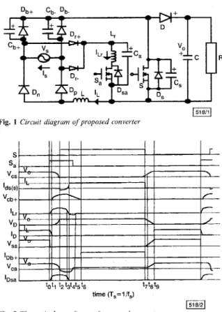
Fig. 1 Circuit diagram of proposed converter
1518121
Fig. 2 Theoretical wavejorms of proposed converter
Proposed converter': The main circuit topology is depicted in Fig. 1. The proposed converter is the combination of the conven- tional PWM boost converter and the active snubber resonant branch. When the input line is positive (or negative), (or Db +), 0,- (or Dr+) and
D,
(or Dp) are always turned off,Db+
(or Db ), Dp(or
DJ,
D,+
(or Dr-),D
and S perform the boost function with power factor correction. This converter differs from the conven- tional one. The changed location of the resonant inductor, capaci- tor and diode ensure low current and voltage stresses in the converter. In order to simplify the analysis, it is assumed that all the components are ideal (Cb+ = C, = C , > C,) and L is treated as a constant current source IL. For convenience in analysing the proposed converter, we will consider only the positive half-cycle of the input source. The circuit operation in one switching cycle can be divided into ten stages, and the key operating waveforms of the proposed converter are shown in Fig. 2.Stage (i) (to, t,): Prior to tu, S and So are off,
D
is conducting. At to, So is turned on in a zero current switching (ZCS) way andZLr(t) rises linearly from zero to I,. At t , ,
D
andDb+
are turned off with soft commutation.Stage (ii)
(z,,
fz): This is the resonant stage. The first resonant path is C,Cb+-O,+-L,S,-c,, and the second resonant path is Ca- L,-S,-C,. During this stage, C, and C, are discharged, and C,, is charged, then the growth rate of the voltage acrossD
is restricted by the voltage across C, to achieve zero voltage switching (ZVS) turn off. At t2, the voltage on S is zero, which is the end of this stage.Stage (iii) (t2, t3): This stage begins when S is tumed on at ZVS form. The resonance between L,, CO, and Cb+ continues through
Or+, Sa, and 0,. This stage finishes when ZLr(t) reaches I, again. Stage (iv) (t-,, t4): In this stage, the current in S,, f d s from I, to zero while the current in S rises from zero to ZL. This stage ends when ILr(t) is equal to zero.
Stage (v) (t4, ts): During this stage, C,, is linearly discharged by
I,
and the resonance between L,. and C, continues throughD,,,
Socan be turned off in a ZVS way. This stage fnishcs when ILr(t5) = 0.
Stage (vi) (ts, t6): During this stage, C,+ continues to linearly discharge by I,, through S. It finishes when the voltage on C,+ is zero.
Stage (vi) (16, t7): This stage begins when Db+ is tumed on in a ZVS way. The circuit operation is identical to the turn-on behav- iour of a conventional PWM boost converter.
Stage (viii) (t7, tx): This stage begins when S is turned off and eiids when VCx(t) is charged to Vcn(t5). During this stage, C, is charged linearly and the growth rate of the voltagc across S is lim- ited.
Stage (ix) (ts, t9): During this stage, C, and C, are charged line- arly by current
IL.
It finishes when Vcs(r) and V,.,d(t) is charged tov,
.
Stage (x) (t9, to): This stage begins when
D
is turned on under ZVS. The operation of the circuit at this stage is identical to the normal turn-off operation of a PWM boost circuit. Tt ends at thc moment that Sa is turned on to begin a new switching cycle.Based on the circuit analysis presented above, the proposed aclive snubber is activated only during the short ZVT transient; the ZVT-PWM converter is identical to a common PWM con- verter most of the time. Moreover, this converter can be easily built in conjunction with a power factor correction circuit.
a
Fig. 3 Measured u " x f h n s q/propo.~ed converter
N Experimental results of proposed converter Time: 1 pddiv
b Waveform of input line voltagc and linc currcnt Time: Siiisidiv
Experimentul results: A 250W prototype of the proposed con- verter was built and tested
(v,
= 120V,,,,,y,
= 250V, L, = 6pH, C,, = C,- = 22nF, C, = 2nF, C, = 2nF, L = 740pH, C = 680pF, f , = 100KHz). The key experimental results of the proposed con- verter are shown in Fig. LE. It can be seen that the experimental wavefoims are relatively clean and agree with the theoretical anal- ysis waveforms very well. The main switch is tumed on and turned off with ZVS. The auxiliary switch is tumed on with ZCS and turned off with ZVS. The conversion efficiency was found to be92y0 at the rated load. Fig. 3b shows the waveform of the input line voltage and line current. The input power factor is nearly unity.
Conclusions: A new ZVT-PWM boost converter using an active snubber has been proposed and tested. Its salient features are as follows: (i) soft switching operation can be eusily maintained for a wide line and load range; (ii) there are low switching stress and commutation losses in the converter, and (iii) the auxiliary snub- ber circuit is simple.
0 IEE 2001
Electronics Letters Online No: 20010427
DOI: 10.1049/el:20010427
C.C. Wu and C.M. Young (Department of Electvicol Engineering,
Ahtionul Taiwan University of Science und Technology, 43, Ktdung
Road, Sec. 4, Taipei, Taiwan 106, Republic o/' China)
E-mail: young@mouse.ee.iitust.edu.tw
12 Murclz 2001
References
1 HUA, ti., LIDU, c:.s., JIA"c,Y., and LEE, F.C.: 'Novel zero-voltagc-
transition PWM convcrtcr', IEEE Truns. Power Electron., 1994, 9, (2), pp. 213-219
YANG, L., and LEE, c.Q.: 'Analysis and design of boost zero voltage transition PWM converter'. IEEE Power Electron. Spcc. C o d Rec., 1993, pp. 707-713
2