1997 IEEE International Symposium on Circuits and Systems, June 9-1;?, 1997, Hong Kong
test or input reference --b
A LOW POWER HIGH ACCURACY CMOS TIME-TO-DIGITAL CONVERTER
-b -b . . .
Poki
Chen, Shen-Iuan Liu, and Jingshown
Wu
Department of Electrical Engineering, National Taiwan University, Taipei, Taiwan
ChinaABSTRACT actly in the last delay element. In the measurement, the
input period T,,, with TIl<Tref will be fed into the delay In this paper, we present a new CMOS time-to- line instead. Suppose that T,, disappears in the n-th delay digital converter (TDC) with the cyclic delay line struc- element, then the width is measured as n x TrCf / N ,
ture. The static supply current is 2-nA only. Furthermore, where N i:s the number of elements in the delay line. For the continuous calibration is no longer needed. The TDC a 20 M H ~ reference clock and a delav line of 64 can be shunt down between measurements to make the
power consumption negligible. The circuit with 64-stage cyclic delay line has been fitted into 0.25" x 0.75" chip area with a typical 0.8-pn SPDM process. The measured resolution is 286 picoseconds, and the meas- ured single-shot accuracy is less than 143 picoseconds. Both can be made much less if the control voltage is well tuned.
1. INTRODUCTION
Time interval digitization is an important building block for many instrumentation circuits, such as range finder, phase meter, robot vision, PM demodulator, etc.[l-31 Due to its large power consumption and circuit size, the conventional TDC with subnanosecond resolu- tion can hardly be implemented in the portable sys-
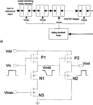
tems[4]. At the end of 1995, a novel TDC circuit, named linear TDC here due to its linear delay line structure, is proposed to get 780 picoseconds resolution (after aver- aging hundreds of measurements) with 15 mW power consumption[5]. The portability problem is thus solved at the expense of 3ns single shot accuracy. Figs. l a and 1 b show the block diagrams of the circuit and the pulse- shrinking delay element.
Basically, the pulse-shrinking delay element is a sig- nal buffer composed by two NOT gates. The maximum conductible current of the first NOT gate is controlled by the bias voltage Vbias. The degree of width shrinking of the input pulse can be easily controlled through ad- justing Vbim. A reference pulse with duration Tref is fed into the delay line for calibration. The delay-locked loop, cooperating with another delay line of same size, will adjust Vbias to make the reference period disappear ex-
ments, the resolution is 50 ns/64=780 p s theoretically.
Dulse-shrinkina I V b l a s I I
I
delay44;ked, c J
I=+
(b)Fig. l a The block diagram of the linear TDC
l b 'The pulse-shrinking delay element
This circuit established a milestone of low-cost, high-accuracy portable TDC systems. But there are still some important features needed to be improved. Due to many unavoidable variations [5,6], the calibration of the TDC must be done continuously to keep Treyjust disap- pear in the last element of the delay line. This consumes much system power, and the circuit can not be shunt down between measurements for power savings, Also,
the mismatch among pulse-shrinking delay elements results in poor delay line linearity. This sets a serious limit to the TDC resolution. When higher TDC resolu- tions are required, the pulse-shrinking delay line must be lengthened to accommodate more delay stages. And the linear TDC will become too long and must be folded into 2 or more segments due to reasonable chip width or length limit. The inter-segment wiring is much longer than the intra-segment one[6]. It causes large non- linearity error and further limits the resolution of the TDC to be 6- to 7-bits only.
Finally, the input pulse shrink more rapidly at the last few elements, because it will become too short to drive the next stage to toggle its state. For the TDCs with coarse resolution, this phenomenon may not be noticeable. But for the TDCs with deep sub-nanosecond resolution, this kind of nonlinearity will dominate and deteriorate the accuracy. To overcome all these prob- lems, a new TDC circuit is proposed in this paper. The circuit has been implemented by a 0.8-pm SPDM CMOS process.
2. OPERATION PRINCIPLES
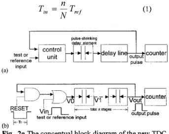
The block diagram of the new TDC is shown in Fig. 2a. The input pulse circulates in the cyclic structure. It shrinks a certain amount in each cycle until it thor- oughly diminished. Assume that the counter counts N for the reference input Tref and n for the test interval T,,,,
then T,,, is measured as:
(1)
I
Dulse-shrinkinaI
counter unit test or input (a) output pulseU
test or reference input @) t-Tr--Fig. 2a The conceptual block diagram of the new TDC 2b The circuit of the new TDC in Fig. 2a
Practically, the pulse-shrinking delay elements can also served as delay units. So, the ideal delay line in Fig. 2a is replaced by series-connected pulse-shrinking delay
elements as shown in Fig. 2b. Since the whole circuit of the new TDC is equivalently composed by even number of NOT gates, there are two stable states, V,=V,
-
* *=V,,,= LOW and V,=V, 1.
*=V,,,=HIGH.Where V, is the output of the i-th element in the delay line. To make sure that the circuit settles in the proper stable state V,=V,
-
* .=V,,,=LOW from power on, anexternal control pin RESET must be added as shown in Fig. 2b. The degree of shrinking is controlled by the bias voltage Vbla which can be adjusted to get over 10' or much more cycles for the reference period Trcf The cor- responding resolution can be extremely fine.
Because the element mismatch and intra-segment wiring mismatch discussed will be went through per cycle by the input pulse, there will not be any measure- ment nonlinearity from cycle to cycle. The linearity problem is solved successfully. In this new TDC, it is not necessary to keep the reference pulse Trc,just disap- peared at some specific cycle or stage. Only if the bias voltage V,,, is properly adjusted such that Trey circulates the delay line enough times before diminished out to keep sufficient resolution. The continuous calibration is no longer needed, and the circuit can be shunt down between measurements to save power. Also, the associ- ate delay-locked loop and its cooperating delay line can be saved. This greatly simplify the TDC circuit.
Basically, the output bits of the new TDC are unlim- ited. It can be increased by merely adding the number bits of the internal counter in Fig. 2b. And the control of
vb,, must be made accurate enough. On the contrast, the
linear TDC[10] must double the size of its delay lines to increase merely one output bit. No averaging is needed to improve the resolution. Because the single-shot reso- lution itself is accurate enough. The nonlinearity, caused by the pulse shrinking out more rapidly at the last few stages, can be treated as a constant count offset for a given bias voltage Vbla. And it can be completely cali- brated out by the following technique.
Offset Elimination: First, feed T,, and Tre/2 into the TDC input. Assume that the circuit gets N and N' counts respectively. Then
and
v
(3)
Where a is the effective resolution, and T,,fl,cr is the measurement offset caused by faster shrinking just be- fore the input pulse disappeared.
L f
2(
N
-N ' )
a
=
(4)If the calculated resolution a is above requirement, we must raise Vbias carefully to make N large enough. This in turn lowers the effective resolution a to a satisfactory value as expected from eq. (4). Next, feed measured
interval
TI,
into the TDC input, and assume that the counter result is n. Then, the measured width of T,,, be- comes:3. EXPERIMENTAL RESULTS
To demonstrate the feasibility of the proposed TDC, we have fabricated the circuit with a 0 . 8 - p SPDM CMOS process. The new TDC is composed by 64 delay elements with ( W / L ) = ~ ~ ~ / O . S , U ~ for P1 and N1 transis- tors, (W/L)=7.6,~m/0.8p for P2 transistor, (W/L)=2.3 p / 0 . 8 p for N2 transistor, and ( W / L ) = 1 . 3 p / O . 8 p for N3 transistor in each pulse shrinking delay element. The photomicrograph of the new TDC is shown in Fig.
3. The size of circuit is reduced to 0.14 mm x 0.75 mm
(without the internal counter). If the internal counter is included also, the chip size is estimated to be 0.25" x
0.75 mm. All the experimental results presented here are collected from these prototype chips. The static dissipa- tion current is less than 2 nA, and the average current consumption is calculated to be less than 100 nA from a 5-
v
supply.Fig. 3 The photomicrograph of the new TDC
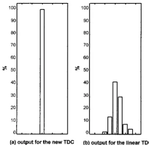
Fig. 4a shows a typical output code distribution for 50 single-shot measurements of the new TDC. Com- pared with Fig. 4b, the typical distribution of single-shot measurements of the linear TDC[5], the single-shot measurement of the new TDC is very stable. No averag- ing is needed to improve the resolution. To explore the
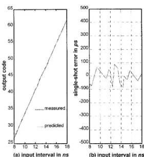
effective resolution and the measurement offset of the new TDC, a series of experiments with the same condi- tion were conducted. The only parameter varied was the width of the input pulses generated by HP 81 10A pulse generator. The same input pulse widths were also meas- ured with a Standford Research Systems SR620 univer- sal counter. The measured results of single-shots along with the theoretical prediction line are depicted in Fig. 5a. It shows that the experimental data agrees with the prediction. From eq. (2), the effective resolution cx is calculated to be 286 ps. Also, the measurement offset
rfl,,,
is calculated to be 344 ps. This again confirmsour inference that the input pulses shrink faster just be- fore diminished. The dead time of single-shot measure- ments is at most a few microseconds. The measurement rate of at least lOOkHz is promised. Fig. 5b shows the error between single-shot measurements and the theo- retical calculation. All the errors are below 1/2 resolu- tion (143 ps). This assures every output bit is valid.
d,
(a) output for the new TDC (b) output for the linear TDC
Fig. 4 Typical distribution of single-shot measurement results in 50 measurements for (a) the new TDC, (b) the linear TDC
The effective resolution and the single-shot accuracy can be further improved, if we control the bias voltage
Vbiar more accurately. By simulations, the resolution of the new TDC can be as low as tens of picoseconds or less. Table I shows a portion of simulation result for
Vbias = 3.10 V and
Ti,,
= 6.011s. The effective resolution is about 37.5 p s .ACKNOWLEDGMENT , , shrinkage@) 500 , , , , / ‘ / I 37.4 37.6 37.5 37.5 6 7 8 9 10 5.7884 5.7509 5.7135 5.6759 5.6385
(a) input interval i n n s (b) input interval in ns
Fig. Sa The result of the single-shot measurements and the theoretical prediction line
5b The measured single-shot error
Table. I The beginning portion of the simulation
result with Vbi,=3.lOV, T,,,=6 ns.
pulse no. 1 1 1 2 1 3 1 4 1 5
width(ns) 15.9758 15.9384 15.9008 15.8633 15.8258
I
7.4 137.5 137.4 137.6 137.4
4. SUMMERY
An extremely low-power and high-accuracy CMOS time-to-digital converter with the cyclic delay line struc- ture has been presented. With the 0.8-,um SPDM process and 64 delay elements, this new TDC can measure input interval up to 20 ns and reach a resolution of 286 ps
experimentally. The measured single-shot accuracy is less than 112 resolution. No averaging is needed to im- prove accuracy. The TDC induces almost no extra cost for increasing the number of its output bits. When coop- erated with TDCs using counter method, this TDCs can be used as interpolation circuits[7] to greatly increase the linear measurement range while keeping the same resolution. No continuous calibration is needed. This enables the TDC to be shunt down between measure- ments to save more battery power. This certainly opens another possible applications of the new TDC in low power and portable systems.
The authors would like to express their deep appre- ciation to Miin-Hwa Jiang of Center for Measurement Standards, Industrial Technology Research Institute for his measurement advising and instruments providing. The authors would like also to thank the National Sci- ence Council for financial supporting and thank the Chip Implementation Center (CIC), National Science Council, Taiwan, for the fabrication of the test chip. This work was sponsored by NSC-85-2622-E-002-010.
REFERENCES
Maatta, J. Kostamovaara , M. Koskinen, and R. Myllyla, “Time-to-digital converter for fast, accu- rate laser range finding,” in Proc. SPIE Industrial
Inspection, Sept. 1988, vol. 1010, pp. 60-67.
J. Kostamovaara, K. Maatta, M. Koskinen, and R.
Myllyla, “Pulsed laser radars with high- modulation-frequency in industrial applications,” in Proc. SPIE Laser Radar VU: Advanced Technol.
Applicant., Jan. 1992, vol. 1633, pp.114-127
Rapeli et al. “Method and circuitry for demodula- tion of angle modulated signals by measuring cycle time, ” US Patent 5,2 70,666, Dec. 1993.
T. Otsuji, “A picosecond-accuracy, 700-Mhz range si-bipolar time interval counter LSI,” ZEEE J. Solid-state Circuits, vol. 28, pp.941-947, Sept.
1993.
Elvi Raisanen-Ruotsalainen, etc. “A Low-Power CMOS Time-to-Digital Converter,” IEEE JSSC,
vol. 30, No. 9, pp. 984-990, Sept. 1995.
Timo E. Rahkonen, etc. “The Use of Stabilized CMOS Delay Lines for the Digitization of Short Time Intervals,” ZEEE JSSC, vol. 28, No. 8, pp.
R. Nutt, “Digital time intervalometer,” Rev. Sci.
Instrum., vol. 39, no. 9, pp. 1342-1345, 1968.
887-894, Aug. 1993.