行政院國家科學委員會補助專題研究計畫成果報告
※※※※※※※※※※※※※※※※※※※※※※※※※
※
※
※ 具有新式副閘極結構的低溫複晶矽薄膜電晶體
※
※
的 製 作 與 分 析 ※
※
※
※※※※※※※※※※※※※※※※※※※※※※※※※
計畫類別:■個別型計畫
□整合型計畫
計畫編號:NSC89-2215-E-009-104
執行期間:89 年 08 月 01 日至 90 年 07 月 31 日
計畫主持人:黃調元博士
協同研究人員: 林鴻志博士
本成果報告包括以下應繳交之附件:
□赴國外出差或研習心得報告一份
□赴大陸地區出差或研習心得報告一份
■出席國際學術會議心得報告及發表之論文各一份
□國際合作研究計畫國外研究報告書一份
執行單位:國立交通大學電子工程學系
中 華 民 國 90 年 10 月 31 日具有新式副閘極結構的低溫複晶矽薄膜電晶體的製作與分析
Fabr ication and Char acter ization of Low-Temper atur e Polysilicon Thin Film
Tr ansistor s with Novel Self-Aligned Sub-Gate Str uctur es
計畫編號:NSC89-2215-E009-104 執行期限:89 年 8 月 1 日至 90 年 7 月 31 日 主持人: 黃調元 國立交通大學電子工程學系 共同主持人:林鴻志 國科會國家豪微米元件實驗室
中文摘要
具有電場感應源/汲極(FID)結構的新 式複晶矽薄膜電晶體,可有效降低傳統結 構中的由於高電場所造成的汲極漏電流, 提昇開關電流比。而經由變溫及結構上的 分析可以更清楚得知此新式結構的優點。摘要
Characteristics of poly-Si thin-film transistors with source/drain extensions induced by a bottom sub-gate were explored. Nevertheless, the performance is significantly degraded by a drastic increase of off-state leakage current when the channel length is scaled below 1 µm. Moreover, a hump in subthreshold current-voltage regime is observed. After careful analysis, it is found that the leakage current is strongly dependent on the field strength and is not a thermally activated process. A leakage path along the bottom interface of the poly-Si channel layer is proposed to explain these results.
緣由與目的
Polycrystalline silicon (poly-Si) thin-film transistors (TFTs) have been used in a wide variety of applications. However, a large off-state leakage current normally
encountered in poly-Si TFTs fabricated with self-aligned source/drain structure represents one of the key limitations for many practical applications.1) We have recently proposed a new FID structure with a bottom sub-gate.3) Such a new structure would make the manufacturing process more flexible. Nevertheless, detailed characterization on the bottom sub-gate devices, especially the leakage characteristics and their dependence on the channel length, are still lacking. This study was therefore carried out to explore these issues by fabricating and characterizing both n- and p-channel TFTs with bottom sub-gate.
實驗過程
Figure1 shows cross-sectional and top views of a FID TFT with bottom sub-gate. The device’s channel length, L, is thus defined by the spacing between the two branches of the sub-gate. First, a 100-nm n+-poly-Si layer was patterned to form the fork-shaped bottom sub-gate. Next, a 100-nm CVD nitride layer was deposited, followed by the deposition of a LPTEOS
(550 nm) oxide layer. Chemical mechanical polishing (CMP) was then applied to planarize the wafer surface and to expose the nitride layer on top of the sub-gate. Afterwards, a 50-nm CVD amorphous Si film was deposited at 550 ℃ , and subsequently transformed into polycrystalline phase by a solid-phase crystallization (SPC) treatment at 600 ℃ for 24 hours to serve as the active device layer. A 20-nm CVD oxide layer was then deposited to form the gate insulator. An n+ poly-Si film was deposited and patterned to form the top main-gate. Next, the offset source/drain regions were defined by a photoresist step that was used for masking the source/drain ion implantation. Wafers then followed a standard back-end processing to form the contact pads, and received a plasma treatment at 250℃ in NH3 ambient for 3 hours before
measurements.
結果與討論
Figures 2 (a) and (b) show the effect of sub-gate bias on the n- and p-channel device operations, respectively. It can be seen that, even with a proper main-gate voltage, the new TFT cannot be effectively turned on when the sub-gate bias is zero. This is simply because the field-induced drain and source extensions are not formed. When a high sub-gate bias with proper polarity is applied, both on and off currents could be
improved, resulting in good transfer behavior.
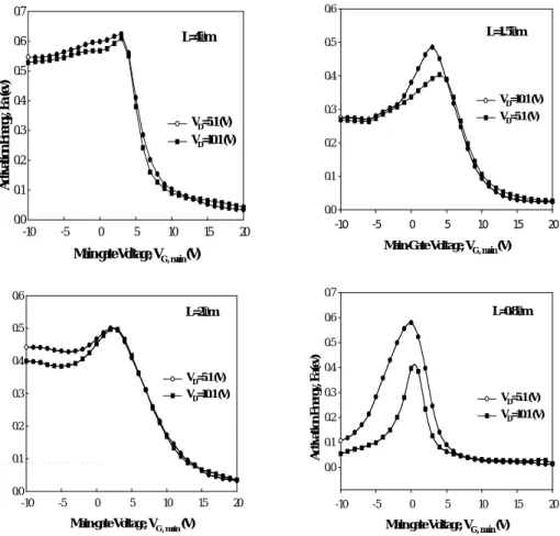
Figures 3 (a) and (b) show the effect of channel length on the subthreshold characteristics of n-channel and p-channel devices, respectively, with a drain voltage of 10.1V. One interesting phenomenon shown in Figs. 3 (a) and (b) is the appearance of a “hump” in the subthreshold region as L is scaled down or as drain bias increases. This finding implies that some kind of leakage path with a lower turn-on threshold is formed during device operation. In order to clarify the leakage current mechanism, the temperature dependence of the drain current was investigated. Figures 4(a) ~ (d) show the extracted activation energy, EA, as a
function of gate bias for n-channel devices with L of 4, 2, 1.5, and 0.8 µm, respectively. Though the results for p-channel operation are not shown, similar trend was observed. When L is long (e.g., 4 µm), EA is roughly
equal to 1/2 bandgap (Eg) of Si (0.56 eV), and shows only very weak dependence on both the gate and drain biases in the off-state region. This indicates that generation-recombination of carriers via the mid-gap grain boundary traps is probably the dominant leakage mechanism, similar to that observed in previous report .2)
When L becomes shorter, however, EA
becomes more sensitive to both gate and drain voltages. This is seen in Figs. 4(b) ~ (d)
where EA decreases with increasing drain
bias or decreasing gate bias (in the negative Vg regime). When L is scaled to 0.8 µm, EA
could even be lower than 0.1 eV at Vd of 10.1 V and Vg <-5V. This indicates that the involved leakage mechanism is not a thermally activated process, and is strongly dependent on the field strength.
Based on the above analysis, the additional leakage path for the short-channel devices is believed to be through the bottom interface of the active layer, as is schematically illustrated in Fig.5. In this figure, the main-gate voltage is much smaller than the threshold voltage, thus essentially no free carriers (i.e., electrons in the n-channel case) are induced in the channel underneath the main-gate. However, the carriers in the induced source extension region would be attracted by the drain field and thus contribute to the leakage if the channel length is short enough or if the drain voltage is high enough. As a result, a hump in subthreshold I-V regime would occur.
結論
In this work, TFT devices with electrical source/drain extensions induced by a bottom sub-gate were characterized. Nevertheless, an anomalously high off-state leakage current is observed in devices with shorter channel, which results in a hump in the subthreshold I-V regime. The leakage is very sensitive to the drain bias with a low thermal activation energy. It is believed that
the leakage path is mainly through the bottom interface of the poly-Si active layer.
參考資料
[1] J. G. Fossum, A. Ortiz-Conde, H. Shicjijo, and S. K. Banerjee: IEEE Trans. Electron Devices 32 (1985) p.1878.
[2] K. Tanaka, K. Nakazawa, S. Suyama, and K. Kato: IEEE Trans. Electron. Devices 39, (1992) p.916.
[3] H. C. Lin, M. Yu, C. Y. Lin, K. L. Yeh, T. Y. Huang, and T. F Lei: IEEE Electron Device Lett. 22 (2001) p.26.
Main gate Voltage, VG , main (V) -10 -5 0 5 10 15 20 A ct iv at io n E ne rg y, E a( ev ) 0.0 0.1 0.2 0.3 0.4 0.5 0.6 0.7 VD=5.1 (V) VD=10.1 (V) L=0.8µm Main-Gate Voltage, VG , main (V)
-10 -5 0 5 10 15 20 A ctivation E nergy, E a(ev) 0.0 0.1 0.2 0.3 0.4 0.5 0.6 VD=10.1 (V) VD=5.1 (V) L=1.5µm VD=10.1(V)
Main-Gate Voltage, VG , main (V)
-5 0 5 10 15 20 D r a in C u r r e n t, I D (A ) 10-12 10-11 10-10 10-9 10-8 10-7 10-6 10-5 10-4 10-3 L=4µm L=3µm L=2µm L=1.5µm L=1µm L=0.8µm Main-gate Sub-gate Drain Sour ce L = 0.8 ~ 4 µm Off-set length = 1 µm Oxide Nitride Substrate Top main-gate
Bottom sub-gate Poly-Si channel layer
L= 3 µm VD= 15.1 (V)
Main-gate Voltage, VG , main (V)
-5 0 5 10 15 20 D ra in C ur re nt , I D (A ) 10-11 10-10 10-9 10-8 10-7 10-6 10-5 10-4 VG ,su= 0 (V) b VG ,su= 40 (V) b L= 3 µm VD= -15.1 (V)
Main-gate Voltage, VG , main (V)
-20 -15 -10 -5 0 5 D ra in C ur re nt , I D (A ) 10-13 10-12 10-11 10-10 10-9 10-8 10-7 10-6 10-5 10-4 10-3 VG ,su= 0 (V) b VG , sub= -40 (V) VD= -10.1(V)
Main-Gate Voltage, VG , main (V) -20 -15 -10 -5 0 5 D r a in C u r r e n t, I D ( A ) 10-12 10-11 10-10 10-9 10-8 10-7 10-6 10-5 10-4 10-3 L=4µm L=3µm L=2µm L=1.5µm L=1µm L=0.8µm Sub-gate Sub-gate n+ n + Main-gate Gate Oxide Dr ain Sour ce
Fig. 1 Cross-sectional (a) and top (b) views of the TFT device with bottom sub-gate.
Fig. 2 Effects of sub-gate bias on the transfer characteristics for (a) n-channel and (b) p-channel devices.
L=4µm
Main-gate Voltage, VG , main (V)
-10 -5 0 5 10 15 20 A ct iv at io n E ne rg y, E a (e v) 0.0 0.1 0.2 0.3 0.4 0.5 0.6 0.7 VD=5.1 (V) VD=10.1 (V) L=2µm
Main-gate Voltage, VG , main (V)
-10 -5 0 5 10 15 20 A ctivation Energy, Ea(ev) 0.0 0.1 0.2 0.3 0.4 0.5 0.6 VD=5.1 (V) VD=10.1 (V)
Fig. 3 Subthreshold characteristics of (a) n-channel and (b) p-channel TFT devices with various channel length at VD=10.1V. Sub-gate bias is 40 V.
Fig.4 Extracted activation energy as a function of main-gate and drain voltages for n-channel TFT devices with L = (a) 4 μm, (b) 2 μm, (c) 1.5 μm, and (d) 0.8 μm. Sub-gate bias is 40 V.
Fig. 5 Illustration of an additional leakage path along the bottom interface of the poly-Si active layer.