國立交通大學
電子工程學系 電子研究所碩士班
碩 士 論 文
修正蕭基位障非揮發性記憶體於薄膜電晶體基
板之研究
A Study on Non-volatile Memory with Modified
Schottky Barrier S/D on TFT Substrate
研 究 生:賴瑞堯
指導教授:崔秉鉞 教授
修正蕭基位障非揮發性記憶體於薄膜電晶體基
板之研究
A Study on Non-volatile Memory with Modified
Schottky Barrier S/D on TFT Substrate
研究生:賴瑞堯 Student: Jui-Yao Lai
指導教授:崔秉鉞 Advisor: Bing-Yue Tsui
國立交通大學
電子工程學系 電子研究所
碩士論文
A thesis
Submitted to Department of Electronics Engineering & Institute of Electronics
College of Electrical and Computer Engineering
National Chiao Tung University
in Partial Fulfillment of the Requirement
for the Degree of Master
in
Electronic Engineering
2010
Hsinchu, Taiwan, Republic of China
修正蕭基位障非揮發性記憶體於薄膜電晶體基
板之研究
研究生: 賴瑞堯 指導教授: 崔秉鉞
國立交通大學電子工程系 電子研究所碩士班
摘要
在本論文中,我們對於薄膜電晶體基板上具有修正蕭基位障源極/汲極之快 閃記憶體進行研究。實驗試片之閘極薄膜層採用 SONOS 搭配 p 型複晶矽閘極。其 源極/汲極分為純蕭基位障、修正蕭基位障、和傳統 P-N 接面。我們將探討不同 源極/汲極結構對其記憶體特性的影響。 在 Fowler-Nordheim 寫入機制中,修正蕭基位障源極/汲極記憶體相對於其 他結構展現較佳的寫入速度。因此,修正蕭基位障除具有低溫製程之優點,在寫 入速度上亦具有其競爭力。在通道熱電子(channel hot electron)寫入機制中, 修正蕭基位障記憶體元件為汲極端注入特性。未達成源極端注入造成修正蕭基位 障源極/汲極記憶體有較差之寫入速度。純蕭基位障源極/汲極可達成源極端注 入,但其原因乃從源極進入之電子較少,使得無法有大量源極端注入效果發生。 總體來說,修正蕭基位障源極/汲極記憶體之寫入速度特性未有突破性攀升,原 因 為 電 子 在 被 陡 峭 蕭 基 位 障 能 帶 加 速 時 遭 到 通 道 中 複 晶 矽 之 晶 界 (grain boundaries)干擾,使熱電子較難產生。通道熱電子寫入之後,帶對帶熱電洞(band-to-band hot hole)抹除機制只有在 傳統 P-N 接面源極/汲極有明顯抹除效果。複晶矽通道上薄穿隧氧化層之品質導 致本論文中記憶體元件在儲存資料持有性上之表現較差。多次寫入/抹除之後, SONOS 結構會發生抹除困難(hard-to-erase)之現象。104 次寫入/抹除之後,試 片普遍開始性能退化。以 Fowler-Nordheim 寫入時,修正蕭基位障源極/汲極記 憶體元件由於會產生能量較高的電子,且儲存位置較集中於靠近源極/汲極的位 置,因而相較之下其性能退化較嚴重。以通道熱電子寫入時,傳統 P-N 接面源極 /汲極會集中於汲極端產生高能量高的電子注入,因而其性能退化較嚴重。
A study on non-volatile Memory with modified
Schottky Barrier S/D on TFT substrate
Student: Jui-Yao Lai Advisor: Bing-Yue Tsui
Department of Electronics Engineering
Institute of Electronics
National Chiao Tung University
Abstract
In this thesis, flash memory on thin film transistor (TFT) substrate with source/drain (S/D) engineering by the formation of implant to silicide (ITS) modified Schottky-Barrier (MSB) is studied. The gate stack of experiment samples are set to be SONOS with p-type poly silicon gate. S/D formation is verified into pure Schottky-Barrier (SB), MSB, and conventional p-n junction. Memory characteristics of the cells with different S/D structure are investigated both in Fowler-Nordheim (FN) and channel hot electron (CHE) programming.
In FN programming, MSB S/D memory exhibits slightly better program speed than conventional S/D. Therefore, the MSB S/D shows the competitiveness since it can be formed by low thermal budget and less time consumption fabrication process. In CHE programming, MSB S/D memory has drain side injection. That the source side injection is absent leads to poor CHE program speed for MSB S/D. Pure SB S/D has the fewer supply of electrons from source so it results in weak source side injection which isn’t helpful to program efficiency. In general, the speed improvement
banding could accelerate electrons. The reason is that the hot electrons become more difficult to be generated since the grain boundaries in poly silicon channel disturb the acceleration of sharp SB band bending.
It is found that the efficiency of FN erasing isn’t affected by S/D engineering. After CHE program, band-to-band hot-hole (BBHH) shows the erase ability only in conventional S/D. In this thesis, the poor quality of thin tunneling oxide on poly-silicon grain causes poor 10-year extrapolated charge retention. Hard-to-erase phenomenon happens in endurance characteristic since the deep level trapping in SONOS nitride layer. The memory window loss relates to the uniformity of charge storage, the generation of interface states, and the energy of election injection. In FN programming endurance characteristic, swing degradation for MSB S/D memory is larger than for conventional S/D, due to its higher injection energy. On the other hand, in CHE programming endurance characteristic, conventional S/D memory has more serous swing degradation than MSB S/D since it has local and large amount of hot electron injection at drain side.
誌謝
碩士歷程終於告一段落,在邁向下一個人生進程的同時,我滿載著知識和回 憶。修課、規畫、實驗、量測、分析、撰寫論文、準備口試、完善論文,碩士的 每一階段、每一步驟皆讓我學到很多和成長很多。在此,我要感謝在這之中幫助 過我的人、鼓勵過我的人。 首先感謝我的指導教授 崔秉鉞老師,老師從我大學專題就一直指導到我做 出碩士論文。從老師身上,我學到非常多,包括滿滿的專業知識,很多處事的態 度。感謝老師,在我研究出現問題時,費時費心地和我討論,在我碰到困境時, 不斷地給予我鼓勵。由於老師的指導讓我有正向的人生和研究的觀念,讓研究的 一切得以在最終有好的結果。 感謝實驗室博士班的學長:謝志民、盧季霈、李振銘。感謝他們,在我實驗 規畫和試片製作上的細節給的幫助,在實驗分析和論文撰寫上把他們的知識和經 驗和我分享。感謝吳明錡、李振欽和羅正愷學長以及劉筱函和張孝瑜學姊,與我 討論一些研究上遇到的問題。感謝實驗室同屆的王俊凱、余昆武、蔡依成和我一 起學習機台,一起共渡實驗的甘苦。感謝學弟勃學、子歆、志展讓在實驗室的陪 伴。 感謝交通大學奈米中心和國家奈米實驗室在我研究的實驗部分所給予的協 助。感謝蕭逸璿學長,蘇彬老師實驗室的吳育昇、范銘隆和郭俊延學長,在元件 模擬上給過的一些建言和幫助。感謝陪伴我的女朋友鐘雅琪,感謝她的照顧和給 我很多信心和勉勵。 最後,感謝我的爸媽:賴俊文和宋秀真,他們在我碩士和整個人生裡一直扮 演最重要的角色,對於我總是給予支持和鼓勵,勉勵我上進並且照顧我的生活。 感謝在彰化員林的家,讓我在身心疲憊的時候,可以回去充電。感謝我慈祥的奶Contents
Abstract (Chinese)………I
Abstract (English) ……….III
Acknowledge (Chinese)………...V
Contents………..VI
Table Captions……….VIII
Figure Captions………...IX
Chapter 1 Introduction……….1
1-1 Non-volatile flash memory……….….1
1-1-1 Thin film transistor (TFT) memory device………...1
1-1-2 TFT non-planar and nano-wire memory…..………....….2
1-1-3 Implant to silicide (ITS) technique on TFT..………3
1-2 Engineering for TFT memory device……...………..4
1-2-1 Gate engineering……….………..5
1-2-2 Source/Drain engineering by modified Schottky-Barrier (MSB).7 1-3 Motivation and thesis organization………8
Chapter 2 Experimental procedure………...15
2-1 Device fabrication………..15
2-1-1 TFT sample……….16
2-2 Electrical Characterization Techniques………...18
2-2-1 Read operation………18
2-2-3 Retention………...…..19
2-2-4 Endurance………...…………19
Chapter 3 Characteristics of the Thin Film Transistor (TFT)
Memory device………26
3-1 Introduction……….………..26
3-2 Device structure Inspection………..27
3-3 Sample definition and basic I-V characteristic………...27
3-4 Memory characteristic of Fowler-Nordheim program………...29
3-4-1 I-V characteristic and memory window……….29
3-4-2 Program/Erase speed………..29
3-4-3 Retention and endurance………32
3-5 Memory characteristic of Channel Hot Electron program…………33
3-5-1 Basic I-V characteristic and Memory window………...33
3-5-2 Program/Erase speed………..35
3-5-3 Retention and endurance………38
3-6 Summary……….39
Chapter 4 Conclusions and Future works……….…76
4-1 Conclusions……….…76
4-2 Future works………..78
Table Captions
Chapter 2
Figure Captions
Chapter 1
Fig. 1-1: Schematic of Vertical Gate NAND array………..10 Fig. 1-2: Schematic of Vertical Cell NAND array………...10 Fig. 1-3: Stress Induced Leakage Current (SILC) in floating gate (FG) non-volatile
memory………...11 Fig. 1-4: Discrete Charge Storage in SONOS non-volatile memory………..11 Fig. 1-5: Program/Erase band diagrams of (a) SONOS, and (b) MANOS………….12 Fig. 1-6: Band-gap Engineering………..…13 Fig. 1-7: Modifications of conventional floating gate structure………...14
Chapter 2
Fig. 2-1: Memory device with MSB S/D on TFT………...22 Fig. 2-2: Process flow of MSB TFT SONOS non-volatile memory. (a) isolation and
channel film preparation, (b) gate stack formation, (c) spacer formation, (d) NiSi formation, (e) MSB formation, (f) Conventional S/D formation…...23
Chapter 3
Fig. 3-1: TEM images of sample M30; (a) Overview; (b) view of S/D side………..41 Fig. 3-2: The basic I-V curves of all the samples...………42 Fig. 3-3: The memory window of each sample. (a) sample CON; (b) sample M30; (c)
sample M10; (d) sample M01; (e) sample PSB………...43 Fig. 3-4: The FN program speed of each sample. (a) sample CON; (b) sample M30;
Fig. 3-5: The comparison of FN program speed between samples with different S/D formation………..48 Fig. 3-6: The comparison of FN program Vth shift under same pulse width between
samples with different S/D formation………….……….48 Fig. 3-7: S/D structure of the samples: (a) sample PSB; (b) sample M01.………….49 Fig. 3-8: The sharp band causes higher injection in MSB S/D. (a) ideal case; (b) on
TFT substrate………49 Fig. 3-9: The comparison of FN erase in the pulse of Vg = -18V for 1ms…….…….50 Fig. 3-10: The FN erase speed of each sample. (a) sample CON; (b) sample M30; (c)
sample M10; (d) sample M01……….….51 Fig. 3-11: The large window retention of each sample. (a) sample CON; (b) sample
M30; (c) sample M10; (d) sample M01………..….53 Fig. 3-12: The millisecond cycle retention of each sample. (a) sample CON; (b)
sample M30; (c) sample M10; (d) sample M01………..55 Fig. 3-13: The endurance of FN programming for each sample. (a) sample CON; (b)
sample M30; (c) sample M10; (d) sample M01………..57 Fig. 3-14:I-V degradation after 104 FN P/E cycles of each sample (a) sample CON; (b)
sample M30; (c) sample M10; (d) sample M01...59 Fig. 3-15: Band diagram of drain side electron effect on read operation for
conventional p-n S/D. (a) off-current increases in forward read; (b) Vth shift goes further in reverse read………..61 Fig. 3-16: I-V curves of CHE programming with forward and reverse read (a) sample
CON; (b) sample PSB; (c) sample M30; (d) sample M10; (e) sample M01...………...61 Fig. 3-17: Channel hot electron (CHE) program speed for each sample (a) sample
Fig. 3-18: Comparison of channel hot electron (CHE) program speed………66 Fig. 3-19: Band diagram of CHE injection in MSB device (a) ideal case (b) on TFT..66 Fig. 3-20: The comparison FN erase after CHE program……….67 Fig. 3-21: The comparison BBHH erase after CHE program………...67 Fig. 3-22: The Id-Vg curve after BBHH erase: (a) sample M10; (b) sample
M01………..………68 Fig. 3-23: The erase speed after CHE program. (a) sample CON; (b) sample M30; (c)
sample M10; (d) sample M01………..69 Fig. 3-24: The retention of CHE program. (a) sample CON; (b) sample M30; (c)
sample M10; (d) sample M01………..71 Fig. 3-25: The endurance of CHE program. (a) sample CON; (b) sample M30; (c)
sample M10; (d) sample M01………..………73 Fig. 3-26: I-V degradation after 104 P(CHE)/E(FN) cycles of (a) sample CON; (b)
sample M30...75
Chapter 4
Fig. 4-1: I-V curve of P/E state just after 105 P(FN)/E(FN) cycles and 3 months later...80 Fig. 4-2: I-V curve of P/E state just after 105 P(CHE)/E(FN) cycles and 3 months
Chapter 1
Introduction
1-1 Non-volatile flash memory
Since the first floating gate non-volatile memory was invented by D. Kahng and S. M Sze at Bell Labs in 1967 [1], flash memory has developed into a huge necessary requirement both in electronic industry and people’s daily life. The applications of flash memory spanned widely in electronic area, especially in portable devices such as PDA, cell phone, digital camera, or music player. The low power consumption property, non-volatile characteristic, electrical program/erase operation, and CMOS compatible process technique are its advantages. They all make non-volatile flash memory irreplaceable.
1-1-1 Thin film transistor (TFT) memory device
Nowadays, semiconductor industry has encountered a scale down and cost down age, which means the denser circuits we can make the more benefits we can get. Flash memory is very widely used in electronic devices. Due to its advantages of low power consumption and nonvolatile property, it has large applications on portable electronic tools. When flash memory faced the scale down issue, some people announced that to make smaller dimension cell is not the only possible way. TFT (Thin Film Transistor) structure is stackable and possible to have 3D integration [2]. The memory device is not compulsory to be fabricated on the bulk silicon. Two or more layers of memory devices are stacked and share the same wafer surface space [3-4]. The evolution of 3D
integration for flash memory is popular these years. New array architectures are continuously purposed, as following examples. Vertical cell structure, shown in Figure 1-1, as Bit Cost Scalable (BiCS) Technology was purposed to reduce lithography complexity in 3D integration of flash memory [5-6]. Vertical gate structure, shown in Figure 1-2, was further invented to solve the difficulty of word line interconnection [7].
Besides the purpose of fabricating stackable memory array, TFT has its history as the driving circuit in Liquid crystal display (LCD) technique [8]. As the same reason as storage devices, portable display cell has been requested to have tiny, low-cost, and well-functioned products. System-on-panel (SOP) technique is more and more expected to be realized [9]. TFT flash memory is compatible with TFT driver for SOP architecture. In addition, if it is a low temperature process in fabricating TFT flash memory, it would be fine to adjust on glass substrate. For these two sides of application potential listed above, a TFT flash memory device with good P/E speed, retention, and endurance has the value to be researched.
1-1-2 TFT non-planar and nano-wire memory
Recently researches about nano-wire device takes a lot of attention, and TFT poly silicon channel is one of the method to form nano-wire transistor or memory. In order to have better gate control ability on channel, many kinds of multi-gate were studied and proposed to be the candidates of planar structure [10-11]. Gate control ability helps to stand on short channel effect (SCE) through the sub-0.1 micrometer scale-down trend. For flash memory, cell performances as on/off-current or swing are also important for maintaining the sensing margin when cells are connected in array. In planar structure, the cell charge storage retention and cell I-V characteristic are
gain performance on both the I-V characteristic and retention, non-planar structures are investigated [12]. In the race of multi-gate structure, some structures show particular properties. For example, double gate on the two side faces of fin-structure shows multi-bits storage [13] and the extreme extension of gate control ability is in gate-all-around structure with nano-wire channel [14]. Poly silicon TFT nano-wire is frequently set to be the channel of non-planar structure due to some fabrication concerns [14-16]. By applying poly silicon nano-wire with SONOS structure, several advantages are discovered. Nano-wire with special intrinsic shape shows more electron injection during programming due to the field enhancement on the sharp corner [15]. As nano-wire diameter decreases, faster program and erase speed are resulted due to the larger vertical electric field on surface and increased ratios of SiN volume to SiN circumference [14, 17].
1-1-3 Implant to silicide (ITS) technique on TFT
Low temperature process is a main requirement for TFT on glass substrate and it also adds the process window of applying high-k materials in SONOS. S/D activation for TFT on glass substrate is done by 12-24 hours at low temperature (typically below 600°C) [18+] but this is a considering long time process and would reduce throughput which is not acceptable. Thus, the low temperature less process time Implant-To-Silicide (ITS) MSB S/D is quite suitable for making TFT device. The Implant-To-Silicide is one of the two techniques that can accomplish the structure of MSB S/D [19]. The other one is the Dopant-Segregation (DS) method [20-21]. Dopant-Segregation is a process that S/D doping definition follows by growing of silicide to nearly reach p-n junction.
The procedure of ITS technique is that forming silicide first, then implanting dopants into silicide, finally adding a doping extension annealing around 500-600°C
to form an activated doping layer between channel and S/D silicide. The first feature of ITS is that silicide as implantation buffer which avoids harming the S/D side silicon and makes high temperature crystal repairing unnecessary. Secondly, dopant-segregation takes place at the interface of channel silicon and S/D silicide during doping extension annealing. Thus, dopants pile up at the interface and become easier to be activated there [22].
1-2 Engineering for TFT memory device
TFT flash memory is usually made with SONOS structure since not only the floating gate structure faces the problems of scaling down but also the process compatibility issue of TFT and floating gate. In the past few years, floating gate structure as nonvolatile memory has been pointed out that it can not follow the trend of scaling down [23-25]. The most serious problem is the charge storage reliability degrading when the tunneling oxide thickness scaling down. The problem is from that electrons in the floating poly-silicon layer are freely movable. If a single defect appears in the tunneling oxide, the whole charges stored in the floating gate would totally leak through this path. A single defect is unavoidable since the tunneling oxide is too thin to stand under many times program/erase operations. The above description is called stress induced leakage current (SILC) [26] and is shown in the right side of Figure 1-3. So the tunneling oxide in floating gate structure needs to be thick, which means the program speed is hard to be risen up. Also, floating gate structure has to operate under high voltage due to its weak gate coupling rate [27] and it is not a merit for further shrinking of device dimension. The coupling or interacting between floating gates in memory arrays is another concern [28].
was marked out [25,29-30]. Silicon/Oxide/Nitride/Oxide/Silicon (SONOS) gate stack structure offers discrete charge storage mechanism as Figure 1-4. It solves the problem of leakage current through single defect of floating gate, so the charge retention does improve. It not only makes up the shortage of floating gate but also performs well in scaling feasibility and process compatibility. In SONOS, the thickness of tunneling oxide is able to become thinner. Therefore, low voltage operation, high program speed, and good gate controllability in short channel device are all promised to be fulfilled by SONOS type gate stack.
TFT suffers severe gate leakage current due to the poly grains in channel. Therefore, SILC would happen easily for flash memory on TFT substrate. Also, by applying much thicker tunneling oxide to ease SILC would lower the program speed. Moreover, SONOS structure is an expectable candidate for future non-volatile flash memory, as introduced previously. Due to these reasons, TFT memory combines with SONOS seems to be inevitable. Even though SONOS has large benefit, this well-behavior memory structure faces a difficulty on erase saturation [31]. The relatively high energy barrier for holes from channel to gate stack and the tunneling electrons from top gate both set SONOS memory hard to erase. After many program/erase cycles, memory window will shift toward positive direction and therefore endurance problem occurs. Some modification techniques are applied in SONOS memory structure to solve the erase problem or improve the speed of memory further. The two groups of engineering methods for advanced memory are introduced in next two sections.
1-2-1 Gate engineering
To find optimization condition of SONOS-type non-volatile memory, new materials have been introduced. In order to have better gate controllability, blocking
oxide was considered to be changed to some proper high dielectric constant (high-k) dielectrics such as Al2O3 which not only has higher dielectric constant but also with enough barrier height to keep charge retention. And poly-silicon control gate was replaced by high work function conductors like TaN or Pt to avoid back injection in erase operation. The advantages of Al2O3 and TaN are again explained by using the band diagram in Figure 1-5. The two replacements turned SONOS into TANOS (TaN/Al2O3/SiN/SiO2/Silicon) [32] or MANOS (Pt/Al2O3/SiN/SiO2/Silicon) [33]. Intending for having better tradeoff for speed and retention, charge trapping layer and tunneling oxide were substituted by Ta2O5 and HfO2. Then the combination structure was called MATHS (TaN/Al2O3/Ta2O5/HfO2/Silicon) [34]. In advance, Band-gap Engineered SONOS (BE-SONOS) was proposed [35]. The invention is about modifying single tunneling oxide layer to a complex oxide/nitride/oxide (ONO) layer. Thus, hole injection is enhanced by the band bending of the ONO layer since mid-nitride layer offers assisting tunneling states when erase voltage is applying. And the retention wouldn’t be affected because the enhancement of injection doesn’t exist without bias. The band bending explanation is shown in the left side of Figure 1-6. Moreover, there was the publication showed the performance was improved by manipulating relative S/N profile of nitride trapping layer. It was band-gap engineering of charge-trapping layer [36]. As shown in the right side of Figure 1-6, the ladder like conduction band in charge-trapping layer makes the deep levels of nitride easier to be accessed by charges and results less amount of inerasable electrons after P/E cycles.
According to the information mentioned above, SONOS-type flash memory and its advance structure are very promising candidates for the future non-volatile memory technology.
1-2-2 Source/Drain engineering by modified Schottky-Barrier (MSB)
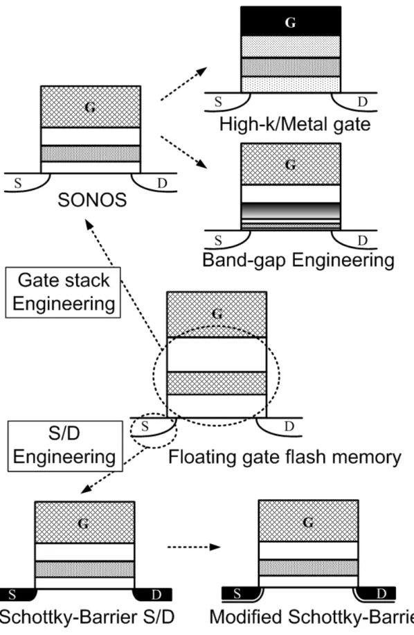
The gate engineering of flash memory has been widely mentioned in the last sections. These modifications on storage layers directly connect to the memory performance. However, gate stack is not the only part that can be modified to attain better performance. The modification of source/drain (S/D) structure also has strong impact on the memory performance. This modification is sorted as S/D engineering. The different methods to improve memory performance are shown in Figure 1-7. The following paragraphs show a brief introduction of Schottky-Barrier (SB) S/D and its potential of improving flash memory performance.
Nowadays, device scale-down has been proceeding on a hard road. SB MOSFET is again interesting. The motivations of applying SB S/D in advance MOSFET are its features of low parasitic S/D resistance, low temperature processing for S/D formation, elimination of parasitic bipolar action, and abrupt junctions for small gate length device [37]. In order to suppress ambipolar characteristic for SB-MOSFET, particular silicides have been chosen as the metal on S/D formation, including PtSi for PMOS, and ErSix or YbSix for NMOS [38-40]. However, the complimentary silicide add more process complexity on CMOS circuit and the on/off current of SB MOSFET is still not as good as conventional one. Modified Schottky-Barrier (MSB) S/D inherits the advantages of SB, and furthermore has competitive performance which depends on the effective SB height (SBH) lowering at source side and reduction of the tunneling leakage current at drain side [41]. The MSB also solve process complexity due to that it is composed of single mid-gap silicide like NiSi with a thin doping layer formed between silicide and channel.
The Schottky-Barrier S/D revealed memory application in the resent years. In 2000, the effect of Source-Hot-Electron (SHE) was discovered in SB MOSFET [42]. It means when electrons tunnel through Schottky-Barrier from source to channel, they
gain energy by the abrupt band bending. These hot electrons become easier to inject to gate or be stored in dielectric layer [43]. After that, a simulation work was reported and showed the prediction of that flash memory with SB S/D may has better program speed for Channel Hot Electron (CHE) programming [44]. The practical sample was first demonstrated by Chong in late 2008, it was formed by using Dopant-Segregation technique in tri-gate structure on SOI substrate [45-47]. The result stated obviously rising of program speed of Dopant-Segregation Schottky-Barrier (DSSB) S/D sample compared to conventional p-n junction S/D. And the improvement of program speed existed in both FN and CHE programming. The abrupt S/D band bending of DSSB seemed to lead to high program speed for FN programming. For CHE programming, source side injection was mentioned to explain the improvement of program speed. Since the abrupt band bending of MSB junction, the electrons are accelerated and get enough energy to emit to trapping layer at source side. In the conventional CHE programming, electrons have impact ionization and injection to trapping layer at drain side due to the pinch-off voltage drop there. Source side injection immunes the repelling between gate field and drain field during programming. So the rising of program speed occurs.
1-3 Motivation and thesis organization
As we mentioned in the above paragraphs, MSB S/D shows advantages on not only scale feasibility but also memory program speed. And ITS technique for forming MSB has the feature of low temperature process which especially matches the requirement on TFT device. We assumed that the TFT memory with MSB S/D can have good program speed and good competitiveness of making dense circuit. Besides,
the memory characteristics. For these reasons, this thesis investigates the ITS MSB S/D on memory devices with TFT and bulk substrate.
In this work, we selected SONOS as the gate stack since the fragility of the oxide on TFT channel could induce strong leakage and weak retention. Also SONOS stands out from device downscaling and it has the property for low voltage operation which connects to the low power consumption, the most important demand of portable electronics. Remarkably, MSB S/D can be made together with all advance SONOS structure mentioned in the previous paragraphs. It amplified the promise of installing MSB into the future flash memory. This thesis mainly focuses on the characteristics of TFT memory devices of different source/drain junctions such as conventional p-n junction, MSB junctions with variant process conditions of ITS technique, and pure SB junction. The detail contents in each chapter are listed below.
In chapter 1, the development of non-volatile memory is introduced. The feasibility of SB and MSB in memory device is also described. TFT flash memory is introduced. Indeed, the motivation of this thesis comes out from these understandings of flash memory, TFT, and MSB S/D.
In chapter 2, the experimental procedure which includes the design of device structure and the fully details of fabrication process flow is shown in this chapter. The analysis tools and methods are exhibited.
In chapter 3, the TFT memory samples are analyzed by two kinds of operation conditions, Fowler-Nordheim (FN) and Channel Hot Electron (CHE). The comparison of different program mechanism is discussed. The memory characteristics like retention and endurance are also measured and discussed.
Fig. 1-1: Schematic of Vertical Gate NAND array [6]. BL (Bit Line), WL (Word Line), SSL (Source Select Line), GSL (Ground Select Line), CSL (Column Select Line).
Fig. 1-3: Stress Induced Leakage Current (SILC) in floating gate (FG) non-volatile memory.
(a)
(b)
Fig. 1-5: Program/Erase band diagrams of (a) SONOS, and (b) MANOS. The benefits of MANOS are larger injection from channel and fewer back injection electron. The injection current to tunneling oxide increases due to that the replacement of high-k on blocking oxide results as higher field on channel surface. The back injection is suppressed because of the increasing the electron barrier at gate by the high work-function metal.
Chapter 2
Experimental Procedure
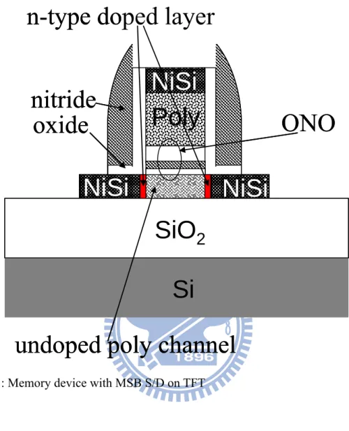
2-1 Device fabrication
In this section, we would like to describe the process methods of fabricating the modified Schottky-Barrier (MSB) S/D TFT memory samples. First of all, there are some design considerations of sample structure. We applied p-type poly-silicon gate in order to have high work function. The increased work function offers a higher electron energy barrier, so under negative bias the electron back injection could be suppressed and would not disturb the erasing efficiency. The blocking oxide was deposited up to 20 nm which is higher than the parameter on ITRS roadmap. Our concern is to eliminate the influence of back electron tunneling, which comes from the worried quality of the LPCVD TEOS oxide film, as much as possible. The spacer was fabricated as the two-layer structure. The under oxide layer is an etch-stop and stress-relief layer and also induces good contrast and distinguishable structure in microscopy image. The upper nitride layer is the blocking layer of gate and S/D in self-align silicide process. NiSi is the S/D contact metal in conventional S/D device and the Schottky-Barrier interface in the SB S/D or MSB S/D. NiSi is the most successful silicide so far in CMOS fabrication because of the low resistivity, robustness for making thin line, good thermal stability, and low forming temperature. For forming NiSi on TFT substrate, two-step formation is applied to prevent the lateral overgrowth of NiSi [19]. The first step is in low temperature to have slow and controllable lateral growth of Ni2Si. After removing the unreacted Ni, the second step
is a rapid thermal treatment to have phase transformation from Ni2Si to NiSi. The MSB junction was made by ITS technique which has been mentioned in previous chapter. The completed structure is shown in Figure 2-1.
In this thesis, the experimental focus is different S/D structures. The S/D structure can be clearly specified into SB, MSB, and conventional. The SB S/D is a pure silicide/silicon interface without any dopant-pile-up layer. The MSB S/D is a structure which has a dopant-pile-up layer adjacent to the NiSi/Si interface. If we modify the post implantation annealing time in ITS process, the different kinds of MSB S/D can be formed either SB-like or conventional-like since the concentration and thickness of the dopant-pile-up layer is varied. The conventional S/D has a typical p-n junction. The NiSi/Si interface is far from the junction and only behavior as ohmic contact metal. To entirely observe the memory characteristics of different S/D structure, five kinds of S/D structure are marked out to be the critical measure or analysis basis in this thesis, as shown in Table 2-1.
2-1-1 TFT sample
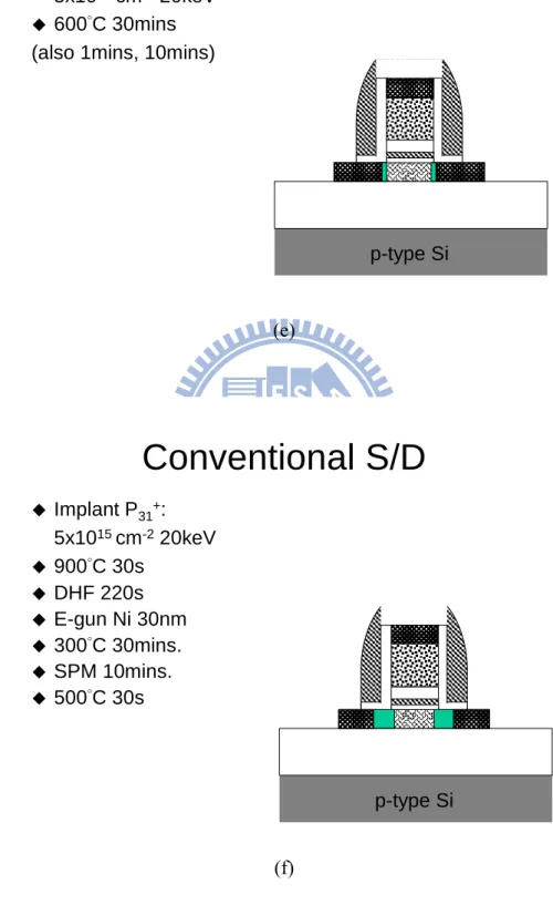
The process flow of SONOS TFT memory with MSB S/D started on 6-inch p-type wafers. Standard RCA clean was done as a pre-furnace clean. Before thermal oxide growth, wafers were immersed in diluted HF (HF:H2O=1:100) for 60s to remove native oxide. A 150-nm wet oxidation layer was grown as the back isolation insulator and then a 50-nm LPCVD amorphous Si layer was grown to be device channel. After that, wafers were annealed at 600°C in N2 ambient for 24 hours to have solid phase crystallization (SPC) in channel film. Following was thermal treatment at 900°C for 30 minutes in order to avoid the grains of poly-silicon channel film deformed under high temperature in the rest part of process. The active area definition
TCP9400 for isolation etching as shown in Figure 2-2(a). SC1 clean which is 10-minutes-immersion in the mixture of NH4OH:H2O2:H2O(1:4:20) at 75°C was applied to remove the polymers which were the by-products of silicon etching. RCA clean was done to guarantee the film quality of tunneling oxide. A 4nm/7nm/20nm-ONO (Oxide/Nitride/Oxide) stack was formed by LPCVD systems as the tunneling oxide/trapping layer/blocking oxide, and a 150-nm un-doped amorphous silicon layer was deposited as the gate electrode. P-type gate was made by implanting BF2+ at 40KeV to a dose of 5x1015 cm-2. Then, an 80-nm LPCVD TEOS layer was deposited as the gate etching hardmask and anti-doping protection during n+ S/D implantation. Gate patterning was done by i-line stepper, TCP9400, and TEL5000 which has recipes of SiO2 and Si3N4 anisotropic etching. A rapid thermal annealing at 900°C in O2 ambient for 20s was done to repair the dielectric damages caused by gate etching as shown in Figure 2-2(b). A 10-nm oxide and 50-nm nitride were deposited and etched to be the spacer as shown in Figure 2-2(c). The continuous process flows for making samples with different S/D structures, such as MSB S/D and conventional S/D, are stated in the following two paragraphs, respectively. For a clear view, there is a statement with the arranged symbols of samples and their split process conditions in Table 2-1.
To form the SB S/D, a 30-nm Ni layer was deposited by e-gun evaporation after immersed in dilute HF for 200s for removing the gate hardmask. Then, two-step silicidation was executed. It included annealing at 300°C in a vacuum chamber for 45 minutes immediately after Ni deposition, immersing in the solution of H2SO4:H2O2(3:1) for 10 minutes for removing the unreacted Ni, and rapid thermal annealing at 500°C for 30s as shown in Figure 2-2(d). Now, gate and S/D all had NiSi formation. To form the MSB S/D, the ion implantation was P31+ at 20keV to a dose of 5x1015 cm-2, the following was a 600°C annealing to let dopants segregate to
silicide/silicon interface and have activation. The post implantation annealing has a splitting as 1, 10, and 30 minutes to have a transition of MSB as shown in Figure 2-2(e).
To have the conventional S/D, S/D implantation was P31+ at 20KeV to a dose of 5x1015 cm-2 before NiSi formation. The rapid thermal annealing for dopant activation was at 900°C in N2 ambient for 30s. NiSi was formed to be contact metal. The process was the same with that NiSi formation in SB S/D except the 300°C annealing was shorten to 30 minutes, as shown in Figure 2-2(f).
2-2 Electrical characterization techniques
In this section, we would like to describe the methods to analyze the MSB S/D memory. The Current-Voltage (I-V) characteristics of our samples were measured by a precision semiconductor parameter analyzer of model Agilent 4156C. When we were operating memory device, the program or erase pulse signal was generated by the Agilent 41501A pulse generation expander. The threshold voltage (Vth) is defined as the applied gate voltage (Vg) at which the normalized drain current (Id) equals to 1x10⁻⁸A/μm as the voltage difference between drain and source (Vds) is 1V. The drain current is normalized by the gate length and width. The important memory characteristics and their measuring methods are described independently in the following sub-sections.
2-2-1 Read operation
There are three states in memory device. Initial state is the first time Id-Vg characteristic. After positive or negative voltage pulse, program and erase states are
different program or erase states. The gate voltage sweeping range is carefully selected, and it should be noted that inappropriate sweeping would cause misleading result of memory window. In our memory device, it is ease to reach a temporarily over-erasing state. The read operation on erase state must be controlled carefully or even measured repeatedly to make sure the state is stable. For particular case, forward read and reverse read are both measured. The only different between these two is the swapping of source and drain electrodes.
2-2-2 Program/Erase speed
The different pulse width versus Vth shift under certain voltage magnitude is the main characteristic to show memory speed performance. Each time before applying pulse, the memory should be manipulated to the same starting state. The starting state is a stable and locally saturated state. After a single pulse acts on device, the Vth is extracted. The difference of Vth before and after pulse shows the operation speed of memory. Both F-N and CHE programming were measured.
2-2-3 Retention
Retention is the characteristic which involves with the charge stored reliability. Normally, Vth shift versus the passing time after program or erase operation is used to indicate retention performance. Ten year is a milestone of this characteristic. It can be extrapolated from the Vth-versus-time curve. The accelerated test of increasing temperature is usually taken. For precise result, the Vth extraction must come from a suitable I-V sweeping and sample should place in a stable space and isolate from disturbance during measuring.
Endurance represents the robustness of memory device through many times of program and erase. In this thesis, a clock signal was applied as P/E cycles. The high-level voltage is for program and the low-level is for erase. The endurance was tested for the chosen P/E condition, which is with enough memory window and acceptable P/E speed.
Table 2-1: Sample ID and the process conditions of different S/D structures. Sample ID S/D Structure Process condition
PSB pure SB NiSi(300°C 45mins/500°C 30s)
M01 MSB NiSi(300°C 45mins/500°C 30s) + ITS(600°C 60s) M10 MSB NiSi(300°C 45mins/500°C 30s) + ITS(600°C 10mins) M30 MSB NiSi(300°C 45mins/500'C 30s) + ITS(600°C 30mins) CON p-n Activation(900°C 30s) + NiSi(300°C 30mins/500°C 30s) p.s. NiSi(1st step annealing/2nd step annealing); ITS(post implantation annealing)
Si
SiO
2
Poly
NiSi
NiSi
NiSi
nitride
oxide
ONO
n-type doped layer
undoped poly channel
Si
SiO
2
Poly
NiSi
NiSi
NiSi
Si
SiO
2
Poly
NiSi
NiSi
NiSi
nitride
oxide
ONO
n-type doped layer
undoped poly channel
Thin film formation
p-type Si Start on 6” wafer Wet oxide 150nm LPCVD a-Si 50nm SPC 600˚C 24hrs. 900˚C 30mins Pattern AA Dry etch poly-Si
PR strip
(a)
Gate stack formation
LPCVD TEOS 4nm LPCVD Nitride 7nm LPCVD TEOS 20nm LPCVD a-Si 150nm Implant BF2+: 5x1015 cm-2 50keV LPCVD TEOS 80nm Pattern Gate
Dry Etch TEOS
PR strip
Dry Etch a-Si
Dry Etch TEOS/Nitride
RTO 900˚C 20s
p-type Si (b)
Spacer formation
LPCVD TEOS 10nm
LPCVD Nitride 50nm
Dry Etch Nitride/Oxide
p-type Si (c)
NiSi formation
DHF 220s E-gun Ni 30nm 300˚C 45mins. SPM 10mins. 500˚C 30s p-type Si (d)ITS MSB formation
Implant P31+:
5x1015 cm-220keV
600˚C 30mins (also 1mins, 10mins)
p-type Si (e)
Conventional S/D
Implant P31+: 5x1015 cm-220keV 900˚C 30s DHF 220s E-gun Ni 30nm 300˚C 30mins. SPM 10mins. 500˚C 30s p-type Si (f)Fig. 2-2: Process flow of MSB TFT SONOS non-volatile memory. (a) isolation and channel film preparation, (b) gate stack formation, (c) spacer formation, (d) NiSi formation, (e) MSB formation, (f) Conventional S/D formation.
Chapter 3
Characteristics of the Thin Film Transistor
(TFT) Memory Device
3-1 Introduction
The memory characteristics of the thin film transistor (TFT) samples with different Source/Drain (S/D) structures are analyzed and discussed in this chapter. We focus on the individual performance of the memory samples on Table 2-1, which have various S/D structures. The comparison among the different S/D structures is also our focus. As mentioned in previous chapter, three kinds of memory samples are discussed: samples with pure Schottky-Barrier (PSB) S/D, with modified Schottky-Barrier (MSB) S/D, and with conventional (CON) p-n doped S/D. While SB junction and p-n junction have highly distinguishable properties, MSB junction is considered to be a transition type in between. The post implantation annealing time is the dominated process parameter for this transition. Characteristics of the MSB S/D memory devices with different annealing time are recorded to investigate the influence of the MSB S/D in flash memory device.
This chapter includes device structure inspection and the memory characteristics. TEM images are used to examine the device structure and the practical film thickness. As we know, flash memory has two kinds of layout. The NAND-type uses F-N tunneling programming, which is simple and less power consumption. On the other hand, in the NOR-type layout, devices can be programmed with a faster mechanism
a possible erase operation scheme because of the drain electrode separation. Electrical behaviors under FN program and CHE program will be discussed in different sections in order to have a clear explanation and discussion of the MSB S/D flash memory device.
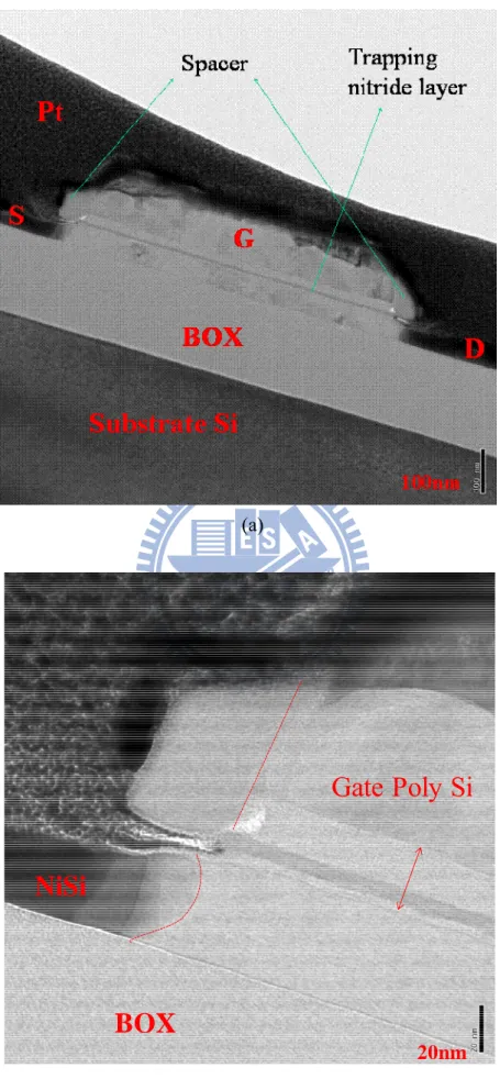
3-2 Device structure inspection
Figure 3-1 shows the Transmission Electron Microscopy (TEM) images of sample M30. Figure 3-1(a) is the cross-section view of the device. Spacer is well-functioned in the self-aligned silicide process so that NiSi on gate and S/D are formed properly. By Figure 3-1(b), the exact thicknesses of ONO films are measured : 3.6 nm of SiO2 as tunneling oxide, 6.8 nm of charge trapping nitride, and 18.8 nm of blocking oxide. The S/D structure is also shown in Figure 3-1(b). The lateral extending length of spacer is ~45 nm. An undercut on the bottom oxide layer of spacer was caused by the inevitable over-immersing in diluted HF for gate hardmask removing. Since the undercut does not extend to the channel, device characteristics would not be affected by that. The NiSi/Si interface is close to the channel edge which is defined by the edge of gate stack as the dot line shown in Figure 3-1(b). This promises a well MSB junction. The yield will loss if NiSi laterally-extend too much, due to the over-diffusion of Ni during anneal. Also, the contact of NiSi and tunneling oxide would degrade the robustness and should be avoided. A 3nm underlap between NiSi and poly-Si gate is measured.
3-3 Sample definition and basic I-V characteristic
The width and length of all measured devices are 1 μm and 0.35 μm. Sample conditions are listed in the previous chapter, Table 2-1. For the convenience of
description, samples are indicated as PSB, M01, M10, M30, and CON, which stand for their different S/D conditions.
Initial I-V characteristics are shown in Figure 3-2(a). Off-current, on-current, and sub-threshold swing (S.S.) are measured for all the samples. Due to the mid-gap work function of NiSi on Si, the PSB sample shows an obviously higher current at negative gate voltage. Also, comparing PSB and MSB samples, we find that with the ITS process, the off-current could be significantly decreased. The doped interfacial layer is able to eliminate the ambipolar characteristic effectively. Furthermore, comparing MSB samples, the off-current slightly reduces when longer post implantation annealing is taken. That reveals a transition between SB-like MSB and conventional-like MSB. Finally, the conventional sample shows the lowest off-state leakage.
The transition is also detected in the on-current change. We consider our sample as case of n-channel MOS. The improvement of on-current from PSB to M01 shows that the effective SB is lowered by the pile-up dopants at NiSi/Si interface. The on-current of M10 sample is dramatically increased. A 600 °C annealing for 10 minutes creates the extending doped layer at NiSi edge. This layer increases the gate controllability in the region between SB and channel edge. Longer annealing time is expected to make the MSB sample more conventional–like and increase the on-current. Overall, the PSB sample and CON sample show the lowest and highest on-current, respectively. The MSB samples are in between.
The sub-threshold swing (S.S.) of the curves in Figure 3-2(a) is 527, 547, 535, 746, and 1168 mV/decade for sample CON, M30, M10, M01, and PSB, respectively. The S.S. value (~550 mV/decade) for conventional-like sample is acceptable for TFT device. For samples more SB-like, such as M01 and PSB, higher S.S. values are
(SBH).
3-4 Memory characteristic of Fowler-Nordheim program
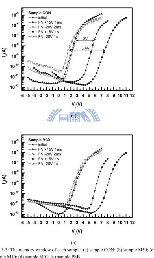
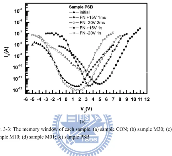
3-4-1 I-V characteristic and memory window
In Figure 3-3, the I-V curves of the program states and erase states of all the samples are demonstrated. Symmetric operation condition is set for all samples except sample PSB, which is hard to program. For those samples having well on-off ratio, including M10, M30, and CON, large memory windows can be achieved under 15 V gate program bias and -20 V erase bias in a 2-second P/E period. Also, they have acceptable windows (~3V) under millisecond-level P/E period with the same bias condition. On the other hand, the SB-like samples have poor S.S. or small windows which make them inapplicable. Also, for all samples, the Vth of erase-state is hard to become more negative than the Vth of initial state. The Vth of erase state could be smaller than of initial state after the entire trapped electrons are pulled out and the holes injecting from channel start to affect. In SONOS, hole-injection is comparatively weak since its energy barrier is relatively high and the Si3N4 layer is not a efficient hole trapping material. Negative shift could only be observed after a long erasing period [48-49].
3-4-2 Program/Erase speed
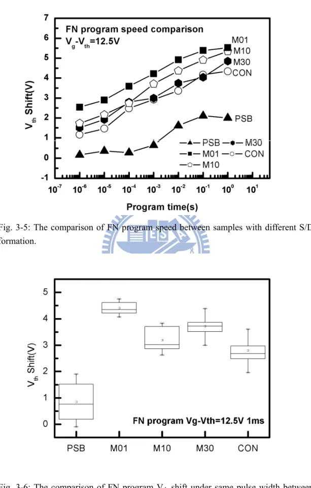
Under FN operation, samples CON, M30 and M10 all show well program speed as in Figure 3-4 (a), (b), and (c), respectively. After a 1-ms 15V gate voltage programming, the Vth shifts achieve up to 3V for M10, nearly 3V for M30 and CON. The program speed of sample CON is competitive to the devices with similar gate stack [2]. The sample M10, which has similar I-V characteristic with the sample CON,
reveals a slightly faster program speed. This guarantees the superiority of fabricating a MSB S/D in TFT memory by ITS technique. The MSB S/D with lower thermal budget and shorter process time takes a further worth value, as better program speed. Without addressing the problems of poorer S.S. and lower on-current, sample M01 shows a well program performance which has nearly 2 V window under Vg = 15V for 1 ms, as shown in Figure 3-4(d). As a whole view, the sample M01 is still out of application because of the insufficient I-V performance.
For a better comparison, we used the program bias with the same Vg-Vth, in order to have the same electric field in tunneling oxide. In Figure 3-5 and Figure 3-6, the rising up from PSB to M01 and the slightly up-going trend of CON, M30, and M10 are observed. The transition of pure SB to MSB and also the transition of MSB to conventional p-n junction will be discussed separately in the following two paragraphs.
In typical memory device, electrons enter channel region from S/D region to form inversion layer at high gate bias. These electrons are then tunneling into the Si3N4 layer by F-N tunneling. The S/D of sample PSB couldn’t be formed to overlap with gate since the reliability concern of NiSi growing. Therefore, from gate edge to source or drain NiSi, there is a region which is not directly controlled by gate. This region results in a potential barrier even at high programming voltage, as shown in Figure 3-7(a). The inversion layer cannot form as quickly as in typical memory device. Therefore, the program speed of the PSB device is very low. This region, which is hard to be controlled by gate, is modified when the MSB is formed since a doping layer is built over this region, as shown in Figure 3-7(b). So it can be inversed more effectively by the fringing field of high program voltage such as 15V. Moreover, the effective SB at S/D is lowered by the MSB formation, so electrons could have higher
sample M01 leads sample PSB better program speed, as shown in Figure 3-5 or 3-6. For comparison between MSB and conventional S/D, ten devices were measured for every process condition to eliminate the variance of TFT samples. Statistic result is shown in Figure 3-6. Sample M10 and M30 show better program speed potential compared to sample CON. For MSB, during programming, electrons from S/D would gain energy by the sharp SB-like band banding after thermionic passing SB. With higher energy, electrons become easier to inject into the nitride layer, as the band diagram in Figure 3-8(a). Larger threshold voltage shift under the same program operation occurs in MSB S/D TFT memory. However, the program speed improvement in our work is not as large as the reference, which has samples fabricated on single crystal silicon and with tri-gate structure and thinner blocking oxide [46]. The missing of great program speed improvement is suspected as the consequence of making MSB S/D memory on the TFT substrate. Due to the poly silicon channel, the acceleration of MSB sharp band bending becomes much weaker. Most of the electrons couldn’t gain enough energy from SB band bending since the acceleration path is full of defects and grain boundaries. The electrons would be scattered severely and only the less part of electron would have the expected high kinetic energy, as shown in Figure 3-8(b). If the channel is single crystal, the electron could all be accelerated efficiently and all become much easier to inject into nitride layer. However, it is possible that the tri-gate corner effect or thinner ONO layers in the reference [46] amplify the improving factor of MSB S/D in program speed performance.
In our case of FN erase, negative bias is connected on gate electrode. It offers the reverse band bending on the gate stack and forces the electrons stored in nitride moving out by FN tunneling. Figure 3-9 shows the erase Vth shifts under the same pulse as Vg = -18V for 1 ms of all samples. Between each sample, no apparent
difference is detected. This is because of that S/D formation doesn’t affect the mechanism of FN erasing since repelling electrons out of trapping layer only depends on the electric field in the tunneling oxide. Thus, all the samples with the exactly same gate stack have the identical erase speed. The FN erase speed diagrams of sample CON, M30, M10, M01 are shown in Figure 3-10, respectively. Under the bias of Vg = -20 V, the acceptable erase shift is realized within a millisecond pulse for these samples.
3-4-3 Retention and endurance
Figure 3-11 indicate the large window memory retentions of sample CON, M30, M10, and M01. All samples have the around 50% charge loss on ten-year retention approximation. Retention characteristic with small window in shorter P/E cycle is measured to eliminate the repulsive effect of accumulated charges. The result is nearly the same 50% charge loss. Also, there is no apparent difference between memory samples with different S/D structures. We believe that retention characteristic is also mostly determined by the structure and film quality of ONO stack. In this case, the non-thermally grown thin SiO2, as tunneling oxide, shows the weakness of blocking leakage for retention characteristic. Moreover, the rough interface between poly silicon channel and tunneling oxide causes the retention loss.
In this thesis, poor endurance characteristic is detected in all of the samples, as shown in Figure 3-13. The hard-to-erase effect is observed in all samples, as that the memory window obviously shrinks at the erase side after 104 P/E cycles. In each P/E cycle, some electrons which stored in the deep level of nitride become hard to pull off. Eventually, those electrons accumulate to an enough amount to make memory window positive shift after numerous P/E cycles.During P/E cycles, blocking oxide is
becomes severer after numerous P/E cycles and it would decrease the erase ability of negative bias. This makes the positive shift of erase state is larger than of program state.
In addition, the I-V curves of the devices after 104 P/E cycles are examined to find more information of the losing memory window. It is clear that sample M01 and M10 have sub-threshold swing degradation but sample CON doesn’t, as shown in Figure 3-14. The degradation induces positive Vth shift of erase state and negative Vth shift of program state. Since the MSB samples have injection electrons with higher energy, more interface states are generated between channel and tunneling oxide, which result in sub-threshold swing degradation, after numerous P/E cycles. The non-uniform stored charge is the potential reason which leads to swing degradation since TFT memory device is with the rough interface of poly silicon channel and tunneling oxide. Moreover, the SB-like MSB sample tends to have injection near S/D or even out side the gate area. After numerous P/E cycles, inevitable accumulated electrons in spacer region starts to interfere the memory characteristic. Therefore, even the total electrons in the nitride trapping layer are cleaned, the erase state is still influence by the field from the spacer trapping which leads to its positive shift. Also, this spacer trapping would lower the program efficiency since the generated field limits the electron injection from S/D. The swing degradation and charges trapped outside gate cause the SB-like MSB samples have more memory window loss than the conventional samples.
3-5 Memory characteristic of channel hot electron program
3-5-1 Basic I-V characteristic and memory window
After channel hot electron (CHE) program, the I-V characteristic and memory window reveals differences in forward read and reverse read since charges are not
uniformly stored in nitride layer. The effect of the trapped electrons distribution is shown in Figure 3-15. If electrons are mostly trapped near drain side, forward read would have larger off-state leakage current and reverse read would gain slightly more Vth shift. Those electrons stored near drain side offer the field such like locally connecting to a negative bias. In off-region, gate induced drain leakage (GIDL) effect is enhanced by this field. Indeed, TFT poly silicon substrate is affected by a severer trap-assisted GIDL [49]. During reverse read, the electrons stored at drain side raises the electrons injection barrier from drain to channel by pulling up the energy band. This results in more positive Vth shift. If electrons are mainly stored at source side, the features are opposite, larger off-state leakage in reverse read and larger Vth shift in forward read.
In conventional flash memory, CHE injection happens at drain side due to the large voltage drop of pinch off region. As usual, sample CON shows drain side injection, which has up-swung off-current under negative gate bias in forward read and larger memory window for reverse read, as shown in Figure 3-16(a). In sample PSB, I-V characteristic reveals source side injection features, which is larger Vth shift in forward read and higher off-current in reverse read, as shown in Figure 3-16(b). The sharp SB-like band bending accelerates electron after it goes over source side SB, so electron gains enough energy to inject at source side.
For MSB S/D, sample M30, M10, and M01 all have higher off-current in forward read and larger Vth shift in reverse read, as shown in Figure 3-16(c)(d)(e). Those features prove that the TFT memory device with MSB S/D structure, formed by ITS technique, tends to have drain side injection. This is an opposite phenomenon compared to the reference with DSSB S/D on SOI substrate, which shows source side injection [47].
3-5-2 Program/Erase speed
In CHE programming, good program speed only exists in sample CON, as shown in Figure 3-17(a). After a 1-ms CHE program at Vg = 10V and Vd = 6V, sample CON has Vth shift as ~2.5 V. In spite of the less efficient program speed compared to FN programming, CHE programming still has application if the design requirement is low voltage operation. Since poly silicon channel has low electron mobility, the amount of hot carriers in TFT memory device is much fewer than device on single crystal silicon. Therefore, in TFT memory device, CHE program efficiency is no longer the same or higher level compared to FN program. The memory device with MSB S/D structure is also influenced by the poly silicon in much worse case. Sample M10, which has similar I-V characteristic with sample CON, doesn’t share the similar memory characteristic. After a CHE program pulse with Vg = 10V and Vd = 6V for 1 ms, sample M10 only has a small Vth shift as 1 V, as shown in Figure 3-17(b). Extending the post implantation annealing in ITS process makes device having more conventional-like characteristic. Due to the more conventional-like S/D, sample M30 behaves better CHE program speed, as shown in Figure 3-17(c). The lower thermal budget and less process time consumption MSB S/D is still possible to apply on TFT substrate and for CHE operation if the conventional-like MSB S/D is formed. The insufficient program speed can be made up by extending the post implantation annealing or by setting higher operation voltage as a trade-off. In Figure 3-17(d), the condition which sample M01 has enough Vth shift is only in long program time or high program voltage. However, both of the modifications are unwanted, so the SB-like MSB S/D is out of application.
For comparison between SB, MSB S/D, and conventional S/D TFT memory device in CHE programming, ten devices are measured for each process condition to eliminate the variance of TFT samples. The statistic result is shown in Figure 3-18.
The constant Vg-Vth is used in order to have same vertical field in tunneling oxide. The transition from MSB to conventional p-n junction shows the increasing program speed which is opposite to FN program. And there is no CHE program speed change through the transition from sample PSB to sample M01. That sample M10 and sample M30 perform worse than sample CON in CHE program speed is caused by three factors, which includes the lower electron injection rate from source to channel, the voltage drop share at source side SB, and the grain boundaries in poly silicon channel. As the explanation in the reference which shows improving CHE program speed in DSSB S/D memory [47], source side voltage drop caused by SB junction would let the electrons have source side injection. This source side injection in MSB S/D is stronger than drain side injection in conventional S/D since there is no bias at source side to cancel gate voltage field. If the channel is single crystal, electrons passing SB could gain enough energy to become hot carrier at source side. This would cause a great improvement in CHE program speed. However, our samples are fabricated on poly-silicon substrate and that makes the path of acceleration by SB band bending full of grain boundaries. If the electron meets the grain boundaries and is scattered, it does not become a hot carrier, which is easier to inject. The acceleration to build hot electrons at source side is degraded, as shown in Figure 3-19. Even though the acceleration at source side is vanished, electrons still get chance to inject to trapping layer at drain side voltage drop just like the conventional S/D but the drain side injection in MSB S/D device is not competitive to the drain side injection in the conventional S/D. In MSB S/D memory device, source side SB consumes a part of voltage drop, so it doesn’t have electrical field as high as conventional S/D memory during program operation. Also, the low electron injection rate from source to channel makes the MSB S/D sample behaves worse since the supply of electron is basically
Under the same program cycle, the Vth shift is nearly equal for sample PSB and sample M01. As the discussion of I-V characteristic above, sample PSB shows source side injection. This is simply the result of the lack of electron supply from source to channel. That the total amount of electrons decreases to a really low level makes the source side injection become the dominated part. In MSB S/D device, source side injection part is the less part since the supply is plenty and the electrons which can not be injected at source side would finally go to drain. In this way, source side injection of sample PSB isn’t a bursting injection caused by the acceleration of SB band bending, so there is no practical advantage for it.
The erase operation after CHE program is set to be FN tunneling. Vth shifts under the same pulse as Vg = -18V for 1 ms of all samples are shown together in Figure 3-20. Just like the FN erase after FN program, there is no difference for the erase speed between CON sample and MSB samples. Since the injected electrons of CHE program are trapped locally and have higher energy, we find that electron programmed by CHE is much difficult to pull off the electrons in trapping layer and more unstable. As shown in Figure 3-21, band to band hot hole (BBHH) injection only works on sample CON since the MSB sample doesn’t have the overlapped and highly doped n-type layer to generate hot hole. For MSB sample, the amount of injecting holes is in a poor level. Also, the injection position of holes is not totally match the electron stored position. Therefore, instead of Vth shift back, this few holes cause the lowering of off-current in sample M10 after BBHH erase, as shown in Figure 3-22 (a). It is interesting that sample M01 has the slightly positive shift after BBHH erase. The I-V characteristic is shown in Figure 3-22 (b). The conservation of off-current in reverse read curves shows that source side doesn’t involve. For forward read, electron stored near drain interface is neutralized by hole-injection and off-current become lower. The positive Vth shift is assumed as the effect of slight
electron back injection in channel region. The diagrams of CHE erase speed versus erase time are shown in Figure 3-23. For conventional sample, both FN and BBHH erase can be applied after CHE program. BBHH is even better. For MSB sample, FN erase as -20V gate voltage is enough for erasing charge by CHE program. Since the MSB are not totally drain side injection and the efficiency of generating hot hole is poor in MSB S/D, the erase ability of FN mechanism is better than BBHH.
3-5-3 Retention and endurance
The retention characteristics of sample CON, M30, M10, and M01 operated under CHE program and FN erase are shown in Figure 3-24. Longer P/E time, even up to 100 msec or 1 second, is set for MSB samples due to their poor CHE program efficiency. Only sample CON can span memory window up to 2V under millisecond level P/E period. Just like FN retention, the poor charge keeping ability of the thin LPCVD TEOS oxide on poly silicon causes the window loss in CHE retention. Sample CON has 65% window remained in the ten years approximation. The others are at the same level. Since the retention characteristic is determined by the tunneling oxide quality. Keeping a thin oxide film with leakage immunity on a rough poly silicon surface is important to a successful TFT flash memory. Adjusting the thickness of oxide or applying high dielectric constant dielectrics are possible solution.
The endurance characteristics of CHE operation is shown in Figure 3-25. Sample CON and sample M30 have a stronger positive window shift after 104 P/E cycles. The weaker erasing efficiency and the local high energy injection make the hard-to-erase easier to happen. On the other hand, samples with MSB S/D, especially sample M10 and sample M01, have less hard-to-erase phenomenon. This is because of that the charge injection position is not concentrated in drain-side region during CHE
M30 after 104 P/E cycles are extracted, as shown in Figure 3-26. The conventional S/D memory device has a larger voltage drop at drain side than conventional-like MSB S/D memory. It means that the injected electrons have higher energy in sample CON than in sample M30, so more interface states is generated in sample CON. It results in that much severe swing degradation happens in sample CON after numerous P/E cycles.
3-6 Summary
Under FN program, MSB S/D flash memory has a slightly program speed improving, compared to conventional S/D and pure S/D, due to the sharp SB band bending at S/D. The grain boundaries in TFT channel reduces the FN program speed improvement from MSB S/D since electrons wouldn’t be fully accelerated by the sharp SB band bending as expect. Electron would be scattered by the grain boundaries before it gains enough kinetic energy. The enhancement of program speed by MSB S/D is degraded when memory device is fabricated on TFT substrate. Despite all, for program efficiency, MSB S/D TFT memory still leads slightly in FN programming but it falls much behind in CHE programming. Memory device with MSB S/D has the lower speed compared to conventional S/D in CHE program. The degradation of acceleration near the source SB makes source side injection vanished. Even though the effective SB height of MSB is lowered by the thin n-type doped layer and also band bending is sharper, the electrons are still not able to become hot carriers at source side because of the scattering caused by the grain boundaries. This makes MSB S/D TFT memory device showing drain side injection. However, CHE program speed of MSB S/D is not competitive to conventional S/D which has sharper drain side band bending. The non-overlap S/D formation causes sample PSB to have worst
performance in FN programming. In CHE programming, the source side injection of sample PSB comes from the lack of electron supply caused by the large electron barrier at source junction. Actually, this kind of source side injection doesn’t help in program efficiency.
During FN erasing, the feature is almost the same for MSB and conventional for FN or CHE program. The effect of channel engineering is negligible in the mechanism of pulling off trapped electrons from nitride layer. BBHH erase has strong effect in sample CON, due to the overlapped highly doped n-type region. On the other hand, in MSB sample, hot holes are hard to generate and results in zero erase Vth shift for BBHH.
Our samples suffer from worse charge retention since the quality of tunneling oxide is degraded by the rough poly grains. In FN program endurance characteristics, all samples shows hard-to-erase phenomenon, which is full window positive shift. The Vth positive shift in erase state could come from the degradation of block oxide quality after P/E cycles stress. Further, MSB samples have less positive Vth shift in program state since the charges trapped outside gate lower the program efficiency. In CHE program endurance characteristics, sample CON shows much strong hard-to-erase phenomenon since electron injection of sample CON during CHE program is concentrated in drain side region. For swing degradation, the memory devices with higher electron energy during programming have earlier happening degradation of sub-threshold swing, as the MSB S/D in FN programming and the conventional S/D in CHE programming.
(a) 20nm
Gate Poly Si
BOX
NiSi
(b)(a)
(b)
Fig. 3-3: The memory window of each sample. (a) sample CON; (b) sample M30; (c) sample M10; (d) sample M01; (e) sample PSB
(c)
(d)
(e)
Fig. 3-3: The memory window of each sample. (a) sample CON; (b) sample M30; (c) sample M10; (d) sample M01; (e) sample PSB
(a)
(b)
(c)
(d)
Fig. 3-4: The FN program speed of each sample. (a) sample CON; (b) sample M30; (c) sample M10; (d) sample M01;
![Fig. 1-2: Schematic of Vertical Cell NAND array [7].](https://thumb-ap.123doks.com/thumbv2/9libinfo/8204009.169641/23.892.218.697.540.942/fig-schematic-vertical-cell-nand-array.webp)
![Fig. 1-6: Band-gap Engineering [13-14]](https://thumb-ap.123doks.com/thumbv2/9libinfo/8204009.169641/26.892.152.730.101.857/fig-band-gap-engineering.webp)