基於 Disksim 之 NAND 快閃記憶體磁碟模擬器
39
0
0
全文
(2) 基於 Disksim 之 NAND 快閃記憶體磁碟模擬器 A NAND Flash Disk Simulator Based on Disksim. 研 究 生:郭特民. Student:Te-Ming Kuo. 指導教授:張瑞川. Advisor:Ruei-Chuan Chang. 國 立 交 通 大 學. 資訊學院 資訊學程 碩 士 論 文. A Thesis Submitted to College of Computer Science National Chiao Tung University in partial Fulfillment of the Requirements for the Degree of Master of Science in Computer Science June 2008 Hsinchu, Taiwan, Republic of China. 中華民國九十七年六月.
(3) 中文摘要. 基於. Disksim. 之. NAND. 快閃記憶體磁碟模擬器. 學生:郭特民. 國 立 交 通 大 學. 指導教授:. 資 訊 學 院. 摘. 張瑞川. 資 訊 學 程 碩 士 班. 要. Disksim 具有效率、精確、高度彈性的特性,能模擬磁碟、控制器、匯流排、 驅動程式、排程程式、磁碟快取記憶體、磁碟陣列等儲存系統的效能,因此廣泛地 應用於儲存系統研究中。然而,在要求質輕、省電的嵌入式系統中,大部份是採用 快閃記憶體為儲存媒介,其中尤以 NAND 快閃記憶體較適合作為資料儲存之用。 然而,Disksim 只適用於磁碟系統,因此本研究的目的就是在既有的 Disksim 4.0 功 能外,加入 NAND 快閃記憶體儲存裝置及控制器,延伸其功能使其適用於快閃記 憶體儲存系統。 我們首先研究 Disksim 的執行環境,分析其輸入、輸出,以了解其功能與特 性。然後我們分析常見之快閃記憶體儲存系統的硬體架構,歸納這些系統的拓撲架 構定義,因此定義本論文所需實作的 Disksim 快閃記憶體裝置、控制器軟體模組及 其效能統計參數。我們參考多份廠商公布之快閃記憶體規格,定義快閃記憶體裝置 的存取時間參數,並實作控制器的 FTL 界面作為範例,可為後續修改 FTL 之參 考。 我們使用內建快閃記憶體控制器的 RTD2950 作為實驗帄台,比較存取 Hynix HY27UF082G2B 的命令時間與 Disksim 修改後的模擬結果,誤差僅在 5.84%以 內,因此證實本研究之實用性與正確性。. i.
(4) 英文摘要 A NAND Flash Disk Simulator Based on Disksim Student: Te-Ming Kuo. Advisors: Dr. Ruei-Chuan Chang. Degree Program of Computer Science National Chiao Tung University. ABSTRACT Disksim is an efficient, accurate and flexible storage system simulator that can simulates the performance of disks, controllers, buses, drivers, schedulers, disk caches and disk arrays.. It is widely adopted in the storage system research.. Due to the. light-weight and low-power requirements, most embedded systems use flash memory, especially NAND flash, as storage. However, Disksim does not support flash storage. In this paper, we extend the functionality of Disksim 4.0 to flash storage systems via adding flash device and controller modules. To achieve the goal, we first study the execution environment of Disksim and evaluate its input and output to understand its functionality. We then analyze the hardware architecture of flash storage systems and their topologies. Finally, we extend Disksim by implementing flash device and controller modules.. The performance. parameters of the flash device and controller modules are obtained from datasheets of several flash chips. Moreover, the controller module includes an implementation of the FTL callback as a reference for further flash storage research. We use a real hardware platform (i.e., RTD2950 with a built-in NAND controller and a HY27UF082G2B NAND flash chip) to measure the accuracy of the results reported by the extended Disksim. The experimental results show that the error of the extended Disksim is within 5.84%, demonstrating the usability and accuracy of our work.. ii.
(5) 誌謝 感謝張瑞川教授及張大緯教授在本人研究方向、方法的諸多指導,以及許多寶 貴時間,讓學生在工作之餘仍得以領略研究工作,進而運用到工作、生活之中。. iii.
(6) 目錄 中文摘要 ............................................................................................................. i 英文摘要 ............................................................................................................ ii 誌謝 ...................................................................................................................iii 目錄 ................................................................................................................... iv 表目錄 ................................................................................................................ v 圖目錄 ............................................................................................................... vi 一、緒論 ............................................................................................................ 1 二、研究方法 ..................................................................................................... 5 2.1 Disksim 4.0 架構 ...................................................................... 5 2.1.1 輸入與輸出 ............................................................................... 5 2.1.2 軟體架構 ................................................................................. 11 2.2 模擬器的應用 .......................................................................... 12 2.2.1 簡易型嵌入式系統 .................................................................. 12 2.2.2 攜帶型儲存系統 ...................................................................... 12 2.3 快閃記憶體裝置模擬檔 (disksim_nand.c) 實作 ................... 13 2.3.1 存取時間參數 .......................................................................... 14 2.3.2 效能統計輸出 .......................................................................... 20 2.4 快閃記憶體控制器模擬檔的實作 .......................................... 20 2.4.1 ioreq_event flags 的定義 ........................................................ 20 2.4.2 控制器的參數 .......................................................................... 22 2.4.3 快閃記憶體轉換層(FTL) ........................................................ 23 2.4.4 效能統計輸出 .......................................................................... 23 三、實驗與結果 ............................................................................................... 24 3.1 實驗帄台 ................................................................................. 24 3.2 Disksim 環境設定 .................................................................. 25 3.3 實驗結果 ................................................................................. 26 四、結論 .......................................................................................................... 29 參考文獻 .......................................................................................................... 30. iv.
(7) 表目錄 表 表 表 表 表 表 表 表 表. 1:NAND/NOR 快閃記憶體比較表[] ........................................................ 2 2:各家廠商 NAND 快閃記憶體命令集比較表 ....................................... 13 3:快閃記憶體裝置支援命令集及其使用時機 ........................................ 14 4:快閃記憶體時間參數表[8] ................................................................... 14 5:struct ioreq_event 相關欄位說明 ......................................................... 20 6:RTD2950 性能諸元 ............................................................................. 25 7:單一命令之模擬與實驗時間比較表 .................................................... 27 8:Busy time 比較表 .................................................................................. 27 9:更新參數後之模擬與實驗時間比較表 ................................................ 28. v.
(8) 圖目錄 圖 圖 圖 圖 圖 圖 圖 圖 圖 圖 圖 圖 圖 圖 圖 圖 圖 圖 圖 圖 圖 圖 圖 圖 圖 圖 圖 圖 圖 圖. 1:NAND 快閃記憶體組織示意圖[20] ...................................................... 2 2:NAND 快閃記憶體存取界面示意圖[20] .............................................. 3 3:NAND 快閃記憶體存取界面訊號說明[20] .......................................... 3 4:Disksim 4.0 輸入/輸出示意圖 ............................................................ 6 5:自定 trace 格式之程式碼示例 .............................................................. 6 6:初始化自定格式表頭的程式碼示例 ...................................................... 7 7:參數檔示例圖 ......................................................................................... 9 8:io_printstats() 程式示意圖 ................................................................... 11 9:Disksim 軟體架構圖 ............................................................................ 12 10:嵌入式系統之快閃記憶體應用架構圖 .............................................. 12 11:拇指碟或記憶卡的應用架構圖 .......................................................... 13 12:Command Latch Cycle [20] ................................................................. 16 13:Address Latch Cycle [20] .................................................................... 16 14:Sequential Out Cycle after Read[20].................................................... 17 15:Read Page Timing[20] ......................................................................... 17 16:Page Program Timing[20] .................................................................... 18 17:Block Erase Timing[20] ....................................................................... 18 18:Status Read Timing[20] ....................................................................... 19 19:Cache Program Operation .................................................................... 19 20:struct ioreq_event ................................................................................ 21 21:ioreq_event flags 欄位的定義 ............................................................ 22 22:struct controller .................................................................................... 22 23:controller param 定義 ......................................................................... 22 24:控制器能力與事件旗標關係(disksim_ctlrnand.c)示例圖 .................. 23 25:RTD2950 實驗帄台............................................................................ 24 26:HY27UF082G2B 照片 ....................................................................... 24 27:實驗環境拓撲設定 ............................................................................. 25 28:實驗環境拓撲架構圖 ......................................................................... 26 29:NAND0 specification using typical value (RTD2950.parv) ................. 26 30:NAND0 specification using measured value (RTD2950_fix.parv) ....... 28. vi.
(9) 一、緒論 在儲存系統的研究領域,為了改善輸入/輸出(I/O)效能,很多研究 探討儲存裝置的特性[1,2,3,4,5]。其中 Disksim[6] 在這些研究上扮演非常重要的 角色,它具有效率、精確、高度彈性的特性,能模擬磁碟、控制器、匯流排、 驅動程式、排程程式、磁碟快取記憶體、磁碟陣列,使其廣泛地被採用於研究 之中,而說是非常重要的工具。然而,Disksim 是以磁碟為儲存裝置的模擬器。 而在要求質輕、省電的嵌入式系統中,大部份是採用是以快閃記憶體[7]為儲存 媒介。 快閃記憶體主要分為二種:NAND 和 NOR。NAND 與 NOR 的比較表如 表 1,這些不同的特性造成二者應用領域不盡相同。NOR 可支援程式碼執 行,讀取速度較快,寫入速度較慢,但無法達成較高的儲存密度。而 NAND 可 提供較大的容量,但無法支援程式碼隨機讀取、執行,而 NOR 可支援程式碼 執行,讀取速度較快,寫入速度較慢,但無法達成較高的儲存密度,這些不同 的特性造成二者應用領域不盡相同,因此 NAND 被廣泛地運用於大容量的儲存 系統。圖 1 說明 NAND 快閃記憶體的組織[8]。一個 NAND 快閃記憶體是由 若干 block 組成,而每個block 通常是由32 或 64 個 page 構成,每個 page 是 512 字元 (small block) 或 2048 字元 (large block)。 圖 2[8]是 NAND 快閃記憶體的存取界面示意圖,圖 3[8]是界面訊號說 明。由於 NAND 有 8-bit 與 16-bit 二種界面,IO15 ~ IO8 只在 16-bit 的晶片才 有。由此可知快閃記憶體的存取特性[9]與傳統磁碟大為不同,例如:快閃記憶 體沒有旋轉機構、存取時間的參數不同、快閃記憶體得經過抹除程序後才能將 資料由 0 變 1,之後才能再被寫入一次,而且抹除的次數是有限的,通常約一 萬次至一百萬次,之後有可能造成類似硬碟壞軌的情況,此壞掉的抹除單位稱 為 bad block。前述的存取特性造成管理快閃記憶體的困難,通常為了讓快閃記 憶體可以在原有的檔案系統(NTFS[10], FAT16/32, EXT3)下運作,最常採用 的 一 種 方 法 是 快 閃 記 憶 體 轉 換 層 ( Flash Translation Layer, FTL ) [11,12,13,14,15,16]。FTL 藉由將邏輯區塊位置(logical block address)對應到快閃記 憶體的真實位置,因此可將快閃記憶體視為連續的儲存空間,便可在原系統環 境下當成儲存裝置使用。為了做好 bad block 管理,就要考量 wear-leveling[17], 均勻使用各區塊,管理已被寫入的區塊,適時清除、回收 (garbage collection)。 1.
(10) 表 1:NAND/NOR 快閃記憶體比較表[18] 項. 目. NAND. NOR. Capacity. 16MB to 4GB. 1MB to 32MB. Perforance. Fast erase, fast write, fast read. Slow erase, slow write, fast read. Program unit. Page. Byte/Word. Erase unit. Block (16~128KB). Sector/block. Ideal usage. Data. Code. Erase cycle. 100,000 ~ 1,000,000. 10,000 ~ 100,000. Reliability. Low, requires 1~4 bits. Standard. ECC/EDC and bad block management Access method. Sequential. Random. Cost per MB. Low. High. 圖 1:NAND 快閃記憶體組織示意圖[20]. 2.
(11) 圖 2:NAND 快閃記憶體存取界面示意圖[20]. 圖 3:NAND 快閃記憶體存取界面訊號說明[20]. 近來 SSD (Solid-State Drive) 快速崛起,在筆記型電腦及個人電腦的應用也 愈來愈廣泛,其中使用的就是快閃記憶體。我們預期,以半導體技術生產的快 閃記憶體儲存媒介未來會在儲存系統佔有一定的比例。因為快閃記憶體的特性 與限制與傳統磁碟不同,近來以快閃記憶體為基礎的儲存系統之相關研究開始 興盛。然而,如前所述,即使 Disksim 已在磁碟系統的研究領域有卓越成就, 可是它的缺點就是只適用於磁碟,我們仍沒有旗鼓相當的模擬器輔助快閃記憶 體儲存系統。本研究的目的就是在既有的 Disksim 4.0 功能外,加入 NAND 快 閃記憶體儲存裝置及控制器,使其適用於快閃記憶體儲存系統,進而成為快閃 3.
(12) 記憶體儲存系統研究(例如:FTL,Flash 檔案系統研究)的實驗與效能評估帄 台。 在此研究中,我們首先研究 Disksim 的執行環境,分析其輸入、輸出,以 了解其功能與特性。然後我們分析常見之快閃記憶體儲存系統的硬體架構,歸 納這些系統的拓撲架構定義,進而定義本論文所需實作的 Disksim 快閃記憶體 裝置(disksim_nand.c)、控制器(disksim_ctlrnand.c)軟體模組及其效能統計參數。 此二模組均可透過 Disksim 原有之參數檔輸入其參數與功能之設定,持續保有 其彈性之優點。我們參考多份廠商公布之快閃記憶體規格,定義快閃記憶體裝 置的存取時間參數,並實作控制器的 FTL 界面作為範例,可為後續研究修改 FTL 之參考。 我們使用內建快閃記憶體控制器的 RTD2950 作為實驗帄台,比較存取 Hynix HY27UF082G2B 的命令時間與 Disksim 修改後的模擬結果,誤差僅在 5.84%以內,證實本研究之實用性與正確性。 本論文其餘的章節組織如下:第二章描述 Disksim 的執行方法、軟體架構 及相關的快閃記憶體儲存系統應用、本論文定義的重要之快閃記憶體存取參 數及 Disksim 之實作修改。第三章描述實驗的環境與達到的成果。第四章綜整 本論文研究之成果與貢獻。. 4.
(13) 二、研究方法 為了沿用 Disksim 的架構及其主要軟體功能,我們思考的是如何加入快閃 記憶體這個模組,因此參考 Disksim 的磁碟裝置為原型,另外新 增 disksim_nand.c 為快閃記憶體裝置。此外,快閃記憶體特有的區塊抹除(Block erase)功能,必頇主動地由控制器判斷執行抹除、回搬(copy back program) 時機與區塊位址,因此我們另新增記憶體控制器 disksim_ctlrnand.c 作此功能之 用,以下即針對 Disksim 4.0 架構、快閃記憶體裝置與控制器作一說明: 2.1. Disksim 4.0 架構. 2.1.1. 輸入與輸出 Disksim 4.0 執行時需定義系統的拓撲架構,定義於圖 4 的 parameter file. 中,其格式可參考 Disksim 手冊[6] ,目的是透過參數檔設定不同模組的參數值 以發揮彈性,達到支援不同種類儲存系統的功能。 模擬的事件則由 trace file 輸入,其支援多種格式,常見的 ascii 格式定義 為:<time> <dev No.> <block No.> <block count> <flag>: (1) time 是事件到達的的時間, 以毫秒為單位,在檔案內頇以時間先後順 序排序。 (2) dev No. 是一個整數,用來代表事件要存取的裝置代號。 (3) block No. 是代表 I/O 事件所存取的第一個區塊位址。 (4) block count 是代表 I/O 事件存取的區塊個數。 (5) flag 是用來提供此事件的額外資訊,例如:位元 0 若為 1 表示是 read, 0 表示是 write。其他位元的定義可參考 disksim-4.0/src/disksim_global.h Info file 則是模擬輸出,包含拓撲架構中各模組的性能數值。 Parameter file. Disksim 4.0. Trace file 5. info. file.
(14) 圖 4:Disksim 4.0 輸入/輸出示意圖 1. Trace 檔案 目前 disksim 支援以下幾種格式: (1) ascii (2) hpl, hpl2 (3) dec (4) atabus (5) ipeak (6) postgres (7) emcsymm (8) emcbackend (9) batch 而且可以很容易地修改,以支援其他自定的格式,其步驟如下: (1) 在 disksim_global.h 中另定一格式的常數 (2) 將這格式取一字串名稱,並在 disksim_iotrace.c 中的iotrace_set_format() 副程式中加入字串名稱比較的程式碼 if (strcmp(formatname, "0") == 0) { disksim->traceformat = DEFAULT; } else if (strcmp(formatname, "ascii") == 0) { /* default ascii trace format */ disksim->traceformat = ASCII; } else if (strcmp(formatname, "xxxx") == 0) { /* User-defined format */ disksim->traceformat = XXXX; 圖 5:自定 trace 格式之程式碼示例 (3). 在. 中. disksim_iotrace.c. 新. 增. 副. 程. 式. ,. 如. iotrace_XXXX_get_ioreq_event。它的主要功能就是從輸入的 trace 檔 案中讀入一個自定 XXXX 格式的存取描述,然後建立一個 disksim 內部用來表示要求的事件。 (4) 如果自定格式的 trace 檔案有表頭的話,那就需要在 disksim_iotrace.c 中新加一. iotrace_XXXX_initialize_file() 副 程 式 , 然 後 在 6.
(15) iotrace_initialize_file 中加入 if/else 判斷並呼叫之。 void. iotrace_initialize_file. (FILE. *tracefile,. int. traceformat,. int. print_tracefile_header) { if (traceformat == HPL) { iotrace_hpl_initialize_file(tracefile, print_tracefile_header); } else if (traceformat == XXXX) { iotrace_XXXX_initialize_file(tracefile, print_tracefile_header); } } 圖 6:初始化自定格式表頭的程式碼示例 2. 參數檔(parameter file) Disksim 主要是透過參數檔的設定以發揮彈性、支援不同種類的儲存系 統。它使用程式碼中 libparam 子目錄的程式來分析參數檔的語法。它主要是由 "參數名稱=值"這樣的語法來設定,如圖 7 的” Init Seed = 42”。也可以使用 sourece “another_file” 這個類似 C 程式語言裏的 #include 語法,以簡化或共用 部分的參數設定。其他詳細的說明可以參考使用手冊[6]。以圖 7 說明: disksim_global Global { Init Seed = 42, Real Seed = 42, … } disksim_stats Stats { iodriver stats = disksim_iodriver_stats { Print driver size stats = 1, Print driver locality stats = 0, …}, bus stats = disksim_bus_stats { Print bus idle stats = 1, Print bus arbwait stats = 1 }, ctlr stats = disksim_ctlr_stats { Print controller cache stats = 1, 7.
(16) Print controller size stats = 1, … Print controller per-device stats = 1 }, device stats = disksim_device_stats { Print device queue stats = 1, Print device crit stats = 0, … Print device buffer stats = 1 }, process flow stats = disksim_pf_stats { Print per-process stats = 1, Print per-CPU stats = 1, Print all interrupt stats = 1, Print sleep stats = 1 } } # end of stats block … disksim_iodriver DRIVER0 { type = 1, Constant access time = 0.0, Scheduler = disksim_ioqueue { Scheduling policy = 3, Cylinder mapping strategy = 1, … }, # end of Scheduler Use queueing in subsystem = 1 } # end of DRV0 spec disksim_bus BUS0 { type = 1, Arbitration type = 1, Arbitration time = 0.0, … } # end of BUS0 spec disksim_bus BUS1 { … Read block transfer time = 0.06912, 8.
(17) Write block transfer time = 0.06912, Print stats = 1 } # end of BUS1 spec … # component instantiation instantiate [ statfoo ] as Stats instantiate [ bus0 ] as BUS0 instantiate [ nand0] as NAND0 instantiate [ bus1 ] as BUS1 instantiate [ driver0 ] as DRIVER0 instantiate [ ctlr0 ] as CTLR0 # system topology topology disksim_iodriver driver0 [ disksim_bus bus0 [ disksim_ctlr ctlr0 [ disksim_bus bus1 [ disksim_nand nand0 [] # end of bus1 ] # end of ctlr0 ] # end of bus0 ] # end of system topology ] 圖 7:參數檔示例圖 參數檔可以分成三個部份: (1) Global block:用來定義整個模擬環境會用到的參數。 (2) Stats block:用來設定是否輸出各子模組的統計值。 (3) I/O 子系統的規格:Disksim 有四種元件:驅動程式、匯流排、控制器 和儲存裝置。另外有佇列和快取可作為前述元件的子元件。 (4)元件具現化 (instantiation):在(3)定義的元件規格頇經過具現化並賦予名 稱才能整入模擬的儲存系統。其格式為 9.
(18) instantiage <name list> as <instance name> 如 instantiate [ bus0 ]. as BUS0. (5) I/O 子系統互連設定:有以下限制 ①驅動程式必頇位於最外層,最內層的必頇儲存裝置。 ②只能有一或二個控制器位於驅動程式與儲存裝置之間,其中以匯流 排相連。 ③控制器或儲存裝置只能用一個匯流排與主系統相連。 ④一個匯流排不能有超過 15 個控制器或儲存裝置與之相連。 ⑤控制器不能有超過 4 個後端匯流排與之相連。 3. 輸出資訊檔(info file) 輸出檔主要是儲存統計值的結果,主要是執行 disksim_printstats()會將統計 值輸出至 info file。disksim_printstats() 最核心的副程式是 disksim_iosim.c 中的 io_printstats(),其會輸出 trace、iodriver、device、controller 和 bus 的統計值, 如圖 8 所示。 void io_printstats() { int i; int cnt = 0; char prefix[80]; fprintf (outputfile, "\nSTORAGE SUBSYSTEM STATISTICS\n"); fprintf (outputfile, "----------------------------\n"); iotrace_printstats (outputfile); if ((tracestats) && (PRINTTRACESTATS)) { … } else if ((tracestats2) && (PRINTTRACESTATS)) { … } 10.
(19) iodriver_printstats(); device_printstats(); controller_printstats(); bus_printstats(); } 圖 8:io_printstats() 程式示意圖 2.1.2. 軟體架構 如圖 9 所示,系統有二個 event queue,一是放待模擬的事件的 intQ,另. 一是已回收、空的 extraQ。Event 是由已定義好的 trace 格式檔產生,或由參數 檔中指定之 Disksim 內部的合成輸入輸出產生器(synthetic I/O generator)依參數 產生。待模擬的事件依發生的先後順序排序於 intQ,disksim_simulate_event() 會逐一取出,根據事件的種類呼叫對應的 timer callback、io_internal_event 函式 或pf_internal_event 函式處理。而若是屬於I/O 的事件會再由所屬的 iodriver, bus, controller, devic 事件處理函式處理。模擬完畢的事件即再回收放回 extraQ。 Call flow Event flow intQ (disksim.c). extraQ (disksim.c). Synthetic I/O generator or trace file (disksim_synthio.c). iodriver event handlers (disksim_iosim.c). timer callbacks disksim_ simulate_ event (disksim.c). bus event_arrive callback (disksim_bus.c). pf_internal_event (disksim_pfsim.c). io_internal_event (disksim_iosim.c). 11. controller event handlers (disksim_controller.c ) device event_arrive callback (disksim_device.c).
(20) 圖 9:Disksim 軟體架構圖 模擬器的應用. 2.2. 在現有的儲存系統中,我們列出二種常見的應用:簡易型嵌入式系統和攜 帶型儲存系統。這二種應用同時也是我們研究的主要目標,希望可由 disksim 的 拓樸架構定義、模擬: 2.2.1. 簡易型嵌入式系統 圖 10 是嵌入式系統中典型的應用,通常會用一控制器直接控制記憶體的. 存取,若要使用 disksim 模擬這樣的系統只要定義快閃記憶體控制器(controller) 與裝置(device)即可。. OS/FS NAND. Driver Flash controller. Internal bus. NAND. 圖 10:嵌入式系統之快閃記憶體應用架構圖 2.2.2. 攜帶型儲存系統 圖 11 是常見的攜帶型儲存系統的架構,如拇指碟、SSD 或記憶卡。其架. 構是控制器和快閃記憶體嵌合在一起,透過傳輸界面(如 USB、IDE 或 CardBus)與主系統(host system)相連。若使用 disksim 模擬這樣的系統要定義 USB 控制器、USB 匯流排、快閃記憶體控制器、快閃記憶體裝置。. 12.
(21) OS/FS Driver. NAND. F/W for FTL. USB/IDE. USB/IDE Bus. Internal Bus. controller. 圖 11:拇指碟或記憶卡的應用架構圖. SSD/Flash controller. NAND. C 2.3. 快閃記憶體裝置模擬檔 (disksim_nand.c) 實作 快閃記憶體裝置模擬檔基本功能類似原 controller Disksim 內既有的二種儲存裝 置:磁碟與簡易磁碟。主要作用在於作為儲存裝置,提供可參數化的常見快閃 記憶體存取命令,以模擬其效能。其對於其實作,首先,我們蒐集各家半導體 廠商所提供的技術規格[19,20,21],整理其重要的存取命令如表 2: 表 2:各家廠商 NAND 快閃記憶體命令集比較表 Hynix. Numonyx Samgsung. Reset. ●. ●. ●. Status read. ●. ●. ●. ID read. ●. ●. ●. Page read. ●. ●. ●. Random Data Input. ●. ●. ●. Random Data Output Page program. ●. ●. ●. ●. ●. ●. Block erase. ●. ●. ●. Cache read. ●. ●. ●. Cache program. ●. ●. ●. Copy back program. ●. ●. Multi-plane program Multi-plane block. ●. ●. ●. ● 13.
(22) erase Multi-plane copy back program. ●. ●. 從各廠商的規格可以發現:愈新的快閃記憶體產品支援愈多的帄行化處理 功能及指令,如 cache read、cache program、multi-plane program、multi-plane block erase 和 Multi-plan copy back program。考量模擬器的設計主要是為了量測性能 數據,因此我們捨棄與性能無關的命令,並選擇廣受各廠商支援的命令,作為 快閃記憶體裝置設計(disksim_nand.c)的主要功能,如表 3。 表 3:快閃記憶體裝置支援命令集及其使用時機 NAND 存取命令 Status read Page read Page program Block erase Cache read Cache program Copy back program. 使 用 時 機 Page program, block erase 之後的完成狀 態確認 支援 disksim 中定義的 block read,或單一 block read 支援 disksim 中定義的 block write 由 disksim_ctlrnand.c 決定之 block erase Disksim 中的多個 blocks read Disksim 中的多個 blocks write 由 disksim_ctlrnand.c 中的 FTL callback 決定. 由這些命令,我們定義所需時序參數的聯集,如下: 2.3.1. 存取時間參數 表 4 列出以下說明會用到的時間參數: 表 4:快閃記憶體時間參數表[8] 參 tCLS tCLH tCS tCH tWP tALS tALH tDS. 數. 說 CLE setup time CLE hold time /CE setup time /CE hold time /WE pulse width ALE setup time ALE hold time Data setup time 14. 明.
(23) tDH tWC tWH tR tAR tCLR tRR tRP tWB tRC tREA tRHZ tCHZ tCOH tRHPH tRLOH tREH tIR tCR tADL tWHR tRHW. Data hold time Write cycle time /WE high hold time Data transfer time from cell to register ALE to /RE Delay CLE to /RE Delay Ready to /RE low /RE pulse width /WE high to busy Read cycle time /RE access time /RE high to output high Z /CE high to output high Z /CE high to output hold /RE high to output hold /RE low to output hold /RE high hold time Output high Z to /RE low /CE low to /RE low Address to data loading time /WE high to /RE low /RE high to /WE low. 1. Command overhead 我們定義 command overhead 為控制器發出命令所需的時間,由於不同的 命令需要不同的 cycle 數,常用的指令-erase, read, program 中,花費最少時間 存取的是 read,為了減小其誤差,我們便以其發出命令所需的二個 command cycle 加四或五個 address cycle。 (1) 由圖 12 [20],二個 command cycle 的時間等於 2*(tCLS+tCLH)。 (2) 由圖 13 [20],五個 address cycle 的時間等於 4*(tWP+tWH)。 (3) 由圖 13,command cycle 與 address cycle 會間隔 tALS,而 address cycle 之後要間隔 tALH。tALS+tALH 通常等於 tCLS+tCLH [20]。 因此 command overhead = 2*(tCLS+tCLH)+4*(tWP+tWH) + tCLS+tCLH = 3*(tCLS+tCLH)+4*(tWP+tWH)。 若是四個 address cycle 的 command overhead 則為 3*(tCLS+tCLH)+3*(tWP+tWH) 。 15.
(24) 圖 12:Command Latch Cycle [20]. 圖 13:Address Latch Cycle [20] 2. Bulk sector transfer time 定義為傳輸 512 字元所需的時間,如圖 14[20]。tRC 為讀取資料匯流排時 傳輸 8 位元或 16 位元的時間,tWC(圖 16)為寫入資料匯流排時傳輸 8 位元或 16 位元的時間,若 NAND 為 8-bit 輸入/輸出界面,則為 512*tRC;若為 16-bit 界面, 則為 256*tRC。雖然讀取(tRC)與寫入(tWC)可能不同,不過在我們所參考的規 格中均為相同,故在此我們簡化視為相同。. 16.
(25) 圖 14:Sequential Out Cycle after Read[20] 3. Cell to reg time 定義:控制器下完 read 命令後,快閃記憶體內部需花費一些時間將資料由 儲存單元讀取自其內部的暫存緩衝區以備讀取,此時 R/B 訊號為 0 的這段時間 等待時間,即為圖 15 [20]之 tR。. 圖 15:Read Page Timing[20] 4. Program time 定義:控制器下完 program 命令(0x10)後,快閃記憶體會開始將資料由內 部的緩衝器寫入儲存單元,此時 R/B 訊號為 0 的這段時間,即為圖 16 [20]之 tPROG。. 17.
(26) 圖 16:Page Program Timing[20]. 5. Block erase time 定義:控制器下完 erase 命令(0xd0)後,快閃記憶體會開始清除內部的儲存 單元,此後 R/B 訊號為 0 的這段時間,為圖 17 [20]之 tBERS。. 圖 17:Block Erase Timing[20] 6. Write enable high to busy time 定義:自控制器下完 program 命令(0x10)後,至 R/B 訊號由 1 變 0 的這段 時間,為圖 16 之 tWB。 7. Status read time 18.
(27) 定義為圖 18[20]之 tDS+tDH+tCLR+tREA+tRHZ。Status read 應用的時機通常是在 block erase 與 page program 之後,用來輪詢快閃記憶體是否已完成前述動作, 並允許接受下一個命令。然而,對於支援 R/B 界面訊號的控制器,控制器可自 動偵測 erase/program 動作是否完成,而不用另外發出 status read 命令,則此 參數可設為 0。. 圖 18:Status Read Timing[20] 8. Cache program busy time 定義:控制器下完 cache program 命令(0x15)後,此後 R/B 訊號為 0 的這段 時間,即為圖 19 [20]之 tBLBHS。. 圖 19:Cache Program Operation. 9. Address to data loading time 定義:在 program 命令中,當控制器傳完位址後必頇延遲一小段時間才能 19.
(28) 開始送資料,此延遲時間即為 address to data loading time,即為圖 16 [20]之 tADL。 2.3.2. 效能統計輸出 為了評估快閃記憶體儲存系統方法(例如:FTL 演算法,Flash 檔案系統管. 理方法)的效能,我們必頇在模擬過程內統計下列數值: 1. 讀取 block 數 2. 寫入 block 數 3. block 區塊抹除次數 4. 資料傳輸時間 5. 裝置等待時間:即 tR,tPROG,tBERS, tBLBHS 時間之和。 快閃記憶體控制器模擬檔的實作. 2.4. 除了增加 disksim_ctlrnand.c 外,我們也新增 ioreq_event flags 的定義及增 加 disksim_controller.h 內的參數。 2.4.1. ioreq_event flags 的定義 圖 20 的 ioreq_event 是 Disksim 用來代表事件的結構,相關欄位的說明如. 表 5。 表 5:struct ioreq_event 相關欄位說明 欄 Time Type Next Prev Bcount Blkno Flags. 位. 說 明 代表事件的觸發時間 事件的種類編號 事件鏈節串列的往後串連指標 事件鏈節串列的往前串連指標 事件讀/寫的 block 數目 事件讀/寫的 block 起始編號 事件的其他屬性旗標,其位元定義如圖 21。. 原本控制器在 Disksim 內只是扮演事件分配者的角色(event dispatcher), 為了加入快閃記憶體特有的命令,我們利用 ioreq_event 的 flags 欄位(圖 20) , 讓事件可將所需資訊傳至快閃記憶體裝置。我們共加入四個位元,方便經由 Trace file 輸入,如圖 21 粗體所示。這四個位元分別代表事件的屬性: 1. NANDFLAG_BLOCKERASE: 此事件為 erase 命令,而非讀或寫。. 20.
(29) 2. NANDFLAG_CACHEREAD: 此事件為使用 cache read 命令,而非一般的 page read。 3. NANDFLAG_CACHEWRITE: 此事件為使用 cache program 命令,而非一 般的 page program。 4. NANDFLAG_COPYBACK: 此事件不是單純的讀或寫,而是執行 copy back,即讀取某一 page 後,寫到另一 page。 typedef struct ioreq_ev { double time; int type; struct ioreq_ev *next; struct ioreq_ev *prev; int bcount; int blkno; u_int flags; u_int busno; u_int slotno; int devno; int opid; void *buf; int cause; … } ioreq_event; 圖 20:struct ioreq_event. 21.
(30) #define DISKSIM_WRITE #define DISKSIM_READ #define DISKSIM_TIME_CRITICAL #define DISKSIM_TIME_LIMITED #define DISKSIM_TIMED_OUT #define DISKSIM_HALF_OUT #define DISKSIM_MAPPED #define DISKSIM_READ_AFTR_WRITE #define DISKSIM_SYNC #define DISKSIM_ASYNC #define DISKSIM_IO_FLAG_PAGEIO #define DISKSIM_SEQ #define DISKSIM_LOCAL #define DISKSIM_BATCH_COMPLETE. 0x00000000 0x00000001 0x00000002 0x00000004 0x00000008 0x00000010 0x00000020 0x00000040 0x00000080 0x00000100 0x00000200 0x40000000 0x20000000 0x80000000. #define NANDFLAG_BLOCKERASE #define NANDFLAG_CACHEREAD #define NANDFLAG_CACHEWRITE #define NANDFLAG_COPYBACK. 0x01000000 0x02000000 0x04000000 0x08000000. 圖 21:ioreq_event flags 欄位的定義. 2.4.2. 控制器的參數 因為不是每個控制器都能支援所有的命令,如 cache read,cache program,. 而且快閃記憶體與時俱進,未來可能會新加效能更好的命令,因此我們在原有 的 disksim_controller.c 新增參數(圖 22 之 param)以設定其行為。 typedef struct controller { int ctlno; int type; … int param; // bitmap parameters for NAND controller int pages_per_block; // For FTL int blocks_per_chip; // For FTL } controller; 圖 22:struct controller #define CTRLNAND_CACHEREAD #define CTRLNAND_CACHEWRITE #define CTRLNAND_COPYBACK. 0x00000001 0x00000002 0x00000004. 圖 23:controller param 定義 22.
(31) 圖 23 的參數是用來設定快閃記憶體控制器的能力,若支援這些命令,控 制器將事件傳給裝置時就會設定圖 21 對應的旗標。圖 24 以 cache read 為例: static inline int CACHEREAD (controller *currctlr) { return (currctlr->param & CTRLNAND_CACHEREAD)?1:0; } static void ctlrnand_check_cacheread (controller *currctlr, ioreq_event *curr) { if (CACHEREAD(currctlr) && (curr->bcount > 1)) { curr->flags |= NANDFLAG_CACHEREAD; } } 圖 24:控制器能力與事件旗標關係(disksim_ctlrnand.c)示例圖 2.4.3. 快閃記憶體轉換層(FTL) 快閃記憶體轉換層是優化快閃記憶體儲存系統時常被討論、改進的地方,. 主因其牽涉區塊抹除及資料回搬(copy back),而且這是快閃記憶體存取中較 花時間的部份。因此,我們選擇在控制中增加轉換層的界面 - ctlrnand_ftl_check(),這個副程式可視 FTL 演算法之需要而修改,若需要觸發區 塊抹除的事件,只要呼叫 ctlrnand_issue_blockerase()即可;另外,若需要執行額 外的 page copy,只要呼叫 cltrnand_issue_copypage(),其內會統計其次數作為性 能量測參考。 2.4.4. 效能統計輸出 快閃記憶體控制器可輸出資料回搬頁數 (copy back pages) 統計值作為效. 能參考。. 23.
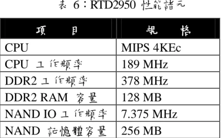
(32) 三、實驗與結果 3.1. 實驗帄台 為了驗證我們模擬器的準確性,我們使用圖 25 之 RTD2950系統晶片帄台 來比較實際硬體帄台效能測試的結果與模擬器輸出的效能結果差異。RTD2950 內建 NAND 快閃記憶體控制器存取 圖 26 為實驗帄台使用之快閃記憶體 Hynix HY27UF082G2B。RTD2950 的性能諸元,請見表 6。. 圖 25:RTD2950 實驗帄台. 圖 26:HY27UF082G2B 照片 . RTD2950 為 Realtek semiconductor 之液晶電視控制晶片,此論文發表之際尚未上市販售。 24.
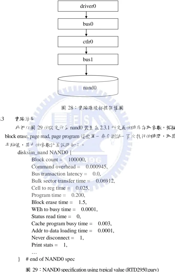
(33) 表 6:RTD2950 性能諸元 項. 規 格 CPU MIPS 4KEc CPU 工作頻率 189 MHz DDR2 工作頻率 378 MHz DDR2 RAM 容量 128 MB NAND IO 工作頻率 7.375 MHz NAND 記憶體容量 256 MB 3.2. 目. Disksim 環境設定 我們使用如圖 27 的設定作為系統拓撲設定,其示意圖如圖 28。 # system topology topology disksim_iodriver driver0 [ disksim_bus bus0 [ disksim_ctlr ctlr0 [ disksim_bus bus1 [ disksim_nand nand0 [] # end of bus1 ] # end of ctlr0 ] # end of bus0 ] # end of system topology ] 圖 27:實驗環境拓撲設定. 25.
(34) driver0 Driver0 bus0 ctlr0 bus1. nand0. 圖 28:實驗環境拓撲架構圖 3.3. 實驗結果 我們以圖 29 的設定作為 nand0 裝置在 2.3.1 所定義的時序存取參數,模擬 block erase, page read, page program 這些單一命令測試一百次執行的時間,取其 帄均值,其中的參數計算說明如:。 disksim_nand NAND0 { Block count = 100000, Command overhead = 0.000945, Bus transaction latency = 0.0, Bulk sector transfer time = 0.06912, Cell to reg time = 0.025, Program time = 0.200, Block erase time = 1.5, WEh to busy time = 0.0001, Status read time = 0, Cache program busy time = 0.003, Addr to data loading time = 0.0001, Never disconnect = 1, Print stats = 1, … } # end of NAND0 spec 圖 29:NAND0 specification using typical value (RTD2950.parv) 26.
(35) 1.. Command overhead = 3*(tCLS+tCLH)+4*(tWP+tWH) = 135 ns * 7 = 0.000945 ns. 2.. Bulk sector transfer time = 512*135 ns = 0.06912 ms. 3.. Status read time: 因為 RTD2950 的控制器支援 R/B 的狀態讀取,因此 不需額外花費時間發出 read status 的命令,因此設為 0。 表 7:單一命令之模擬與實驗時間比較表. Command Block erase Page read (512 bytes) Page program (512 bytes). A. Disksim (ms) 1.501045 0.095065 0.270165. B. RTD2950 (ms) 1.324519 0.096593 0.259259. C. 誤差 11.76% 1.61% 4.04%. 表 7 說明 Disksim 與實驗帄台量出的數據差異。其誤差原因主要在於快閃 記憶體 specifications 所載明之數據主要有一定程度之誤差。例如:我們以邏輯 分析儀量測這其中最重要的R/B忙碌時間[20]即與規格不同,而且這些值為典 型值,不一定每次均與規格書相同或接近,比較表如表 8。 表 8:Busy time 比較表 Command Block erase Page read (512 bytes) Page program (512 bytes). 典型值[20] (ms) 1.500000 0.025000 0.200000. 實測值 (ms) 1.322000 0.021200 0.183020. 為了修正誤差值,我們以表 8 的實測值重新定義,如圖 30。使用 Disksim 模擬,可得表 9 之A行結果。 disksim_nand NAND0 { Block count = 100000, Command overhead = 0.000945, Bus transaction latency = 0.0, Bulk sector transfer time = 0.06912, Cell to reg time = 0.0212, Program time = 0.18302, . 誤差之計算是以公式 C=abs(B-A)/A 27.
(36) }. Block erase time = 1.322, WEh to busy time = 0.0001, Status read time = 0, Cache program busy time = 0.003, Addr to data loading time = 0.0001, Never disconnect = 1, Print stats = 1, Max queue length = 1, … # end of NAND0 spec. 圖 30:NAND0 specification using measured value (RTD2950_fix.parv) 表 9:更新參數後之模擬與實驗時間比較表 Command Block erase Page read (512 bytes) Page program (512 bytes). A. Disksim (ms) 1.323045 0.091265 0.253185. B. RTD2950 (ms) 1.324519 0.096593 0.259259. C. 誤差 0.11% 5.84% 2.40%. 我們分析 Page read 仍有較大的誤差原因在於:使用 Disksim 模擬時,並 未加計軟體的運算時間,而在 RTD2950 上測得的數值包含設定控制器與讀取 計時器的軟體運算時間,此部份難以排除。由於 Page read 所耗時間相對地少, 所以前述之軟體運算時間所佔比例便相對地提高了。 不過另一做法是將驗證帄台的軟體運算時間加至 Disksim 的 iodriver 模 擬,這樣也可以改善誤差,進而提高本研究的精確度。. 28.
(37) 四、結論 Disksim 在研究儲存系統效能上被廣泛運用,而且被證明是精確、彈性、 有效率的工具。我們沿用其既有之架構、功能,加入快閃記憶體的裝置與控制 器模組,除了保有其優點外,使其功能支援 NAND 快閃記憶體儲存系統,並在 一系統晶片帄台驗證其基本命令的正確性。本研究之彈性設計即使不同的控制 器、記憶體也能適用,並可隨著新世代記憶體演進之規格而擴充,提高其可用 性。 經過實驗證明,實際硬體帄台效能測試的結果與模擬器輸出的效能結果差 異在 5.84% 以內,因此本研究可以作為快閃記憶體儲存系統研究(例如:FTL, Flash 檔案系統研究)的實驗與效能評估帄台。. 29.
(38) 參考文獻. [1] T. Bisson, S. A. Brandt and D.E. Long, “NVCache: Increasing the Effectiveness of Disk Spin-own Algorithms with Caching,” Proceedings of the 14th IEEE International Symposium on Modeling, Analysis and Simulation of Computer and Telecommunication Systems, 2006. MASCOTS 2006. 14th IEEE International Symposium on, pp. 422 - 432, 11-14 Sept. 2006. [2] Y. Hu, T. Nightingale and, Q. Yang, “Rapid-Cache: -A Reliable and Inexpensive Write Cache for High Performance Storage Systems,” IEEE Transactions on Parallel and Distributed System, Volume 13, No. 3,: pp. 290 - 307, March Mar. 2002. [ 3 ] Q. Zhu and Y. Zhou, “Power-aware Storage Cache Management,” IEEE Transactions on Computers, Volume 54, No. 5, pp. 587- 602, May 2005. [4] G. Memik, M. T. Kandemir and A. Choudhary, “Design and Evaluation of Smart Disk Architecture for DSS Commercial Workloads,” Proceedings of the International Conference on Parallel Processing, pp. 335 - 342, 21-24 Aug. 2000. [5] Y. Zhang, Sudhanva S. Gurumurthi and M. R. Stan, “SODA: Sensitivity Based. Optimization of Disk Architecture”, Proceedings of the Design Automation Conference, pp. 865 – - 870, 4-8 June Jun. 2007. [6] J. S. Bucy, Jiri J. Schindler, Steven S. W. Schlosser and , Gregory G. R. Ganger, “The Disksim Simulation Environment Version 4.0 Reference Manual”, http://www.pdl.cmu.edu/PDL-FTP/DriveChar/CMU-PDL-08-101.pdf, 2008. [7 ] R. Bez, E. Camerlenghi, A. Modelli and A. Visconti. “Introduction to Flash Memory,” Proceedings of the IEEE, Vol. 91, No. 4, pp.489- 502, Apr. 2003. [8 ]. Numonyx. Semiconductor. NAND. flash. memory. datasheet,. http://www.numonyx.com/Documents/Datasheets/NAND01GWxA2B-KGD.pdf, 2008 [9] E. Gal and S. Toledo, “Algorithms and Data Structures for Flash Memories,” ACM Computing Surveys, Vol. 37, No. 2, pp. 138-163, Jun. 2005. [10] NTFS File System, http://www.ntfs.com, 2008. 30.
(39) [11] C. H. Wu , T. W. Kuo, “An Adaptive Two-Level Management for the Flash Translation Layer in Embedded Systems,” Proceedings of the IEEE International Conference on Computer-Aided Design, pp. 601 - 606, Nov. 2006. [12] J. Kim, J. M. Kim, S. H. Noh, S. L. Min and Y. Cho, “A Space-Efficient Flash Translation Layer for Compact-Flash Systems,” IEEE Transactions on Consumer Electronics, Vol. 48, No. 2, pp. 366 – 375, May 2002. [13] Ban, “Flash File System”, U.S. Pat. No. 5,404,485, Apr 1995. [14] Ban, “Flash File System Optimized for Page-mode Flash Technologies”, U.S. Pat. No. 5,937,,425, Aug 1999. [15] Intel Corporation, “Understanding the Flash Translation Layer(FTL) Specification”, available at http://www.embeddedfreebsd.org/Documents/Intel-FTL.pdf, Dec 1998. [16] Intel Corporation, “FTL Logger Exchanging Data with FTL Systems”, available at http://www.myembed.com/down_list/005009/7510.htm, Aug 1995. [17] S. E.Wells, “Method for Wear Leveling in a Flash EEPROM Memory. US patent 5,341,339. Filed November 1, 1993; Issued August 23, 1994; Assigned to Intel. [18] M-systems Corporation, “Tow Technologies Compared: NOR vs. NAND White Paper”,. available. at. http://www.dataio.com/pdf/NAND/MSystems/MSystems_NOR_vs_NAND.pdf, Jul 2003. [19] Samgsung Electroncis, NAND Flash Memory Datasheet and SmartMedia Data Book, http://www.samsung.com/global/business/semiconductor/products/flash/Products_Fl ash.html, 2008. [ 20 ]. Numonyx. Semiconductor. NAND. flash. memory. datasheet,. http://www.hynix.com/datasheet/pdf/flash/HY27UF(08_16)2G2A(Rev0.4).pdf, 2008. [ 21 ]. Numonyx. Semiconductor. NAND. flash. memory. datasheet,. http://www.numonyx.com/Documents/Datasheets/NAND02G-B2D.pdf, 2008.. 31.
(40)
數據
![表 1:NAND/NOR 快閃記憶體比較表[ 18 ]](https://thumb-ap.123doks.com/thumbv2/9libinfo/8387695.178545/10.892.146.817.110.943/表1NANDNOR快閃記憶體比較表18.webp)
![圖 2:NAND 快閃記憶體存取界面示意圖[20] 圖 3:NAND 快閃記憶體存取界面訊號說明[20] 近來 SSD (Solid-State Drive) 快速崛起,在筆記型電腦及個人電腦的應用也 愈來愈廣泛,其中使用的就是快閃記憶體。我們預期,以半導體技術生產的快 閃記憶體儲存媒介未來會在儲存系統佔有一定的比例。因為快閃記憶體的特性 與限制與傳統磁碟不同,近來以快閃記憶體為基礎的儲存系統之相關研究開始 興盛。然而,如前所述,即使 Disksim 已在磁碟系統的研究領域有卓越成就, 可是](https://thumb-ap.123doks.com/thumbv2/9libinfo/8387695.178545/11.892.237.682.120.811/人電腦一定比例因為快閃記憶體的特性與限制與傳統磁碟不來以可是.webp)

+7
![圖 13:Address Latch Cycle [20]](https://thumb-ap.123doks.com/thumbv2/9libinfo/8387695.178545/24.892.172.731.173.834/圖-address-latch-cycle.webp)
![圖 14:Sequential Out Cycle after Read[20]](https://thumb-ap.123doks.com/thumbv2/9libinfo/8387695.178545/25.892.149.666.94.306/圖-sequential-out-cycle-after-read.webp)
![圖 17:Block Erase Timing[20]](https://thumb-ap.123doks.com/thumbv2/9libinfo/8387695.178545/26.892.157.776.119.906/圖-block-erase-timing.webp)
![圖 18:Status Read Timing[20]](https://thumb-ap.123doks.com/thumbv2/9libinfo/8387695.178545/27.892.161.801.285.996/圖-status-read-timing.webp)
相關文件
besides, data for the second quarter of 2010 have been re-compiled accordingly to facilitate direct comparison. Visitor Expenditure Survey and Visitors' Comments Survey
To Us Leaving Senior High School Life. Suddenly, we are about to graduate
Recycling Techniques are Available to Address Specific Pavement Distress and/or Pavement Structural Requirement.. Introduction to Asphalt Introduction
In Paper I, we presented a comprehensive analysis that took into account the extended source surface brightness distribution, interacting galaxy lenses, and the presence of dust
哈佛大學教授夏爾(Jeanne Chall)1983 年曾以六個階段描述兒童學習 閱讀的歷程,這六個階段又可分成兩大部份,分別是: 「學習如何讀」(learn to read ),「透過閱讀學習知識」(read to
• But, If the representation of the data type is changed, the program needs to be verified, revised, or completely re- written... Abstract
Discovering the City by Mining Diverse and Multimodal Data Streams – IBM Grand Challenge: New York City 360. § Exploring and Integrating Multiple Contents and Sources for
• When the coherence bandwidth is low, but we need to use high data rate (high signal bandwidth). • Channel is unknown
