國
立
交
通
大
學
電機學院 IC 設計產業研發碩士班
碩
士
論
文
平面顯示器玻璃基板上具有位階轉
換功能之類比輸出級電路設計
Design of Analog Output Buffers with Level
Shifting Function on Glass Substrate for Panel
Application
研 究 生:陳紹岐
指導教授:柯明道 教授
平面顯示器玻璃基板上具有位階轉
換功能之類比輸出級電路設計
Design of Analog Output Buffers with
Level Shifting Function on Glass
Substrate for Panel Application
研 究 生:陳紹岐 Student :Sao-Chi Chen
指導教授:柯明道 Advisor :Ming-Dou Ker
國 立 交 通 大 學
電機學院 IC 設計產業研發碩士班
碩 士 論 文
A Thesis
Submitted to College of Electrical and Computer Engineering National Chiao Tung University
in partial Fulfillment of the Requirements for the Degree of
Master in
Industrial Technology R & D Master Program on IC Design
July 2008
Hsin-Chu, Taiwan, Republic of China
平面顯示器玻璃基板上具有位階轉換功能之
類比輸出級電路設計
學生: 陳 紹 岐 指導教授: 柯 明 道 教授
國立交通大學
國立交通大學電機學院產業研發碩士班
摘要
低溫複晶矽(low temperature poly-silicon, LTPS)薄膜電晶體(thin-film transistors, TFT) 已被視為一種材料廣泛地應用於可攜帶式系統產品中,例如數位相機、行動電話、個人 數位助理(PDA) 、筆記型電腦等等,這是由於低溫複晶矽薄膜電晶體的電子遷移率 (electron mobility)約是傳統非晶矽(amorphous silicon)薄膜電晶體的百倍大。此外,低溫
複晶矽技術可藉由將驅動電路整合於顯示器面板之週邊區域來達到輕薄、小巧且高解析 度 的 顯 示 器 。 這 樣 的 技 術 也 將 越 來 越 適 合 於 系 統 整 合 型 面 板 (system-on-panel /system-on-glass)之實現。 近年來,低溫複晶矽技術具有將所有控制與驅動電路整合入玻璃基板的趨勢。一般 而言,液晶顯示器的驅動電路包含閘極驅動電路、資料驅動電路以及直流對直流轉換電 路。其中,資料驅動電路則是由移位暫存器、閂鎖器、電位移轉器、數位類比轉換器以
及類比輸出緩衝器所組成。然而,在量產線上仍無法精確控制複晶矽薄膜電晶體之晶粒 大小與晶粒邊界的一致性,這會使得複晶矽薄膜電晶體因為元件特性變化而具有較差的 一致性。元件特性的變化對於在液晶顯示面板上的類比電路設計是一個嚴重的問題。也 由於這個原因,在本論文中將著重於資料驅動電路中的類比電路設計。 在本篇論文中,提出了一個著重於元件特性變化考量之資料驅動電路的類比輸出緩 衝器,並以此緩衝器為基礎提出兩個具有位階轉換功能的類比輸出級電路,以上電路皆 以 3-m LTPS 製程技術實現。類比緩衝器可以在 100 kHz 的方波輸入訊號下具有 0.8 V 至 9 V 的輸出範圍。此具有位階轉換功能的類比輸出級電路也與數位類比轉換電路整合 在一起。可以藉由電路本身的位階轉換功能,在不需要修改驅動電路的前提下可驅動不 同工做電壓之面板,並且符合該面板所需的珈瑪補償曲線。
Design of Analog Output Buffers with Level Shifting
Function on Glass Substrate for Panel Application
Student: Shao-Chi Chen Advisor: Prof. Ming-Dou Ker
Industrial Technology R & D Master Program of
Electrical and Computer Engineering College
National Chiao-Tung University
ABSTRACT
Low temperature poly-silicon (LTPS) thin-film transistors (TFTs) have been widely
investigated as a material for portable systems, such as digital camera, mobile phone, personal
digital assistants (PDAs), notebook, and so on, because the electron mobility of LTPS TFTs is
about 100 times larger than that of the conventional amorphous silicon TFTs. Furthermore,
LTPS technology can achieve slim, compact, and high-resolution display by integrating the
driving circuits on peripheral area of display. This technology will also become more suitable
for realization of system-on-panel/system-on-glass (SOP/SOG) applications.
Recently, LTPS technology has a tendency towards integrating all control circuits and
driver circuits on the glass substrate. In general, the liquid-crystal display (LCD) driver
contains gate driver, data driver, and DC-DC converter. The gate drive usually utilizes high
voltage to enhance the response time of LCD monitor. The data driver is composed of shifter
However, the poly-Si TFTs suffered poor uniformity with large variations on the device
characteristics due to the narrow laser process window for producing large-grained poly-Si
TFTs. The device variation becomes a very serious problem for analog circuit design on LCD
panel. For this reason, the analog circuits of the data driver are focused in my works.
In this thesis, an on-panel analog output buffer for data driver with consideration of
device characteristic variation and output buffers with level shifting function are proposed in a
3-m LTPS technology. The proposed analog output buffer can be operated at 100 kHz rail-to-rail square wave input with a 0.8-to-9 V output swing. The proposed output buffer with
level shifter can be integrated with the digital-to-analog converter (DAC). This circuit can
誌謝
兩年的碩士生涯很快就過去了,在這兩年之中,首先最要感謝的是我的指導教授, 柯明道教授的殷殷教誨,在研究上他給予我們許多的自由、指導與建議,引導我們發揮 自己的創意及構想,還提供我相當多的資源,讓我能不斷地的充實自我;教導我們做事 情要抱持嚴謹的態度,待人處事要圓融等,平常也會關心我們的生活狀況,讓我獲益良 多。此外,由於老師的努力,讓我能有與業界合作與接觸的機會,也因此擁有了許多晶 片驗證的機會,在研究上不會有後顧之憂,另外,老師也常常為了修改我們的論文而廢 寢忘食。在此,我要向柯明道教授致上我最深的謝意,謝謝您讓我在碩士的兩年中能有 如此的成長。 在這段求學的過程中,『友達光電股份有限公司』給予我許多的研究的資源與幫助, 使我的電路能夠順利完成。在此特別感謝謝曜任處長、李純懷經理、郭俊宏副理、白承 丘、楊坤彥、李宇軒等諸位長官,在晶片下線與量測設備上,所給予我的許多幫助。 此外,我也要感謝『奈米晶片與系統實驗室』的陳榮昇、顏承正、張瑋仁、蕭淵文、 王資閔、林群祐、李宇軒、蒙國軒、莊介堯、黃曄仁、蔡佳琪、林彥良、翁怡歆、林佑 達、陳思翰等諸位實驗室學長姐以及學弟妹們,在各方面給予我許多幫助使我能順利完 成碩士論文。感謝『奈米晶片與系統實驗室』及助理卓慧貞小姐給予我在研究上的資源 及行政上的幫助,讓我完成學業。 接著要感謝的是一起打拼的同學們,小州哥、小胖、北鴨、小帆、99 範、科科、阿 宅、微笑阿邦、建名、宗恩、歐陽叔叔、歐威、國維以及塔哥,大家一起修課、熬夜、 看電影、聚餐、出遊,讓我的碩士生活多采多姿,大家在研究上互相討論、互相加油更 是碩士生涯中令我難忘的回憶;萬諶、維德、神童、豪哥、宗裕、舜哥、忠哥、松諭、 巧玲等等實驗室的學長姐,在學業上或其他方面上對我的幫助。 最後我要謝謝我的父親陳平護、母親魏如好、哥哥陳春陽以及女友逸雯,給予我一 切的支持與協助,使我無後顧之憂,在我失去信心時給我的支持與鼓勵,未曾對我失去 過信心。你們一直都是我精神上最大的支柱以及困難時的避風港。 還要感謝很多人,不可勝數,在此一併謝過,我不會讓你們失望的。 陳 紹 岐 僅誌於竹塹交大 民國九十七年七月CONTENTS
ABSTRACT(CHINESE) ... i
ABSTRACT ... iii
ACKNOWLEDGEMENT ... v
CONTENTS ... vi
TABLE CAPTIONS ... viii
FIGURE CAPTIONS ... ix Chapter 1 Introduction ... 1 1.1 BACKGROUND ... 1 1.2 MOTIVATION ... 1 1.3 THESIS ORGANIZATION ... 3 Chapter 2 Background Knowledge of Thin-Film Transistor Liquid Crystal Displays ... 7
2.1 LIQUID CRYSTAL DISPLAY STRUCTURE ... 7
2.1.1 Material and Display Theory of Liquid Crystal [4], [5] ... 7
2.1.2 Liquid Crystal Display Module Structure ... 9
2.1.3 Equivalent Model of Dot in each Pixel Cell ... 9
2.2 DRIVING METHOD IN TFT-LCD PANEL ... 11
2.2.1 Driving Method ... 11
2.2.2 Gamma Correction ... 12
2.3 PERIPHERY CIRCUIT BLOCK ... 13
2.3.1 Scan Driver Circuit ... 13
2.3.2 Data Driver Circuit ... 14
Chapter 3 An On-Panel Analog Output Buffer for Data Driver ... 24
3.1 INTRODUCTION ... 24
3.2 DEVICE CHARACTERISTIC VARIATION IN LTPS TECHNOLOGY ... 25
3.3 ON-PANEL ANALOG OUTPUT BUFFER ... 26
3.31 Source Follower Analog Output Buffer [16], [17] ... 26
3.3.2 Unity-Gain Output Buffer with an OPAMP [18]... 26
3.4 EXPERIMENTAL RESULTS ... 28
3.5 DISCUSSION ... 29
Chapter 4
The Analog Output Buffers with Level Shifting Function for DAC ... 43
4.1 INTRODUCTION ... 43
4.2 DIGITAL-TO-ANALOG CONVERTERS [19]-[23] ... 43
4.2.1 R-String DAC with Switch Array Decoding ... 44
4.2.2 R-String DAC with Binary Tree... 44
4.2.3 R-String DAC with Digital Decoding ... 44
4.2.4 Charge-Redistribution DAC ... 44
4.2.5 Resistor-Capacitor Hybrid DAC ... 45
4.2.6 Current-Steering DAC ... 46
4.3 ANALOG OUTPUT BUFFER with LEVEL SHIFTING FUNCTION ... 47
4.3.1 Analog output buffer with level shifting function type I ... 47
4.3.2 Analog output buffer with level shifting function type II ... 48
4.4 EXPERIMENTAL RESULTS ... 49
4.5 DISCUSSION ... 49
4.6 SUMMARY ... 50
Chapter 5 Conclusion and Future Works ... 67
5.1 CONCLUSION ... 67
5.2 FUTURE WORKS ... 68
REFERENCES ... 69
TABLE CAPTIONS
Table 3.1 The mobility variation for n-type and p-type TFTs at different stress conditions ... 30 Table 3.2 Summary of the simulated circuit performances of the output buffer in
Fig. 3.8 ... 30 Table 3.3 The total measurement results of the unity-gain output buffer ... …31 Table 4.1 The comparisons of six kinds of the digital-to-analog converter circuits
... …..51 Table 4.2 The resistance of R2 in 0~63 Gray Level ... …51 Table 4.3 The resistance of the analog output buffer with level shifting function type
I ... 52 Table 4.4 The resistance of the analog output buffer with level shifting function type
FIGURE CAPTIONS
Fig. 1.1 System integration roadmap of LTPS TFT-LCD. ... 4
Fig. 1.2 A CPU with an instruction set of 1-4bity and 8-bit data bus on glass substrate. ... 4
Fig. 1.3 Basic concept of pixel memory technology. ... 5
Fig. 1.4 The roadmap of LTPS technologies leading toward the realization of sheet computers. ... 5
Fig. 1.5 (a) Comparison of an amorphous silicon TFT-LCD module and (b) a low-temperature polycrystalline silicon TFT-LCD module. ... 6
Fig. 2.1 Phase of liquid crystal materials versus temperature. ... 15
Fig. 2.2 (a) A couple of polarizers with 90∘phase shift. (b) A couple of polarizers with liquid crystal. ... 15
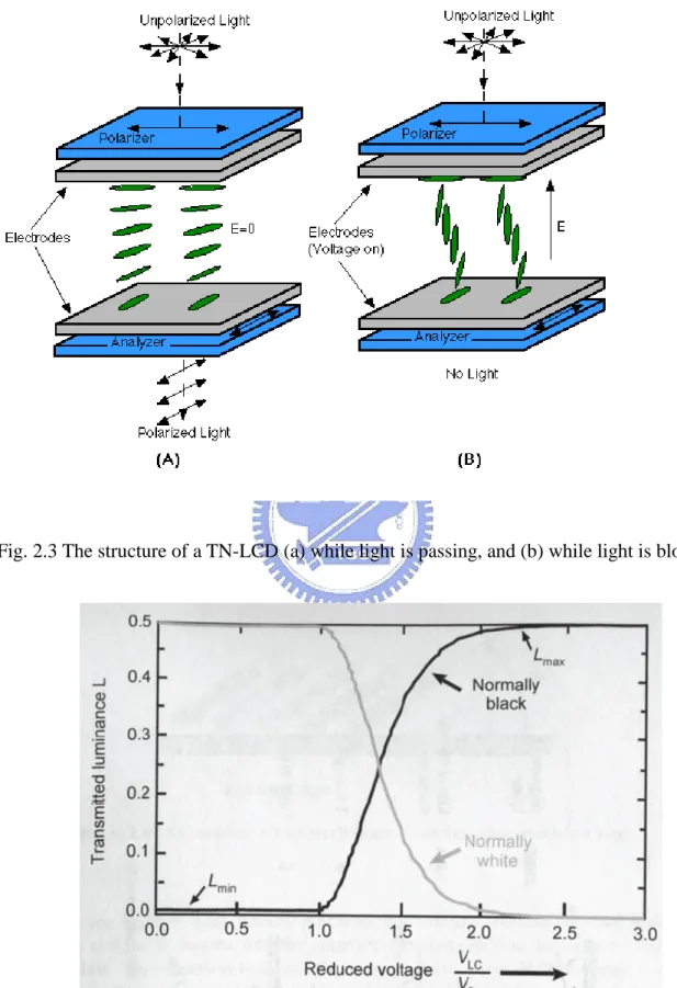
Fig. 2.3 The structure of a TN-LCD (a) while light is passing, and (b) while light is blocked. ... 16
Fig. 2.4 The transmitted luminance versus the normalized voltage (VLC/V0) across the LC cell for the normally white mode and the normally black mode. ... 16
Fig. 2.5 The cross section structure of TFT-LCD panel. ... 17
Fig. 2.6 The basic layout and cross section of an AMLCD sub-pixel. ... 17
Fig. 2.7 The equivalent circuit of a TFT in the sub-pixel with voltages, currents, and parasitic capacitances. ... 17
Fig. 2.8 The layout view of a TFT-LCD sub-pixel: (a) CS on common mode and (b) CS on gate mode. ... 18
Fig. 2.9 The equivalent circuit of a TFT-LCD sub-pixel: (a) CS on common mode and (b) CS on gate mode. ... 18
Fig. 2.10 The polarity inversions of TFT-LCD panel. ... 19
Fig. 2.11 The operation waveform of direct driving method. ... 20
Fig. 2.12 The operation waveform of AC modulation driving method. ... 20
Fig. 2.14 The input digital code vs. pixel voltage curve of data driver in TFT-LCD panel. ... 21
Fig. 2.15 The block diagram of the entire TFT-LCD panel circuits. ... 21
Fig. 2.16 The entire addressing system in detail. ... 22
Fig. 2.17 The basic diagram of scan driver circuit. ... 22
Fig. 2.18 The basic diagram of data driver circuit. ... 23
Fig. 3.1 The Variation on threshold voltage (VTH) of 120 LTPS n-type TFTs in different location on the LCD panel. ... 32
bias voltage. ... 32
Fig. 3.3 (a) The conventional source follower output buffer and (b) its output waveforms at different input voltage. ... 33
Fig. 3.4 The Monte Carlo simulation results of the conventional source follower output buffer... 33
Fig. 3.5 The source follower output buffer with a compensation capacitor. ... 34
Fig. 3.6 The source follower output buffer compensation by device matching (a) the circuit schematic and control signal (b) the measurement results. .. 34
Fig. 3.7 The output unity-gain buffer with OPAMP. ... 35
Fig. 3.8 The two-stage OPAMP with p-type TFTs input circuit. ... 35
Fig. 3.9 The simulation results of analog output buffer with p-channel input. .. 36
Fig. 3.10 The die photo of analog output buffer with p-channel input in 3-m LTPS process. ... 36
Fig. 3.11 The measurement setup of frequency response. ... 37
Fig. 3.12 The measurement procedure of unity-gain frequency. ... 37
Fig. 3.13 The unity-gain bandwidth measurement results of unity-gain buffer with OPAMP. ... 38
Fig. 3.14 The measurement setup of large signal (rail-to-rail square wave ). ... 38
Fig. 3.15 The output waveform of large signal measurement at 100k Hz input signal (a) the pulse width of output waveform is larger than 1/4 period. (b) the pulse width of output waveform is smaller than 1/4 period. ... 39
Fig. 3.16 The measurement results of large signal. ... 39
Fig. 3.17 The offset voltage measurement setup of unity-gain buffer. ... 40
Fig. 3.18 The measurement of offset voltage when vi is 2.5V. ... 40
Fig. 3.19 The measurement of offset voltage when vi is 5V. ... 41
Fig. 3.20 The measurement of offset voltage when vi is 7.5V. ... 41
Fig. 3.21 (a) Circuit and signal-timing diagram of the analog output buffer with the offset compensation technique. (b) The measurement result of this analog output buffer with the offset compensation technique under 50-kHz square wave with a swing of 2-to-8 V. ... 42
Fig. 4.1 The 6-bit R-string DAC with switch array decoding. ... 53
Fig. 4.2 A 3-bit R-string DAC with binary-tree decoding. ... 53
Fig. 4.3 The R-string DAC with digital decoding. ... 54
Fig. 4.4 The charge-redistribution DAC. ... 54
Fig. 4.5 The resistor-capacitor hybrid DAC. ... 55
Fig. 4.6 The current-steering DAC. ... 55
Fig. 4.7 Two gamma curves of different panels. ... 56
Fig. 4.8 The level change circuit by SHARP. ... 56
Fig. 4.10 The noninverting amplifier circuit with variable resistor. ... 57 Fig. 4.11 Total circuit of analog output buffer with level shifting function type I.……
... 58 Fig. 4.12 The decoder1 in analog output buffer with level shifting function type I.
... ……58 Fig. 4.13 The decoder2 in analog output buffer with level shifting function type I.
... ……59 Fig. 4.14 The operation method of analog output buffer with level shifting function
type I when the Din is “000100”. ... 59 Fig. 4.15 The simulation results of analog output buffer with level shifting function
type I. ... 60 Fig. 4.16 The noninverting amplifier with an amendment voltage. ... 60 Fig. 4.17 The value of the amendment voltage (Va). ... 61 Fig. 4.18 Total circuit of analog output buffer with level shifting function type II.
... ……61 Fig. 4.19 The decoder2 of analog output buffer with level shifting function type
II.… ... 62 Fig. 4.20 The operation method of the output buffer with level shifting function type
II, when Din is “001000”. ... 62 Fig. 4.21 The simulation results of analog output buffer with level shifting function
type II. ... 63 Fig. 4.22 The die photo of output buffer with level shifting function type I. ... 63 Fig. 4.23 The die photo of output buffer with level shifting function type II. ... 64 Fig. 4.24 The measurement setup of analog output buffer with level shifting
function type I. ... 64 Fig. 4.25 The measurement setup of analog output buffer with level shifting
function type II. ... 65 Fig. 4.26 The measurement results of analog output buffer with level shifting
function type II. ... 65 Fig. 4.27 The measurement result of analog output buffer with level shifting
function type II. ... 66 Fig. 5.1 To reduce the power system of analog output buffers with level shifting
Chapter 1
Introduction
1.1 B
ACKGROUNDAt present, active matrix liquid crystal display (AMLCD) is a huge industry in Taiwan,
because AMLCD panel is an important part in many electronic products. We can know that
the revenue of LCD industry in Taiwan is over one trillion NT dollars in 2007. Not only the
large size LCD TV, the small and middle size LCD market are also in growth now. For
portable application we need low power, slim and lighter weight. But between panel and
display driving circuit has many interconnects in conventional amorphous silicon (a-Si)
thin-film transistors (TFTs) technology. In order to reduce the size and cost down, a new
technology is needed.
1.2
M
OTIVATIONHowever, the low field-effect mobility (ability to conduct current) of amorphous silicon
(a-Si) thin-film transistor (TFT) slows their application only as pixel switching device. There
temperature they can withstand. The process of high-temperature poly-Si TFTs has a problem
in expensive quartz substrate. Low temperature poly-silicon (LTPS) TFTs had been widely
used in active matrix liquid crystal display (AMLCD), because electron mobility can be 100
times faster than that of the conventional amorphous silicon (a-Si) TFTs. Many small-sized to
mid-sized AMLCDs fabricated by LTPS technology have been used in mobile phone, digital
camera, personal digital assistants (PDAs), notebook, and so on. The state-of-the-art design
efforts focus on realization of system-on-panel/system-on-glass (SOP/SOG) application to
integrate more control and driver circuits on the glass substrate. Fig1.1 shows the system
integration roadmap of LTPS TFT-LCD [1].
System-on-panel (SOP) displays are value-added displays with various functional
circuits. For example, a CPU with an instruction set of 1-4 bytes and an 8bit data bus on glass
substrate is shown in Fig. 1.2 [2]. The static random access memory (SRAM) also has been
integrated in each pixel as Fig. 1.3 [1]. When SRAMs and a liquid crystal AC driver are
integrated in a pixel area under the reflective pixel electrode, the LCD is driven by only the
pixel circuit to display a still image. It means that no charging current to the data line for a
still image. Fig. 1.4 shows the roadmap of LTPS technologies leading toward the realization
of sheet computers. Finally, all of the necessary function will be integrated in LTPS
TFT-LCD [3].
The distinctive feature of the LTPS TFT-LCD is the elimination of TAB-ICs (integrated
circuits formed by means of an interconnect technology known as tape-automated bonding).
LTPS TFTs can be used to manufacture complementary metal oxide semiconductors (CMOSs)
in the same way as in crystalline silicon metal oxide semiconductor field-effect transistors
(MOSFETs). The PCB connection pads are thus reduced to one-twentieth the size of those in
a-Si TFT-LCDs. The most common failure mechanism of TFT-LCDs, disconnection of the
a high-resolution display because the TAB-IC pitch (spacing between connection pads) limits
display resolution to 130 ppi (pixels per inch). A higher resolution of up to 200 ppi can be
achieved by LTPS TFT-LCDs. Therefore, the SOP technology can effectively relax the limit
on the pitch between connection terminals to be suitable for high-resolution display.
Furthermore, eliminating TAB-ICs allows more flexibility in the design of the display system
because three sides of the display are now free of TAB-ICs [3]. Fig. 1.5 shows a comparison
of a-Si and LTPS TFT-LCD modules.
1.3
T
HESISO
RGANIZATIONChapter 2 introduces background knowledge of thin-film transistor liquid crystal
displays, liquid crystal display structure in TFT-LCD, panel, driving method of TFT-LCD and
periphery circuit block. The nonlinear relationship between luminance, human visual system
(HVS), and gamma correction method will be discussed in this chapter.
In chapter 3, an analog output buffer fabricated in 3-m LTPS process is proposed. The device character variation of LPTS process has been discussed in this chapter. The design of
analog output buffer had considered with the device variation.
In chapter 4, we will talk about digital-to-analog converter (DAC) circuit and proposed
analog output buffers with level shifting function. Simulation results and measured results
about analog output buffers with level shifting function are shown in this chapter.
Fig. 1.1 System integration roadmap of LTPS TFT-LCD [1].
Fig. 1.3 Basic concept of pixel memory technology [1].
Fig. 1.4 The roadmap of LTPS technologies leading toward the realization of sheet computers [3].
Fig. 1.5 (a) Comparison of an amorphous silicon TFT-LCD module and (b) a low-temperature polycrystalline silicon TFT-LCD module.
Chapter 2
Background Knowledge of Thin-Film Transistor
Liquid Crystal Displays
2.1
L
IQUIDC
RYSTALD
ISPLAYS
TRUCTURE2.1.1 Material and Display Theory of Liquid Crystal [4], [5]
Liquid crystal is a phase of matter whose order is intermediate between that of a liquid
and that of a crystal. Fig. 2.1 shows the phase variation of liquid crystal in different
temperature. Most liquid crystals consist of molecules shaped like the rod. Rod-shaped
molecules are referred to as calamitic. Calamitic (Bahaur, 1990; Demus et al., 1998a,b) liquid
crystal has many applications. One characteristic of the phase variation of liquid crystal
materials is ―the twice melting‖ showing in Fig. 2.1. Below the melting point (Tm) they are solid, crystalline and anisotropic, when above the clearing point (Tc) they are clear and
isotropic liquid. The material has the appearance of a milky liquid between Tc and Tm but still
exhibit the ordered phases.
The phases during Tc and Tm can roughly be divided into smectic phase and nematic
phase by its molecules arrangement. The molecules are ordered in two dimensions in smectic
nematic phase is the basis and widely used as Twisted Nematic (TN) cell with active matrix
addressing. Because the twist of liquid crystals can be controlled by the electric field that is
applied across it, liquid crystals are used as a switch that passes or blocks the light.
The polarizer can block or pass the specific light by changing the phase of the polarizer.
In general, the first polarizer of a couple of polarizers is called polarizer and the second
polarizer of these is called analyzer. The light can be blocked by a couple of polarizers with
90° phase shift, is shown in Fig. 2.2 (a). If we twist the liquid crystal molecule by applying
the specific electric field across it, the light still can pass the polarizer. This is because the
direction of liquid crystal molecules varies with electric field and it can guide the light along
the long axis, shown in Fig. 2.2 (b).
Fig. 2.3 (a) shows a pixel of a transmissive twisted nematic LC-cell with no voltage
applied. The white backlight f passes the polarizer. The light leaves it linearly polarized in the
direction of the lines in the polarizer, and passes the glass substrate, the transparent electrode
out of Indium-Tin-Oxide (ITO) and the transparent orientation layer. In this case, the analyzer
is crossed with polarizer. The light can pass the analyzer without applied voltage due to the
twisted nematic LC-cell and the pixel appears white. If a voltage VLC of the order of 10 V is
applied across the cell, as shown in Fig. 2.3 (b), all molecules aligned parallel to the electric
field. In this state, the wave that reaches the crossed analyzer is polarized in the same
direction as at the input. Therefore, the analyzer blocks the light and the pixel appears black.
This operation is termed the normally white (NW) mode. On the contrary, if the analyzer is
rotated by 90°, paralleled with polarizer, the light is blocked in the analyzer. The pixel is black.
This is called the normally black (NB) mode. The transmitted luminance, also termed
transmittance, of the light. Fig. 2.4 shows the transmitted luminance versus the normalized
voltage (VLC/V0) across the LC cell for the normally white mode and the normally black
2.1.2 Liquid Crystal Display Module Structure
The cross section structure of TFT-LCD panel is shown in Fig. 2.5 particularly. It can be
roughly divided into two part, TFT array substrate and color filter substrate, by liquid crystal
filled in the center of LCD panel. We still need a backlight module including an illuminator
and a light guilder since liquid crystal molecule cannot light by itself. However it usually
consumes the most power of the system, some applications such as mobile communications
try to exclude or replace it from the system. In TFT array substrate, we need a polarizer, a
glass substrate, a transparent electrode and an orientation layer. In color filter substrate, we
also need an orientation layer, a transparent electrode, color filters, a glass substrate and a
polarizer. Most transparent electrodes are made by ITO, and they can control the directions of
liquid crystal molecules in each pixel by voltage supplied from TFT on the glass substrate.
Color filters contain three original colors, red, green, and blue (RGB). As the degree of light,
named ―gray level‖, can be well controlled in each pixel covered by color filer, we will get more than million kinds of colors.
2.1.3 Equivalent Model of Dot in each Pixel Cell
One dot is the most fundamental unit of LCD panel and each dot can express one kind of
original color. Because one full color should be mixed with three original colors, each pixel
composed of three dots. Fig. 2.6 shows the basic layout and cross section of the AMLCD
sub-pixel. The equivalent circuit of a TFT sub-pixel with voltages, currents, and parasitic
capacitances is shown as Fig. 2.7 [4].
Fig. 2.8 and Fig. 2.9 show the layout and equivalent circuit of each sub-pixel, including
two major structures, the CS on common mode and CS on gate mode. The right-down region
of the sub-pixel layout is the TFT switch, and the region of each sub-pixel area excluding TFT
light passing. So the larger ratio of aperture region to pixel area is the better performance of
the TFT-LCD panel. In Fig. 2.9, the MS is a thin film transistor as a switch. The Clc is the
effective capacitor of liquid crystals, and CS is the storage capacitor used to maintain the
voltage level of liquid crystals during the hold time of frame transitions. The Cgd is the
parasitic capacitor between gate line and effective liquid crystal capacitor. The structure, CS
on gate, which connects the bottom of the storage capacitor to the previous row of the gate
line has some benefits. By this structure, we can compensate the unstableness of voltage level
due to the clock feed-through effect from Cgd. Furthermore, this structure also has larger
aperture ratio. But the trade-off with the CS on gate method is an increase in the RC time
2.2
DRIVING
METHOD
IN
TFT-LCD
PANEL
2.2.1 Driving Method
Liquid crystal molecules can‘t be under a fixed voltage in the long period. The DC blocking effect and the DC residue (stick image) will be appeared under this condition.
Therefore, the electric field polarity should be inversed every period to avoid the destruction
of liquid crystals. The torque caused by electric filed is dependent on the magnitude of
electric filed, not dependent on the polarity of electric filed. Therefore, the polarity of electric
filed would not affect the twisting of the liquid crystal molecules. When the frame picture will
be kept on the same gray level, the electric field across liquid crystals is changed into two
polarities (positive and negative), alternately. As electric field is higher than common mode
voltage the polarity is called positive polarity, otherwise it is called negative polarity. By this
way, the liquid crystal molecules will avoid defection in the fixed applied voltage. In term of
above description, the polarity inversions of LCD panel can be principally divided into four
general types: frame inversion, row inversion, column inversion, and dot inversion [6]. They
are listed in Fig. 2.10. Frame inversion is that all the adjacent pixels of the LCD panel have
the same polarity. Row inversion (column inversion) is that each adjacent row pixels (adjacent
column pixels) have different polarity. Finally, all the adjacent pixels of LCD panel have
different polarity is called dot inversion. Dot inversion is the major driving method of LCD
panel. This polarity inversion method has some benefits. By this method, we can achieve
higher quality image due to the reduction in both horizontal and vertical cross-talk. The
flicker of image also can be reduced due to the spatial averaging of pixels. But the penalty of
dot inversion method is an increase of the power consumption due to the line inversion
Based on the operational type of common mode voltage, the driving method can also be
classified into direct driving and AC modulation driving. Fig. 2.11 and Fig. 2.12 show these
two driving methods. Direct driving method would keep its common voltage on a constant
level. However, the common mode voltage of AC modulation driving method is not a constant
level, is a period voltage. The characteristics of two driving methods are listed below:
Direct driving method:
– Frame, row, column, and dot inversion are all available. – Crosstalk and flicker can be eliminated.
AC modulation driving method:
– Frame and row inversion are available. – Low power dissipation in data driver.
2.2.2 Gamma Correction
Gamma correction of liquid crystal displays is involved due to the nonlinearity between
luminance and human visual system (HVS). This is because the pupils of the human‘s eyes would vary automatically for the change of the ambient light. For this reason, a data driver
with gamma correction is necessary in TFT-LCD panel. The data driver often is required to
compensate for the human visual system‘s transfer function. Moreover, it must also compensate for the LCD transfer function [6]. Fig. 2.13 shows the operation of the gamma
correction for the normally white TN type LCD panel. The gamma correction system is
composed of three relationships: luminance vs. HVS brightness, input digital code vs. pixel
voltage, and the V-T curve of the NW-TN type liquid crystal. By this system, the relationship
2.3 P
ERIPHERYC
IRCUITB
LOCKThe periphery circuit blocks of LCD panel are roughly composed of four parts — display
panel, timing control circuit, scan driver circuit and data driver circuit [10]. In Fig. 2.15 is the
block diagram of the entire TFT-LCD panel circuits. Display panel is constructed of the active
matrix liquid crystals. The operation of the active matrixes is similar to DRAM (dynamic
random access memory) which is used to charge and discharge the capacitor of the pixel.
Timing controller is responsible for transiting RGB (red, green, and blue) signals to the data
driver and controlling the behavior of scan driver. As soon as one voltage level of the scan
lines rises, the RGB signals will be transited through the data driver. After a period, the
voltage level of this scan line will be disabled and next scan line will be turned on. All voltage
levels of those scan lines will be raised in turn. Addressing system, in Fig. 2.16, is composed
of scan driver and data driver [4]. These two driver circuits will be further discussed in the
following sections.
2.3.1 Scan Driver Circuit
Scan driver, shown in Fig. 2.17, consists of shifter register, level shifter, and digital
output buffer. Shifter register is used to store digital input signals and transit them to the next
stage according to timing clock. Because the turn-on voltage of active matrixes is higher, scan
driver should drive the active pixels with a high voltage. The purpose of the level shifter is
just to convert the digital signals to a higher level voltage. Finally, since the scan lines can be
modeled as RC (resister and capacitor) ladder, the digital output buffer should be used in the
2.3.2 Data Driver Circuit
Data driver, shown in Fig. 2.18, mainly contains shifter register, data latch, level shifter,
digital-to-analog converter (DAC) and analog output buffer [7]. Furthermore, the first three
parts classify as digital architectures. The other two parts belong to analog architectures.
Shifter register and data latch manage to transit and store the RGB signals. Also, the purpose
of level shifter is the same as the one in scan driver. It is applied to translate the RGB signal to
a higher level voltage. As implied by the name, digital-to-analog converter is used to convert
the digital RGB signal to analog gray level. Its structures can be divided into many types, and
there will be much more detailed discussion in the next chapter. As for analog output buffer,
its purpose is applied to drive active pixels into a desired gray level. However, The LCD panel
usually has large loading, especially in larger panel display or higher resolution display. For
this reason, the analog output buffer should enhance the driving capability of the data driver.
Fig. 2.1 Phase of liquid crystal materials versus temperature.
Fig. 2.2 (a) A couple of polarizers with 90∘phase shift. (b) A couple of polarizers with liquid crystal.
Fig. 2.3 The structure of a TN-LCD (a) while light is passing, and (b) while light is blocked.
Fig. 2.4 The transmitted luminance versus the normalized voltage (VLC/V0) across the LC cell
Fig. 2.5 The cross section structure of TFT-LCD panel.
Fig. 2.6 The basic layout and cross section of an AMLCD sub-pixel.
Fig. 2.7 The equivalent circuit of a TFT in the sub-pixel with voltages, currents, and parasitic capacitances.
(a) (b)
Fig. 2.8 The layout view of a TFT-LCD sub-pixel: (a) CS on common mode and (b) CS on gate mode.
Fig. 2.9 The equivalent circuit of a TFT-LCD sub-pixel: (a) CS on common mode and (b) CS on gate mode.
Fig. 2.11 The operation waveform of direct driving method.
Fig. 2.14 The input digital code vs. pixel voltage curve of data driver in TFT-LCD panel.
Fig. 2.16 The entire addressing system in detail.
Chapter 3
An On-Panel Analog Output Buffer for Data Driver
3.1
I
NTRODUCTIONWe know that the LTPS TFTs have been widely investigated as a material for portable
systems, like mobile phone, personal digital assistants (PDAs), digital camera, and so on. The
electron mobility of LTPS TFTs is about 100 times larger than the electron mobility of
conventional amorphous silicon TFTs, so LTPS can integrate driving circuit on panel and
smaller pixel transistor. Display of LTPS TFTs technique can achieve slim, compact, and
high-resolution. The system on panel (SOP) will be realized if the electron mobility of poly-Si
continuity increased in the future. The CPU, memory, and display will be integrated in one
panel by SOP technology [8], [9].
Now, the LTPS TFTs technology is toward integrating the driving circuits on the glass
substrate [10], [11]. In general, the driving circuits of display contain gate driver, data driver,
and DC-DC converter. The data driver contains shift register, latch, level shifter,
digital-to-analog converter (DAC), and analog output buffer. DAC and analog output buffer
are the region of analog circuit. Analog output buffer is proposed in this chapter. The output
buffer design is critical to achieve low power dissipation, high resolution, and large output
3.2
D
EVICEC
HARACTERISTICV
ARIATIONI
NL
TPST
ECHNOLOGYAlthough the electron mobility of LTPS TFTs is larger than that of conventional a-Si
TFTs, LTPS TFTs technology confront by the variation of device characteristic. The LTPS
process can enlarge poly-grain size to improve the device performance, but the electron
mobility across the grain boundary is various and gate-insulator interface defect. The LTPS
devices have a random device-to-device variation on LCD panel. Fig. 3.1 shows the variation
on threshold voltage (VTH) of 120 LTPS n-type TFTs in different locations on the LCD panel
[12]. The distribution of VTH is from 0.75 V to 2.15 V [12]. Fig. 3.2 shows the device
characteristic variation of LTPS p-type TFTs in different gate bias voltage [13]. Based on
these figures, we know that the variation of LTPS technology is larger than the variation of
CMOS technology. In real products, LTPS technology is limited in small size panel. Because
the LTPS TFTs technology has poor uniformity and large variation on the device
characteristics due to the narrow laser process window for producing the large-grained
poly-Si thin film. The grain boundaries exist in the channel randomly. This causes the
non-uniformity brightness in the panels, current or voltage gain mismatching in analog
circuits and error reading in digital circuits [14]. Based on these reasons, the variation of
device characteristic becomes an important issue of the design for analog circuit in LTPS
TFTs technology [15]. In this work, an analog output buffer with consideration of device
3.3 O
N-P
ANELA
NALOGO
UTPUTB
UFFER3.31 Source Follower Analog Output Buffer [16], [17]
Source follower output buffer is the most common pattern integrated on the glass
substrate for data driver. Source follower can be an output buffer because it has high input
impedance and low output impedance, but there are some drawbacks like low output swing
and higher input offset voltage. Fig. 3.3 shows the circuit of conventional source follower
output and its output waveforms at different input voltage. From this figure, we can find that
there is always an offset voltage between input voltage and output voltage. The value of offset
voltage is the threshold voltage of TFT. Besides, the threshold voltage is not a constant in
different panel location. The Monte Carlo simulation results of source follower output buffer
is shown in Fig. 3.4. Even though the source follower output buffer has a threshold voltage
offset, there are many ways of compensation technique to compensate the offset voltage. Like
Fig. 3.5 shows, it uses the switches, a capacitor and control signals to reduce the offset
voltage. Fig. 3.6 (a) shows the other technique, this circuit only used switching transistors to
eliminate the offset voltage. The simulation results and measurement results are shown as Fig.
3.6 (b).
3.3.2 Unity-Gain Output Buffer with an OPAMP [18]
Compared with source follower output buffer, unity-gain output buffer with OPAMP has
lower offset and better output swing range. The relation function between the input voltage
and output voltage of unity-gain buffer with OPAMP is
𝑉𝑜𝑢𝑡 = 𝐴
The unity-gain output buffer with OPAMP is shown as Fig. 3.7. In this work, the two-stage
OPAMP is adopted as a unity-gain buffer. Two-stage OPAMP has high open-loop gain, large
output swing, and medium bandwidth.
A class-A two-stage OPAMP with P-type TFTs input circuit schematic as Fig. 3.8 shows.
When the output node (Vout) is connected with the negative input node (Vin-), there is a
unity-gain buffer with OPAMP circuit. The class-A OPAMP with p-type TFTs input circuit is
composed of four parts. The first part is composed of a p-type differential pair (M1-M2),
current mirror load (M3-M4) and current source (M5). It is the input stage and it provides
gain to OPAMP. The second part is a common-source stage and active load (M6-M7) which is
the output stage. The third part is constant-Gm bias stage (M11-M16 and RB) which can
provide the bias voltage for this circuit. Constant-Gm bias circuit produces a
supply-independent current for the first and second parts. The fourth part is a start-up circuit
(M21-M24) which turns on the bias circuit in the beginning and turn off automatically after
bias circuit works. In this circuit, the Miller compensation capacitor and null resistor (Cc and
M10) are adopted as frequency compensation, which provide a pole and a zero.
Based on Table 3.1 [13], the variation of p-type TFTs in LTPS process is smaller than the
variation of n-type TFTs in LTPS process. The differential pair is the most important part in
the OPAMP circuit. The variation of input stage device has large influence on the performance
of OPAMP. That is the reason for using p-type TFTs input in OPAMP circuit. Fig. 3.9 shows
3.4 E
XPERIMENTALR
ESULTSThe class-A output buffers with p-type input stage has been designed and fabricated in
3-m LTPS process. Fig. 3.10 shows the photograph of a class-A output buffer with p-type TFTs input stage. The measurement setup is as Fig. 3.11shown. Tektronix TDS 3054 is an
oscilloscope using to detect and display the signal waveforms. HP 8116 Pulse/Function
Generator is function generator which can provide input signals, like square wave form or
sine waveform. The programmable power supply (GW PPT-1630 GPIB) can provide three
independent voltage sources.
The measurement procedure of unity-gain frequency is shown as Fig. 3.12. When the
input frequency rises up, the output waveform will suffer a gain pick. After the gain pick, the
output waveform will be smaller as frequency rise up. Fig.3.13 shows the unity-gain
bandwidth measurement results. The numbers in the figure bars are the number of samples.
Fig. 3.14 shows the measurement of large signal input. The large signal means the rail-to-rail
square wave. Fig. 3.15 shows the output waveform of large signal input. The measurement
results of large signal input are shown in Fig. 3.16. The offset voltages of the unity-gain buffer
had been measured as Fig. 3.17. We give the input a DC voltage and measurement the output
voltage by meter. The measurement of offset voltage is shown in Fig. 3.18, Fig. 3.19 and Fig.
3.5 D
ISCUSSIONThe accuracy of the data driver is determined by DAC circuit combined with analog
output buffer. Even though the DAC has high accuracy, the data driver also does not have
enough accuracy with a low accuracy analog output buffer. For this reason, the input offset
voltage of the analog output buffer will become a serious issue in data drivers. Fig. 3.21
shows a valid input offset compensation method and the measurement results of this analog
output buffer with the offset compensation technique [12]. During the period I, the offset
voltage is stored in CH. In the period II, the detected offset voltage in CH is added into the
inverting input node. From Fig. 3.21 (b), we can find that the offset voltage of this analog
output buffer can be compensated under the second period by using this offset compensation
technique.
3.6 S
UMMARYIn this chapter, a class-A output buffer with pTFT-pair as input stage to suppress device
variation in LTPS technology has been proposed and fabricated in a 3-μm LTPS technology.
The output buffer with P-TFTs input stage can be operated at 100-kHz operation frequency
with about 0.8-to-9 V output swing under AVDD of 10 V and GND of 0 V. The offset voltages
are less than 150 mV in three different input voltage conditions. The device characteristic
variation has been successfully suppressed by replacing the critical part of analog circuits by
the P-TFTs. The proposed output buffer with P-TFTs input stage can be used in the on-panel
data drivers to provide a uniform brightness and high resolution display. Furthermore, this
proposed analog output buffer is also suitable for ambient light sensor system to boost the
Table 3.1 The mobility variation for n-type and p-type TFTs at different stress conditions [13]
Average Variation (%) Std. Dev Hot-Carrier Stress Condition N-Type -38.627 6.65 P- Type +7.054 2.72 On-Current Stress Condition N- Type +11.828 3.28 P- Type +2.251 0.6525
Table 3.2 Summary of the simulated circuit performances of the output buffer in Fig. 3.8
Open Loop Characterization Gain 55.09 dB Phase Margin 114˚ Unity-gain Bandwidth 1.83 MHz CMRR 58.3 dB Close Loop Characterization PSRR AVDD 57.3 dB PSRR GND 50 dB Output Swing @50kHz 0.81~9.72 V Slew Rate L to H 1.29 V/s Slew Rate H to L 2.22 V/s
Table 3.3 The total measurement results of the unity-gain output buffer Sample Number Output Swing Range (V) @100k Hz Maximum Operation Frequency under Sinusoidal Wave Input
(Hz) Maximum Operation Frequency under Rail-to-Rail Square Wave Input (Hz) Offset Voltage (mV) Simulation 0.7~9.6 1.82M 70K - 01 0.4-9.6 2.1M 190k 50~110 02 0.28-9.4 1.9M 210k 1100~1260 03 0.44-9.5 3M 200k 30~90 04 0.2-9.1 2.7M 210k 110~190 05 0.4-9 2.4M 240k 40~90 06 0.2-8.8 2.2M 180k 10~50 07 0.2-8.8 2.3M 230k 20~90 08 0-9.6 2M 210k 10~70 09 0-10 2.3M 300k 0~90 10 0-8.6 1.2M 150k 10~90 11 0-8.6 900k 100k 1300~1460
Fig. 3.1 The Variation on threshold voltage (VTH) of 120 LTPS n-type TFTs in different location
on the LCD panel [12].
Fig. 3.2 The device characteristic variation of LTPS p-type TFTs in different gate bias voltage [13].
Fig. 3.3 (a) The conventional source follower output buffer and (b) its output waveforms at different input voltage.
Fig. 3.5 The source follower output buffer with a compensation capacitor.
Fig. 3.6 The source follower output buffer compensation by device matching (a) the circuit schematic and control signal (b) the simulated and measurement results [17].
Fig. 3.7 The unity-gain output buffer with OPAMP.
Fig. 3.9 The simulation results of analog output buffer with p-channel input.
Fig. 3.10 The die photo of analog output buffer with p-type TFTs input stage in a 3-m LTPS process.
V
iV
oAVDD
GND
C
CM6
M1
M2
M7
R
BAVDD = 10 V
Fig. 3.11 The measurement setup of frequency response.
Fig. 3.13 The unity-gain bandwidth measurement results of unity-gain buffer with OPAMP.
Fig. 3.15 The output waveform of large signal measurement at 100k Hz input signal (a) the pulse width of output waveform is larger than 1/4 period. (b) the pulse width of output waveform is smaller than 1/4 period.
Fig. 3.17 The offset voltage measurement setup of unity-gain buffer.
Fig. 3.19 The measurement of offset voltage when vi is 5V.
Fig. 3.21 (a) Circuit and signal-timing diagram of the analog output buffer with the offset compensation technique. (b) The measurement result of this analog output buffer with the offset compensation technique under 50-kHz square wave with a swing of 2-to-8 V [21].
Chapter 4
The Analog Output Buffers with Level Shifting
Function for DAC
4.1
INTRODUCTIONBased on Chapter 2, we know that the data driver of LCD is composed of shift register,
latch, level-shifter, DAC, analog output buffer. In small size application, some requirements
are claimed to drive different voltage level LCD panels without changing the DAC. It is the
feature of analog output buffers with level shifting function. In this chapter, we will describe
the DAC circuit, and analog output buffers with level shifting function. An OPAMP had been
proposed in chapter 3. OPAMP is an important part of analog output buffers with level
shifting function.
4.2
D
IGITAL-T
O-A
NALOGC
ONVERTERS[19]-[23]
Digital-to-analog converter (DAC) circuit is a basic part of LCD data driver which
analog gray level voltage of DAC circuit and charges the loading capacitor to the same
voltage which it senses. There are some common kinds of DAC circuits as follow:
4.2.1 R-String DAC with Switch Array Decoding
Fig 4.1 shows the 6-bit R-string DAC with switching array decoding circuit. This circuit
is widely used in most of LCD data driver, because this architecture requires no digital
decoder and suitable for gamma correction design. This circuit can be easy layout in the sides
of panel. However, the area of switches becomes larger and larger due to the high resolution
DAC. The output node (Vout) loading becomes larger due to the huge switch array.
4.2.2 R-String DAC with Binary Tree
Fig. 4.2 shows a 3-bit R-string DAC with binary-tree decoding. The R-string DAC with
binary-tree decoding has less transistors compare with R-string DAC with switch array
decoding. But in the high resolution, this architecture becomes larger and larger in the
decoding circuit. The loading of output node (Vo) also becomes larger because of the
binary-tree decoder.
4.2.3 R-String DAC with Digital Decoding
The R-string DAC with digital decoding is shown as Fig. 4.3. Compare with last two
architectures, the digital decoder can reduce the loading of output node (Vo). The area of
digital decoder still becomes larger and larger in high resolution DAC. And the decoder also
becomes more complex in high resolution DAC. This architecture of DAC circuit is usually
used in high speed applications.
replace the input capacitor of a switched-capacitor (SC) gain amplifier by programmable
capacitor array (PCA) of binary-weighted capacitors. In this circuit, it has two phases. In first
phase (φ1), all capacitor bottom plates are connected to a reference voltage and top plates are connected to ground. During second phase (φ2), capacitor bottom plates are connected to a
reference voltage or ground according to logic high or logic low in codes. By this operation,
the voltage level in output terminal can be determined by a formula which is shown in follow:
𝑉𝑜 = 𝑉𝑟𝑒𝑓 × 𝐶 2𝑁𝐶 + 𝐶 𝑝 × 𝑏𝑖2 𝑖 𝑁−1 𝑖=0 (2) Where bi is the bit number in input code, N is the total bit number and Cp is top plate parasitic
capacitance. This circuit structure has some advantages better than the resistor-string DAC.
First, the process matching for capacitor is better than resistor string. Second,
charge-redistribution DAC can save more power because it has no DC path in the circuit.
However, it has a big problem in LCD panel application. That is, this method is very difficult
to achieve gamma correction. In other word it cannot compensate the inherent characteristic
of liquid crystal.
4.2.5 Resistor-Capacitor Hybrid DAC
The benefits and drawbacks of resistor-string DAC and charge-redistribution DAC have
been discussed previously. In order to get their benefits and exclude the drawbacks in the
DAC, a hybrid structure has been proposed in Fig. 4.5. In this circuit, the upper bits are
adopted in resistor-string architecture and the lower bits are employed the
charge-redistribution structure. There are two phases in this circuit operation. In first phase
(φ1), all capacitor bottom plates are connected to ground. During second phase (φ2), capacitor bottom plates are connected to a reference voltage V1 or connected to the other reference
voltage V2 which is according to logic high or logic low in input codes. Furthermore, a
𝑉𝑜 = 𝑉𝑟𝑒𝑓 2𝑀 × 𝑏𝑖+𝐿2𝑖 𝑀−1 𝑖=0 × 1 2𝑀 × 𝑉𝑟𝑒𝑓 2𝐿 × 𝑏𝑗2𝑗 = 𝑉𝑟𝑒𝑓 2𝑁 × 𝑏𝑖2𝑖 (3) 𝑁−1 𝑖=0 𝐿−1 𝑗 =0
Where M is the total bit number in resistor-string DAC, L is the total bit number in
charge-redistribution DAC and N is the total bit number in this DAC (N = M + L).
This hybrid structure can achieve high performance in operational speed, die area, and
power consumption. Besides, it is also suitable in gamma correction DAC.
4.2.6 Current-Steering DAC
Current-steering DAC is very similar to resistor-based converter, but is intended for
higher-speed application due to the current type. The basic idea is to switch currents to either
the output or to ground, as shown in Fig. 3.8. Here, the total output current is sum of the
currents which are selected, as shown below:
𝐼𝑜 = 𝐼 × 𝑏𝑁−1 × 2𝑁−1+ 𝑏
𝑁−2× 2𝑁−2+ ⋯ + 𝑏1× 21 + 𝑏0× 20 (4)
This output current is converted to a voltage through a resistor (RF). Although, this circuit has
potentially large glitches due to timing skews and the monotonicity in this DAC is not
guaranteed. But, we can reduce the glitches and provide the guaranteed monotonicity by using
the thermometer decoding method.
From previous description and analysis, we can summarize a table about many kinds of
the DAC circuits, as shown in Table 4.1. In this table, we can clearly find the characteristics
of those DAC, like: suitable for gamma correction design, operation speed, power
4.3 A
NALOGO
UTPUTB
UFFERwithL
EVELS
HIFTINGF
UNCTIONIn general, a DAC circuit is only suitable to drive one kind of panel. Therefore, we have
an idea that one DAC circuit to drive multi panels. As shows in Fig. 4.7, there are two gamma
curves. We had a DAC for 3V panel and fit its gamma curve. Now we need a circuit to level
shift the voltage to fit the gamma curve of 5V panel. Sharp had published a circuit which has
such ability. As Fig. 4.8 shows, Sharp called this circuit ―level change circuit‖ [24].
4.3.1 Analog output buffer with level shifting function type I
The basic idea here is a noninverting amplifier as Fig. 4.9 [22]. Even if the gain of the
OPAMP is large in Fig. 4.9, the function of this noninvertin amplifier is shown in below:
Vout = Vin 1 +R1
R2 (5) When the R2 of this noninverting amplifier is a vary-resistor, the circuit will be like Fig.4.10.
Table 4.2 shows the resistance of R2 in different Gray Level. But the variable resistor can‘t be
fabricated in the integrated circuit. The R-string with switching array has the same capability.
As shown in Fig. 4.11, we use the R-string and switching array to achieve variable resistor in
the total circuit. The DAC for 3V panel is composed of RS00~RS64, MS01~MS64 and
decoder1. The R201~237 and MR01~MR37 achieve the variable resistor R2. The structure of
OPAMP is a differential input single output operator amplifier that we had proposed in
chapter 3. The circuit of OPAMP is show as Fig. 3.8. But the power supply of the OPAMP
becomes 0-to-6V. The decoder1 of this circuit is a digital decoder as shown in Fig. 4.12. The
output Do101~Do164 are the delegate of the 64 gray levels. When the input signal (Din) is a
6-bit signal, one of the outputs (Do101~Do164) will be in logic ―1‖. The decoder2 is also a
Do201~Do237. As Fig. 4.13 shows, the principle of decoder2 is using the input signal
(Do101~Do164) which represent the Gray level to choose the R2 value.
The operation method is shown as Fig. 4.14. When the digital input signal (Din) is
―000100‖. The output Do105 of decoder1 will be in logic ―1‖, and MS105 will turn on. The voltage value of Vin+ and Vin- will be as V4. In decoder2, the Do205 will be in logic ―1‖.
MR205 will turn on. The output voltage is shown in below:
𝑉𝑜𝑢𝑡 = 𝑉4 × 1 + 𝑅1
𝑅201 + 𝑅202 + 𝑅203 + 𝑅204 + 𝑅205 (6) The resistance value of output buffer with level shifter is shown in Table 4.3. The simulation
results are shown in Fig. 4.15.
4.3.2 Analog output buffer with level shifting function type II
Moreover, we have another idea to level shift the 3V gamma curve to 5V gamma curve.
The basic idea is also a noninverting amplifier, but the R2 is a constant resistance as Fig. 4.16
shown. The Va is an amendment voltage. The function of this circuit is shown in below:
𝑉𝑜𝑢𝑡 = 𝑉𝑖𝑛 × 1 +𝑅1
𝑅2 − 𝑉𝑎 𝑅1
𝑅2 (7) The value of amendment voltage Va is shown as Fig. 4.17 when the resistance of R1is equal
to the resistance of R2. We achieve the Va by R-string and decoder2. The total circuit
schematic is shown as Fig. 4.18. The DAC for 3V panel is composed of RS00~RS64,
MS01~MS64 and decoder1. The RA01~RA30, MA01~MA29 and decoder2 achieve the
amendment voltage Va. The resistance of RA01~RA30 are list in Table 4.4. Fig.4.19 shows
the decoder2 circuit schematic of analog output buffer with level shifting function type II. The
decoder1 of output buffer with level shifting function type II is the same as the decoder1 of
output buffer with level shifting function type I. The operation method is like the output
4.4 E
XPERIMENTALR
ESULTSFig. 4.22 shows the photograph of the output buffer with level shifting function type I.
The measurement setup is shown as Fig. 4.24. The photograph of analog output buffer with
level shifting function type II is as Fig. 4.23 shown. Fig 4.25 shows the measurement setup of
analog output buffer with level shifting function II. The programmable power supply (GW
PPT-1630 GPIB) can provide three independent voltage sources. The voltage value of node
with FPC PAD (Vout, Vin+, and Vin-) can be measured by the multimeter ( HP 34401A
MULTIMETER). The digital signal input (Din) achieve by bread board and manual
switching.
The measured results of analog output buffer with level shifting function type I are
shown in Fig. 4.26. The measured results of analog output buffer with level shifting function
type II are shown as Fig. 4.27
4.5 D
ISCUSSIONThe differences in voltage value between the measured results of analog output buffer
with level shifting function type I and idea value are from 10 to 300 mV. But the differences
in voltage value between the measured results of analog output buffer with level shifting
function type II and idea value are from 10 to 70 mV. Compare with the measured results of
analog output buffer with level shifting function type II, the measured results of analog output
buffer with level shifting function type I are worse. The reason is that the layout of R-String
of analog output buffer with level shifting function type II has been modified after measuring
4.6 S
UMMARYAccording to the measured results of the two analog output buffers with level shifting
function, the function of them are correct. Two kinds of analog output buffer with level
shifting function have been proposed and fabricated in a 3-m LTPS process. They also contain the DAC circuit with gamma correction in the circuit. Therefore, these two analog
Table 4.1 The comparisons of six kinds of the digital-to-analog converter circuits
Type Correction Speed Power Area Complexity
R-String DACs with Switch Array Decoding
Best Poor Normal Poor Easy
R-String DACs with Binary Tree
Best Normal Normal Normal Easy
R-String DACs with Digital Decoding
Best Good Normal Normal Medium
Charge-Redistribution DAC Poor Good Best Normal Medium
Resistor-Capacitor Hybrid DAC
Good Good Good Good Hard
Current-Steering DAC Poor Best Poor Normal Hard
Table 4.2 The resistance of R2 in 0~63 Gray Level
Gray Level Resistance (k) Gray Level Resistance (k) Gray Level Resistance (k) Gray Level Resistance (k) 0 90 16 456 32 613 48 635 1 106 17 472 33 620 49 635 2 145 18 483 34 620 50 620 3 183 19 496 35 635 51 620 4 211 20 508 36 635 52 620 5 241 21 519 37 635 53 613 6 268 22 531 38 640 54 606 7 294 23 541 39 640 55 596 8 317 24 550 40 640 56 596 9 337 25 560 41 645 57 587 10 359 26 570 42 645 58 570 11 376 27 579 43 645 59 560 12 398 28 587 44 645 60 550 13 411 29 596 45 640 61 541 14 427 30 598 46 640 62 531 15 442 31 606 47 635 63 483
![Fig. 1.2 A CPU with an instruction set of 1-4bity and 8-bit data bus on glass substrate [2]](https://thumb-ap.123doks.com/thumbv2/9libinfo/8434141.181400/17.892.136.790.155.521/fig-cpu-instruction-set-bity-data-glass-substrate.webp)
![Fig. 1.4 The roadmap of LTPS technologies leading toward the realization of sheet computers [3]](https://thumb-ap.123doks.com/thumbv2/9libinfo/8434141.181400/18.892.143.781.125.941/fig-roadmap-ltps-technologies-leading-realization-sheet-computers.webp)
![Table 3.1 The mobility variation for n-type and p-type TFTs at different stress conditions [13]](https://thumb-ap.123doks.com/thumbv2/9libinfo/8434141.181400/43.892.116.805.185.404/table-mobility-variation-type-tfts-different-stress-conditions.webp)
![Fig. 3.2 The device characteristic variation of LTPS p-type TFTs in different gate bias voltage [13]](https://thumb-ap.123doks.com/thumbv2/9libinfo/8434141.181400/45.892.146.749.633.1055/fig-device-characteristic-variation-ltps-tfts-different-voltage.webp)
![Fig. 3.6 The source follower output buffer compensation by device matching (a) the circuit schematic and control signal (b) the simulated and measurement results [17]](https://thumb-ap.123doks.com/thumbv2/9libinfo/8434141.181400/47.892.135.769.554.958/follower-compensation-matching-circuit-schematic-control-simulated-measurement.webp)
