國 立 交 通 大 學
光電工程研究所
博士論文
利用有機金屬氣相沈積法成長氮化鎵量子侷限
發光元件之研究
Research on Nitride-Based Quantum Confined Light
Emitting Device Grown By Metalorganic Chemical
Vapor Deposition System
研究生: 姚忻宏
Student: Hsin-Hung Yao
指導教授: 王興宗
郭浩中
Advisor: Shing-chung Wang
Hao-Chung Kuo
利用有機金屬氣相沈積法成長氮化鎵量子侷限
發光元件之研究
Research on Nitride-Based Quantum Confined Light
Emitting Device Grown By Metalorganic Chemical
Vapor Deposition System
研究生: 姚忻宏
Student: Hsin-Hung
Yao
指導教授:
王興宗
郭浩中
Advisor: Shing-chung
Wang
Hao-Chung Kuo
國立交通大學
光電工程研究所
博士論文
A dissertation
Submitted to Institute of Electro-Optical Engineering
College of Electrical Engineering and Computer Science
National Chiao Tung University
In Partial Fulfillment of the Requirements
For the Degree of
Doctor of Philosophy
In Electro-Optical Engineering
June 2006
Hsin-chu, Taiwan, Repubic of China
利用有機金屬氣相沈積法成長氮化鎵量子侷限
發光結構之研究
研究生:姚忻宏 指導教授:王興宗 教授
郭浩中 教授
國立交通大學光電工程研究所
摘要
氮化鎵材料由於擁有極寬的直接能隙結構及優異的材料特性,因此成功的開發出高 亮度之藍光、綠光和紫外光之短波長發光二極體,以及藍光雷射二極體等發光元件,成 為極具潛力之開發材料。為了發展下一世代的氮化鎵系發光元件以及提升元件之內部及 外部的量子效率,本論文在研究以有機金屬氣相化學沉積法(Metalorganic chemical vapor deposition, MOCVD)製作氮化鎵系量子侷限發光之結構。其中包括氮化鎵系半導 體微共振腔以及氮化銦鎵量子點等結構之開發。 在本研究中,為了製作高品質的氮化鎵系微共振腔結構,我們先發展氮化鎵系高反 射率布拉格反射鏡的結構。藉由設計和模擬布拉格反射鏡的結果,選擇了氮化鋁和氮化 鎵材料作為氮化鎵系的布拉格反射鏡的基材來減少布拉格反射鏡的層數和增加高反射 區域的寬度。本研究利用 MOCVD 技術成長高反射率的氮化鎵系布拉格反射鏡,以優化過 的磊晶參數以及不對稱的布拉格反射鏡結構,成功製作出不會崩裂的高反射率的氮化鎵 系布拉格反射鏡。 接著,利用發展出的高反射率氮化鎵系布拉格反射鏡為下反射鏡以及介電質氧化物 布拉格反射鏡為上反射鏡,我們成功製作出一個3 波長長度的高品質氮化鎵系微共振腔 結構。利用光激發的方式測試製作出來的氮化鎵系面射型雷射結構,已可成功在室溫下 觀測到激發輻射的雷射現象,其等效的臨界電流密度為 53mJ/cm2 ,證明微共振腔結構的 品質已達到要求。在元件開發上,我們也成功製做了電激發式的氮化鎵系微共振腔發光 元件,觀察到微共振腔對自發輻射的侷限效應並使其發光波長對注入電流有極高的穩定 性及較高的光輸出量子效率。 最後,我們成功的利用 MOCVD 成長了氮化銦鎵量子點結構並研究中斷成長對氮化銦 鎵量子點的效應。以優化過的磊晶參數成長氮化銦鎵量子點結構其量子點密度已可達到 4.5 × 1010 cm-2 且其量子點的平均側向大小為 11.5 奈米,平均高度為 1.6 奈米。研究結 果顯示中斷成長能調製量子點的大小尺寸及其發光波長。優化的中斷成長參數可以增加 量子點的密度和發光效率。對未來製作氮化銦鎵量子點的電激發式發光元件提供了良好 的基礎。Research on Nitride-Based Quantum Confined Light
Emitting Devices Grown By Metalorganic Chemical Vapor
Deposition
Student: Hsin-Hung Yao Advisor: Dr. Shing-Chung Wang
Dr. Hao-Chung Kuo
Institute of Electro-Optical Engineering National Chiao Tung University
Abstract
GaN materials are very interested for their direct wide bandgap structures and many advantages of material properties. Therefore they are likely to be the basis of a strong development of novel family semiconductor devices, for optronics as well as for electronics. Recently, III-V nitride semiconductors have been the commercial productions with a extremely wide applications; high brightness light emitting diodes (LEDs) emitting from green to near UV can be used as any kind of lighting, room-temperature violet laser light emission has paved the way to wider possibilities in optical storage, and high-power, high-temperature electronic devices have been used in harsh environments like automotive engines, space, and avionics.
In this study, in order to develop new generation device and to resolve some material issues on nitride-based light emitting devices, we have developed the optical and electric quantum confined structure grown by metal organic chemical vapor deposition (MOCVD). They are included the developments of GaN-based microcavity structures and InGaN Quantum dots (QDs) structure.
For the fabrication of high quality nitride-based microcavity structures, we started this study from design and simulation to obtain a high reflectance nitride-based distributed Bragg reflector (DBR) with a reasonable numbers of pair and stopband width in DBR structure. The monolithically grown AlN/GaN DBR structure has been demonstrated and the fabrication issues of AlN/GaN DBR structure have been resolved. By optimizing the growth condition and developing an non-quarterwave stacks DBR structure to control the accumulative strain energy, A high reflectance AlN/GaN DBR structure with crack-free surface have been successful growth.
Using the high reflectance AlN/GaN DBR as the bottom mirror, and a dielectric oxide DBR structure as the top mirror, we have fabricated a 3λ nitride-based microcavity with the hybrid DBR mirrors resonant structure. The feasibility of this nitride-based microcavity structure is examined by the performance of optical pumped, and the laser action has been achieved under the optical pumping at room temperature with a threshold pumping energy density of about 53 mJ/cm2. The nitride-based microcavity emits 448 nm with a linewidth of 0.25 nm. Following, the electrically driven device with nitride-based microcavity structure has been fabricated and the characteristics of the 3λ GaN-based microcavity light emitting device structures have been discussed. A much less red-shift with injection current and a higher output power caused by the resonance effect in this MCLED has been observed.
Finally, the electric quantum confined structure with a quantum dots (QDs) structure has also been grown and the characteristic were also been studied. We have grown a self-assembled InGaN QDs structure with the growth interruption by MOCVD. The density of InGaN QDs was about 4.5 × 1010 cm-2 with an average lateral size of 11.5 nm and an
optical properties were studied. The results suggested that the interruption growth could modify the size of InGaN QDs and extend the emission wavelength to the short wavelength region, and at the same time improve optical quality of the QDs.
致謝
博士論文的完成,對我來說意義非凡,是對自我的肯定,也代表著另一階段人生的 開始。自 1995 年高中畢業來到新竹,到 2006 年拿到博士學位,回想過去 11 年充實的 學習生活,真的是在許多人的教導、協助與鼓勵之下,才能如此順利的拿到我的博士學 位。 最要感謝指導老師王興宗教授在碩士、博士這七年期間的指導與教誨,讓我學習到 做學問的方法、精神及態度。老師在研究資源上的高度支持,及鼓勵學生積極參與國際 學術研討會的理念,促使學生的格局提高、眼界放寬,對我的人生有著很深的影響。想 起初進實驗室的莽撞與不成熟到能夠完成一本厚厚的博士論文,在此向王老師至上最高 的謝意與敬意。老師,謝謝您。 這些年來跟著實驗室一起成長,感謝實驗室學長姐和學弟妹的幫忙與討論,也感謝 郭浩中老師的指導,提升了我的研究的廣度;盧廷昌學長在成果發表的幫助,不厭其煩 的幫我修改論文,特此感謝。研究過程中,要感謝佳鋒學長的提攜與機台的教導,讓我 能夠順利進入氮化鎵長晶的研究領域;哲偉能夠在微共振腔元件草創時期勇敢扛下製成 的重責大任並漂亮的完成任務,在此時,我特別懷念三人一起奮鬥的那段日子,謝謝你 們。另外,也感謝最後加入的乃方學妹在數學模擬、理論計算的幫助,讓我能順利完成 論文最後的部分,也要感謝學妹在論文撰寫時期在各方面的支持,辛苦你了。 這段不算短的時間,感謝安琪學姐、維巍、昭遠、俊華和名芳這群在資格考一起唸 書的伙伴,能夠認識你們,是我博士班其間最珍貴的收穫,也是我的驕傲。還要感謝小 狐狸、名益、炎璋、褚立、亦中、哩哩、俞君、佩玲、金鍊、佐昀、瓊文、IRIS 等,讓 我的博士生活添加了許多色彩和歡樂。 最後,要感謝我親愛的父母親,姚培華先生與李榮嬌女士,你們全心全力的支持及 毫無怨言的付出,讓我能在沒有後顧之憂的情況下,克服求學路程上之顛簸,希望我讓 你們能感到絲毫的驕傲。 僅 以 此 論 文 獻 給 所 有 關心我 及 幫助我 的人 忻宏 于 95 年 6 月 24 日 交通大學光電所 謙虛卑恭,知足圓滿CONTENTS
Abstract (in Chinese) i Abstract ii Acknowledgement v Contents viList of tables viii
List of figures ix
CHAPTER 1
Introduction
1-1 Wide Bandgap Materials – Group III-Nitride
Semiconductors 1
1-2 Next Generation Devices 3
1-3 Vertical Cavity Light Emitting Devices 3
1-4 Quantum Dots Structures 6
1-5 Overview of this thesis 8
References 10
CHAPTER 2
Metalorganic Chemical Vapor Deposition
System
2-1 Reaction Equations 19
2-2 Gas Blending Systems 23
2-3 Reactor Chamber 24
2-4 Heating System 26
2-5 In-Situ Reflectance Monitoring During III-Nitrides
Growth 27
References 31
CHAPTER 3
Fabrication of the Nitride-Based Distributed
Bragg Reflector
3-1 Characteristics of Distributed Bragg Reflectors 48 3-2 Fabrication Issues of Nitride-based DBR structures 52 3-3 MOCVD Growth of AlN/GaN DBR Structures Under
Various Ambient Conditions 55
3-4 Suppression of Crack Generation in AlN/Gan
Chemical Vapor Deposition
References 67
CHAPTER 4
Characteristic of Nitride-Based Microcavity
Structure
4-1 Fabrication Process of Nitride-Based Microcavity Composed of Hybrid DBR Resonator 95 4-2 Characteristics of Optically Pumped Blue GaN-Based
Microcavity Structure 97
4-3 Fabrication Process of Nitride-Based Microcavity Light
Emitting Device 100
4-4 Characteristics of stable emission nitride-based microcavity light-emitting devices 102
References 105
CHAPTER 5
Self-Assembled InGaN Quantum Dots Grown
by MOCVD System
5-1 Introduction of Self-Assembled Nitride-Based
Quantum Dots 130
Effects of growth interruption on InGaN/GaN
self-assembled quantum dots grown by metal organic
chemical vapor deposition 132
References 142
CHAPTER 6
Conclusions and Future Works
Conclusions 162
Future Works 165
List of tables
Table 1-1 Comparison of features for EEL vs VCSEL.
14
Table 2-1 The names and properties of some of a the more commonly
used metalorganic (MO) compounds for III-V and II-VI MOCVD ”common” implies a widely used material.
33
Table 3-1 The boundary conditions of electric and magnetic fields at
each interface
70
Table 3-2 The arrangement of simulation result of DBR structure with
different index contrast.
74
Table 3-3 The arrangement of surface morphologies of DBR structure
grown under different ambient gases.
80
Table 3-4 Comparison of the experimental and simulated peak
reflectance values of these three 30-pair AlN/GaN distributed Bragg reflectors
82
Table 3-5 The necessary parameters to calculate strain energy in
AlN/GaN DBR structures.
87
Table 4-1 The parameters used in the estimation of threshold gain and
threshold carrier density.
115
Table 4-2 Initial Clean (I.C.) Process
119
Table 4-3 Detail process flowchart of nitride-based MCLED structure.
121
Table 5-1 The arrangement of AFM and PL measured
154
Table 5-2 The necessary parameters for simulation of InGaN QDs
structure
156
Table 5-3 The arrangement of analysis results for growth interruption
effect on InGaN QDs structure
160
List of figures
Chapter 1
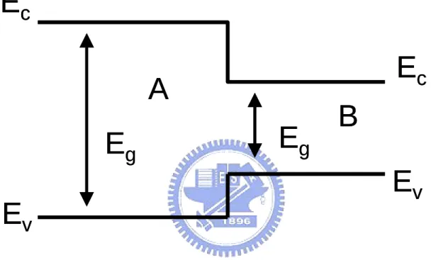
Figure 1-1 Energy band diagram for an ideal abrupt heterojunction
of type I between two different semiconductor materials labeled A and B.
13
Figure 1-2 The schematic diagram of nitride-based microcavity
structure
15
Figure 1-3 Three nitride-based microcavity structures: The
all-epitaxial mirrors resonator structure, one amorphous-dielectric mirrors resonator structure, and all-dielectric mirrors resonator structure.
16
Chapter 2
Figure 2-1 Schema of EMCORE D-75 system
34
Figure 2-2 Major components of a low pressure MOCVD system.
35
Figure 2-3 Components functions in a low pressure MOCVD
system
36
Figure 2-4 Schema of gas blending system in MOCVD.
37
Figure 2-5 Two types MOCVD systems (a) Vertical chamber, (b)
Horizontal chamber
38
Figure 2-6 Gas flow patterns for high speed rotating disk
39
Figure 2-7 Schema of reactor design in MOCVD D-75 system.
40
Figure 2-8 Picture of Filament used in EMCORE D-75
41
Figure 2-9 Model for the growth of GaN grown by MOCVD using
the LT-buffer layer
42
Figure 2-10 Schematic of in-situ monitoring configuration. By
collecting the reflection of a tungsten-Lamp light perpendicularly impinging on the wafer surface
43
sapphire.
Figure 2-12 The calibration of growth rate for different
nitride-based materials by in-situ reflectance measurement.
45
Figure 2-13 The schematic diagram of the controlling apparatus for
in-situ monitoring system.
46
Chapter 3
Figure 3-1 The schematic diagram of normal incidence on a single
dielectric layer.
69
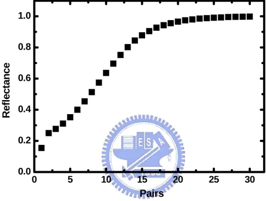
Figure 3-2 The simulation results for DBR structures with 5, 10,
20, and 30 pairs. The refraction indices of nH and nL are set as 2.4, and 2.1, respectively.
71
Figure 3-3 The peak reflectance of DBR structures with different
pair number.
72
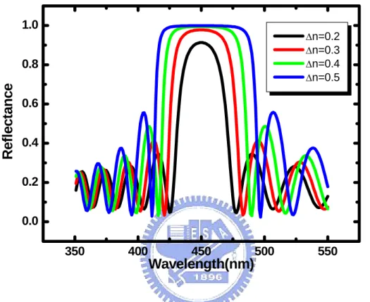
Figure 3-4 The simulation results for 20-pair DBR structures with
n=0.2, 0.3, 0.4, and 0.5, respectively.
73
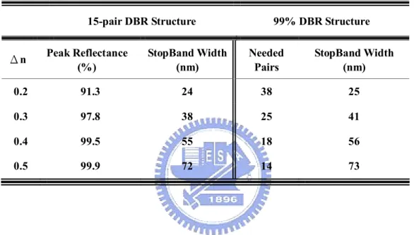
Figure 3-5 The simulation result of asymmetric DBR structure.
75
Figure 3-6 The arrangement of peak reflectance and stopband
width for different thickness ratio between these two composed materials of 20-pair DBR structure.
76
Figure 3-7 The schematic structures of a 30-pair AlN/GaN DBR.
77
Figure 3-8 The schematic of the reflectance measurement setup
with normal incidence at room temperature.
78
Figure 3-9 The surface morphologies of AlN/GaN DBR structure
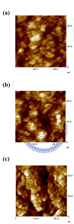
grown under (a) N2, (b) H2+N2, and (c) H2 ambient
gas.
79
Figure 3-10 Experimental optical reflectance spectra of three
30-pair AlN/GaN DBR (solid lines) and numerical simulations of the optical reflectance spectra (dash lines).
Figure 3-11 (a) Cross-section TEM image of sample A. The darker
layers are AlN while the lighter layers are GaN. (b) the layer images for sample A, B, and C.
83
Figure 3-12 The arrangement of thickness of AlN and GaN layers
in these three DBR samples.
84
Figure 3-13 In situ normal reflectance measurement during the
growth of the Bragg mirror by a fixed measurement wavelength of 450nm. The growth time tA was set as
the AlN layer started at a reflectivity maximum, and ended at the following minimum. The growth time tG
was set as the alternating GaN layer started at a reflectivity minimum, and ended at the following maximum.
85
Figure 3-14 The schematic of these three AlN/GaN DBR structures
composed with different thickness ratios.
86
Figure 3-15 The DC X-ray rocking curve of 10-pair InGaN/GaN
MQW structure used in the 3-λ nitride-based microcavity structure.
88
Figure 3-16 Microphotograph images of (a) Sample A, (b) Sample
B, and (c) Sample C.
89
Figure 3-17 X-ray reciprocal space maps of the 20-pair of
AlN/GaN DBR around (101_5) of (a) ample A, (b) sample B, and (c) sample C
91
Figure 3-18 Parameter γ under various H. γ described the strain energy remained in whole AlN/GaN DBR structure and was determined by XRD. γcrack described the strain
energy remained after generating crack and was calculated from crack density on sample surface.
92
Figure 3-19 Reflectance spectra of the 20-pair AlN/GaN DBR
structures measured with normal incidence at room temperature.
Chapter 4
Figure 4-1 The measured reflectivity of nitride-based microcavity
structure on sapphire
106
Figure 4-2 The DCX-ray rocking curve of 10-pair InGaN/GaN
MQW structure used in the 3-λ nitride-based microcavity structure.
107
Figure 4-3 The photoluminescence spectrum of 10-pair
InGaN/GaN MQW structure.
108
Figure 4-4 (a) The schematic diagram of the overall
vertical-cavity surface emitting laser structure. (b) The SEM image of the full structure.
109
Figure 4-5 The reflectivity spectrum of the top 8-pair Ta2O5/SiO2
DBR, and the bottom 20-pair AlN/GaN DBR; the peak reflectivity of the top and bottom DBRs are about 97.5% and 94% at 450 nm, respectively.
110
Figure 4-6 The schematic diagram of setup for optical pumping
nitride-based microcavity structure
111
Figure 4-7 The PL spectrum of the GaN-based VCSEL at room
temperature.
112
Figure 4-8 The variation of laser emission spectrum with the
increasing pumping energy. The laser emission wavelength is 448 nm with a linewidth of about 0.25 nm.
113
Figure 4-9 Emission intensity versus excitation intensity of the
nitride-based microcavity. The threshold energy was about 1.5 µJ.
114
Figure 4-10 The photoluminescence spectrum of 10-pair
InGaN/GaN MQW structure used in the nitride-based MCLED structure.
116
Figure 4-11 The DCX-ray rocking curve of 10-pair InGaN/GaN
MQW structure used in the nitride-based MCLED structure.
Figure 4-12 Reflectance of 2-pairs TiO2/SiO2 DBR and 20-pairs
AlN/GaN bottom DBR The EL emission spectrum was located at 410nm in these two DBRs high reflectance spectra.
118
Figure 4-13 The Process steps of the nitride-based microcavity light
emitting device on sapphire
120
Figure 4-14 (a) 2D schematic diagram of completed nitride-based
MCLED structure. (b) microscopic top view image of MCLED. (c) SEM images of MCLED.
122
Figure 4-15 The setup of EL measurement system
123
Figure 4-16 The top view of light emission photograph of the
MCLED at 20mA current injection
124
Figure 4-17 The IV curves of nitride-based MCLED and
commercial LED structures
125
Figure 4-18 Comparison of the output power of the complete
MCLEDs and without top TiO2/SiO2 DBR structure at
different injection current densities.
126
Figure 4-19 EL spectra of (a) without top-DBR and (b) complete
MCLED structures under various current driven.
127
Figure 4-20 The current dependence of the peak positions of the
complete and without top DBR nitride-based MCLED structures.
128
Chapter 5
Figure 5-1 The schematic diagram of three heteroepitaxial growth
modes. 144
Figure 5-2 The schematic diagram of the overall InGaN Quantum
Dots structure.
145
Figure 5-3 (a) The in-situ reflectance trace measurement for a
whole sequence of GaN epitaxial thin film on sapphire substrate. and (b) AFM image of the GaN/sapphire template.
Figure 5-4 (a) An typical AFM 1 µ x 1 µ image of sample B with tint = 30s, (b) section analysis along dash line in (a), (c) the shape profile of a single InGaN QD structure.
147
Figure 5-5 Surface morphologies of InGaN QDs under various
growth and interruption times.
148
Figure 5-6 (a) Average diameter and height in dependence of the
InGaN growth time, and (b) Dependence of the density of InGaN QDs on the InGaN growth time.
149
Figure 5-7 Histograms of the dot lateral size and height
distribution. (a), (b), and (c) are the lateral size distribution for sample A, B, and C, respectively. (d), (e), and (f) are the height distribution for sample A, B, and C, respectively.
150
Figure 5-8 (a) Average diameter and height in dependence of the
interruption time, and (b) Dependence of the density and the coverage of InGaN QDs on the interruption time.
151
Figure 5-9 Photoluminescence spectra of sample A, B, and C at
room temperature under the excitation power of 20 mW.
152
Figure 5-10 Arrhenius plots of the temperature dependence of the
integrated PL for (a) sample A, (b) sample B, and (c) sample C. The solid lines are linear regressions at high temperature to extract the values of the activation energies Ea.
153
Figure 5-11 The schematic of the simulation model of InGaN QD
structure.
155
Figure 5-12 The calculation result of raise energy due to the
confinement effect on electrons and holes with the same In composition for these three InGaN QD samples.
157
Figure 5-13 The calculation result of raise energy due to the
confinement effect on electrons and holes with the
samples under various internal electric fields from 0 MV/cm to 1 MV/cm.
Figure 5-14 the calculation result of the In compositions for these
three samples. The In compositions of sample A and B were 0.28 and 0.27, respectively. The In composition of sample C was determined by extensive method and the internal electric field was modified to 0.2 MV/cm.
159
Chapter 6
Figure 6-1 The simulation results of the threshold current density
under various mirror loss and scattering loss.
Chapter 1
Introduction
1.1 Wide Bandgap Materials – Group III-Nitride Semiconductors
The III-nitrides AlN, GaN, and InN with related alloys form an interesting class of direct wide bandgap materials, which are likely to be the basis of a strong development of novel family semiconductor devices, for optronics as well as for electronics [1]. With very large band offsets in type I heterojunctions (Figure 1-1), GaN-based semiconductor devices have attracted great attentions for application not only to light source of short wavelength, but also high-speed/high-power electron device [2]. These areas where Si and other III-V semiconductors can not be used have many potential applications. Actually, III-nitrides are particularly suitable for applications in these areas based on their unique properties including wide bandgap (~0.9-6.1eV), high bond energy (~2.3eV), high-saturation velocity (~2.7 x 104 cm/s), high-breakdown field (~2 x 10⁶ V/cm), and strong excitonic effects (> 50 meV) [3, 4]. Furthermore, Wurtzite III-nitrides exhibit large effect of spontaneous and strain induced polarization from the noncentrosymmetric and uniaxial crystals and the piezoelectric coefficients are almost an order of magnitude larger than in traditional III-V compounds such as GaAs. The very strong internal electric field induced by the polarization charge and piezoelectricity is very unique to III-nitride heterostructures and has a dramatic effect on the properties of quantum structures [5].
III-V nitride semiconductors have been the commercial production of high brightness light emitting diodes (LEDs) emitting from green to near UV with a extremely wide applications [6-10]; standard green to violet LEDs are currently used in traffic light, full colour displays, automotive panel instruments, and any kind of lighting. UV LEDs can be application in detection of bio particular, air and water purification, and medical treatment and diagnosis. Indeed, the white LEDs can be achieved by covering either a blue or a UV LED with appropriate phosphorescent dyes, and therefore it is a candidate for using as general illumination. When the time comes, LEDs for lighting will save a huge power since lighting accounts for about 20% of the world’s total electricity consumption [11].
The demonstration of room-temperature violet laser light emission in InGaN MQW based heterostructures under continuous-wave operation has paved the way to wider possibilities in optical storage. There are the new generation of high density digital versatile disk (HD-DVD) called, using a 405nm LD with an output of 30mW. Because of the smaller the λ value, the smaller the spot and the higher the storage density, the capacity of the Blu-ray disks will be increased up to 27Gb on a single-side, single-layer DVD-size disk [12].
On the other hand, due to the high electron saturation velocity and high breakdown field, GaN and other III-V nitride semiconductor alloys are most promising for
high-power, high-temperature electronic devices [13, 14]; such devices will be used in harsh enviromnemts like automotive engines, space, and avionics.
1.2 Next Generation Devices
In order to develop new generation devices and to resolve some material issues on nitride-based light emitting devices, some of efforts in the field of GaN-based device research has been already shifted to quantum dots (QDs) lasers, vertical cavity surface emitting lasers (VCSELs), UV light emitting lasers, intersubband transition devices, and field effect transistors/bipolar transistors [2]. For example, the high density of defects which were generated due to the use of foreign substrate with large lattice mismatch [15] may be resolved in nitride VCSELs structure due to the relatively small volumes of their active regions [16]. On the other hand, QDs structure in nitride-based devices not only can reduce the effect of defect density but also can reduce the threshold current density in GaN based materials due to the large effective mass in comparison with GaAs or InP based materials [2]. Therefore in this thesis, we have used metal organic chemical vapor deposition system to fabricate nitride-based microcavity structure, and InGaN QDs structure.
1.3 Vertical Cavity Light Emitting Devices
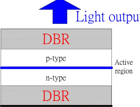
conventional edge-emitting to surface-emitting configuration for light emitting devices are readily established, witnessed by a growing presence of VCSELs components in both tele- and data-communication technologies [17]. Some additional advantages of VCSELs with respect to edge-emitting lasers (EELs) are listed in Table 1-1. However, even in the absence of stimulated emission, resonant-cavity light emitting diodes (RC-LEDs) can also be very useful through enhanced spontaneous emission, low divergence output beams, high spectral purity, good temperature stability, and higher modulation bandwidth [18]. Both devices are characterized by the need for an optical resonator which has high quality or Q-factor and is formed with planar mirrors parallel to the growth surface of the semiconductor heterostructures. The extension of these device concepts to the blue and near-ultraviolet presents significant challenges and opportunities to III-nitrides technology. The nitride-based microcavity structure is composed of a nitride-based cavity space major included an active layer and which is sandwiched by two distributed Bragg reflectors (DBRs). The schematic structure is shown in Figure 1-2. There are three types of resonator to form nitride-based microcavity and shown in Figure 1-3, they are (1) All-epitaxial DBR resonator, (2) All-dielectric DBR resonator, and (3) Hybrid DBR resonator [19]. An acknowledged basic difficulty in applying in situ epitaxial growth techniques to form nitride-based distributed Bragg reflectors for high-Q vertical cavities is the small index of refraction contrast that is achievable within the full AlGaN alloy
range. The samll contrast in the index of refraction between GaN (n~2.35) and A1N (n~2.10) mandates a large number of layer pairs and high aluminum fraction in a multi-layer A1GaN distributed Bragg reflector (DBR) stack, in order to achieve sufficiently high reflectivity (R~0.99) [20]. Furthermore, the high-reflectance region is small with a wavelength band width 10-20 nm. However, a large mismatch in the lattice constant (2.4%) implies difficulties in strain management and potential occurrence of structural defects due to strain relief which can seriously compromise the optical integrity of a high-Q microcavity. To circumvent the problems with as-grown A1GaN DBRs, laser lift-off methods have been used to separate the InGaN multi quantum well (MQW) heterostructure from its sapphire substrate in order to encase it within a high-Q cavity with two dielectric DBRs [21, 22]. In this way, quasi-continuous-wave optically pumped vertical-cavity lasing [21] and resonant-cavity LED operation [22] have been achieved in the 405-415 nm range, at excitation levels comparable to the equivalent current injection in a good edge-emitting diode laser. However, the obvious obstacle to fabricate all-dielectric DBR resonator is posed by the need to separate the nitride-based cavity space from the sapphire substrate. Therefore, the hybrid DBR resonator composed of one in situ grown AlGaN DBR and one dielectric DBR is hopefulness to form high quality nitride-based microcavity [23].
1.4 Quantum Dots Structures
During the last decade, the impressive progress in the epitaxial crystal growth techniques, such as molecular beam epitaxy (MBE) and metal organic chemical vapor deposition leads that the fabrication of low-dimensional semiconductor structures is possible [24]. The effective dimension of semiconductor structure can be reduced from three dimensional bulk materials, to quasi-two dimensional quantum well systems, to quasi-one dimensional quantum wires, and even to quasi-zero dimensional quantum dots. These quantum confined structures with quantum confined effect can modify the electronic and optical properties [25]. For example, the radiative recombination lifetimes in low-dimensional III-V semiconductor structures can be improved. This is due to two factors: the forced increase in overlap of the wavefunctions for electrons and holes, and the changes in the shapes of the density of states distribution for the conduction and valence bands. This leads to higher recombination rates and a narrowing of the gain spectrum. This feature makes quantum confined semiconductor very promising for possible device applications such as an increase in quantum efficiency for LEDs and a decrease in threshold current density for lasers [26].
The quantum confined nano-structures and quantum dot (QD) structures are low-dimensional confinement structures and have many unique physical characteristics. For example, the application of QD structure in LDs has known to have lower threshold
currents due to the enhancement of excitonic effects in the quantum dots [27]. Recently, the fabrication and studies of GaN-based nano-structures have attracted a great deal of interests for potential applications in electronic and optoelectronic devices. It has been reported that the compositional inhomogeneous occurred in InGaN films could form localized In-rich regions in InGaN active layers that play a key role in increasing the efficiency and performance of optoelectronic devices [28]. It was believed that such indium-rich nanoscale structures form the localized states, similar to those of quantum dots, and the localized states can trap significant amount of carriers for radiative recombination, leading to highly efficient light emission [29]. For GaN-based materials, the report suggested that III-nitride QD structures can reduce the effect of defect density on the device performance [30].
Furthermore, QDs structures also play an important role in microcavity devices, because the drawback of such devices is that they suffer from edge effects due to carrier loss and nonradiative recombination which may limit their efficiency. Using QDs as active light sources offer many advantage to overcome such limitation, due to their zero dimensional properties [31]. Therefore, semiconductor QD structure is also a candidate for single photon emitter. QD offers several advantages as a source for single photon. The quantum efficiency and oscillator strength of the dots are very high. The dots do not suffer from photobleaching or shelving, and are stable indefinitely [32]. Unlike
mesoscopic quantum wells, quantum dots allow the number of confined carriers to be controlled without resorting to the Coulomb blockade effect, allowing for higher-temperature operation. The materials used to make the dots are compatible with mature semiconductor technologies, allowing for the sources to be further developed and to be incorporated into larger structures. QDs structures Combine with microcavity structure to couple a single quantum dot to a single mode of a microcavity results in an efficient source of single photons [33].
1.5 Overview of this thesis
This study has focused on the fabrication of optical and electric quantum confined structure grown by metal organic chemical vapor deposition (MOCVD).
Since all the epitaxial structures in this study were grown by MOCVD system, chapter 2 reviews the fundamentals of MOCVD system which includes reaction equations, gas blending systems, reaction chamber, heating system, and in-situ reflectance monitoring. Chapter 3 reports the growth of nitride-based DBR structure used in short wavelength range. The optimized ambient gas during the growth AlN/GaN DBR structure in MOCVD system has been determined by investigating performance of DBR reflectance spectrum, and the serious problem of crack generation in AlN/GaN DBR structure was also been solved by growing an asymmetric DBR structure. After the fabrication of the high quality AlN/GaN DBR structure, an optical quantum confined
structure with a semiconductor microcavity structure has been studied. Chapter 4 reports the characteristic of nitride-based microcavity structure which is composed of a nitride-based cavity space major included an active layer and which is sandwiched by one AlN/GaN DBR structure and one dielectric oxide DBR structure. The characteristic of nitride-based microcavity structure for optical pumping and the electrically driven device has been fabricated and the characteristics will be discussed. The electric quantum confined structure with a quantum dots structure has also been grown and the characteristic were also been studied. Chapter 5 reports the self-assembled InGaN QDs structure grown by MOCVD system. In this chapter, the effect of growth interruption on self-assembled InGaN QDs will be discussed. Chapter 6 is the summary of this thesis.
References
[1] B. Monemar, and G. Pozina, Progress in Quantum Electronics, 24, 239, 2000 [2] Y. Arakawa, IEEE Journal of Selected Topic in Quantum Electronics, 8, 823, 2002 [3] H. Morkoc, Nitride Semiconductors and Devices (Springer Verlag, Heidelberg), 1999 [4] S. N. Mohammad, and H. MorKoc, Progress in Quantum Electronics, 20, 361, 1996 [5] F. Bernardini, V. Fiorentini, and D. Vanderbilt, PHYSICAL REVIEW B, 56, 56, 1997 [6] S. Nakamura and G. Fasol, The Blue Laser Diode. (Berlin, Germany Springer-Verlag)
1997.
[7] I. Akasaki and H. Amano, Jpn. J. Appl. Phys., 36, 5393, 1997.
[8] S. Nakamura, M. Senoh, S. Nagahama, N. Iwasa, T. Yamada, T. Matsushita, H. Kiyoku, and Y. Sugimoto, Jpn. J. Appl. Phys., 35, L74, 1996.
[9] I. Akasaki, S. Sota, H. Sakai, T. Tanaka, M. Koike, and H. Amano, Electron. Lett., 32, 105, 1996.
[10] S. Nakamura, M. Senoh, S. Nagahama, T. Matsushita, H. Kiyoku, Y. Sugimoto, T. Kozaki, H. Umemoto, M. Sano, and T. Mukai, Jpn. J. Appl. Phys., 38, 226, 1999
[11] Pierre Gibart, Rep. Prog. Phys., 67, 667, 2004
[12] Shuji Nakamura,a) Masayuki Senoh, Shin-ichi Nagahama, Naruhito Iwasa, Takao Yamada, Toshio Matsushita, Hiroyuki Kiyoku, Yasunobu Sugimoto, Tokuya Kozaki, Hitoshi Umemoto, Masahiko Sano, and Kazuyuki Chocho, Appl. Phys. Lett., 72, 2014, 1998
[13] J. I. Pankove, M. Leksono, S.S. Chang, C. Walker, B. Van Zeghbroeck, MRS Internet Journal of Nitride Semiconducting Research 1, 161, 1996
[14] S. T. Sheppard, K. Doverspike, W. L. Pribble, S. T. Allen, J. W. Palmour, L. T. Kehias, J. T. Jenkins, IEEE Electronic Device Letters, 20, 610, 1999
[16] P. Mackowiak, and W. Nakwask, J. Phys. D: Appl. Phys. 33, 642, 2000
[17] Kent D. Choquette, and Hong Q. Hou, Procedding of the IEEE, 85, 1730, 1997
[18] Danae Delbeke, Ronny Bockstaele, Peter Bienstman, Roel Baets, and Henri Benisty, IEEE Journal of Selected Topic in Quantum Electronics, 8, 189, 2002
[19] Arto Nurmikko, and Jung Han, MRS Bulletin, 502, 2002 (Conference) [20] T. Someyaa) and Y. Arakawa, Appl. Phys. Lett., 73, 3653, 1998
[21] Y.-K. Song, H. Zhou, M. Diagne, I. Ozden, A. Vertikov, A. V. Nurmikko, C. Carter-Coman, R. S. Kern, F. A. Kish, and M. R. Krames, Appl. Phys. Lett. 74, 3441, 1999.
[22] Y.-K. Song, H. Zhou, M. Diagne, A. V. Nurmikko R. P. Schneider, Jr. C. P. Kuo, M. R. Krames, R. S. Kern, C. Carter-Coman, and F. A. Kish, Appl. Phys. Lett. 76, 1662, 2000 [23] M. Diagne, Y. He, H. Zhou, E. Makarona, A. V. Nurmikko, J. Han, K. E. Waldrip, J. J.
Figiel, T. Takeuchi, and M. Krames, Appl. Phys. Lett., 79, 3720, 2001 [24] Y. Arakawa, phys. stat. sol. (a) 188, 37, 2001
[25] Thierry Taliercio, Pierre Lefebvre1, Mathieu Gallart and Aur´elien Morel, JOURNAL OF PHYSICS: CONDENSED MATTER, 13, 7027, 2001
[26] M. Rowe, M. Vehse, P. Michler, J. Gutowski, S. Heppel, and A. Hangleiter, phys. stat. sol. (c) 0, 1860, 2003
[27] Y. Arakawa and H. Sakaki, Appl. Phys. Lett. 40, 939, 1982
[28] D. Gerthsen*, E. Hahn, B. Neubauer, V. Potin, A. Rosenauer, and M. Schowalter phys. stat. sol (c) 0, 1668, 2003
[29] Richard J. Warburton, Contemporary Physics, 43, 351, 2002
[30] Y. Arakawa, T. Someya, and K. Tachibana, phys. stat. sol. (b) 244, 1, 2001 [31] Li Jiawei, Ye Zhizhen, Nasser NM. Physica A. 16 (2003)244.
[32] V. Zwiller, T. Aichele, and O. Benson, PHYSICAL REVIEW B 69, 165307, 2004
Figure 1-1
Energy band diagram for an ideal abrupt heterojunction of type I
between two different semiconductor materials labeled A and B.
A
E
g
E
g
B
E
c
E
c
E
v
E
v
A
E
g
E
g
B
E
c
E
c
E
v
E
v
Feature EEL VCSEL
Spectral bandwidth Very narrow Narrow
Size of active area Typically 0.5-1×2-10 µm Variable, 5-50 µm in diameter Beam geometry Strong elliptic Circular
Beam divergence High, up to 60°×20° Low, 5°
Number of modes Typically 1 or few 1 or even up to many 10s Coupling to fiber Difficult and sensitive Easy
Coupling efficiency Moderate High Threshold current Approximately 10 mA Some mA Direct modulation
bandwidth
High, up to 10 Gbit/s High, up to 10 Gbit/s
Temperature drift of Pop Fairly high Tendentially low
Environmental sensitivity
Extremely high Moderate
Processing of chip Very specific Similar to LED Final processing Single bar On wafer Burn-in and functional
test
Single on heatsink On wafer
Figure 1-2
The schematic diagram of nitride-based microcavity structure.DBR
DBR
Light output
p-type
n-type
Active
region
Figure 1-3 Three nitride-based microcavity structures: The all-epitaxial mirrors resonator
structure, one amorphous-dielectric mirrors resonator structure, and all-dielectric mirrors resonator structure.
Chapter 2
Metalorganic Chemical Vapor Deposition System
For the past twenty years, metal organic chemical vapor deposition (MOCVD) system has become a commonly used technology for production of III-V compound semiconductor optoelectronic and electronic devices. The term “MOCVD” was originated by Manasevit [1-3], and it was used to express a form of chemical vapor deposition (CVD) utilizing the new process transported metals using organic compounds for one or more of the precursors. Alternative names included OM (OrganoMetallic) CVD, MOVPE (Vapor Phase Epitaxy), and OMVPE are all the same meaning, except epitaxy is a special case of thin film deposition where the layer replicates the crystal structure of the substrate. Because of the improvement in the material quality produced by MOCVD, many important III-V devices have become commercially viable. Indeed, the achievement of growing ultra-bright blue light emitting diodes by MOCVD [4] makes this technology be a leading candidate for manufacturing optoelectronics devices. In this dissertation, we use MOCVD system to grow all the epitaxial structures. The detailed descriptions and specific functions of MOCVD system are given in this chapter.
2.1 Reaction Equations
The MOCVD process for the growth of compound semiconductor materials and devices originated in the pioneering work has been done by H. M. Manasevit. Briefly, MOCVD process relies on vapor transport of the group III alkyls combined with group V hydrides into heated substrate. At the heated substrate, the molecules pyrolyze to produce the group III and group V elements needed for formation of desired III-V semiconductors and subsequent reaction. The simplest case in MOCVD [5] involves a pyrolysis reaction of the vapor of a volatile organometallic compound and a gaseous hydride, given by:
nRH AD
DH A
Rn + n ⎯⎯→ + (2-1)
A and D are the constituent species for the deposited solid. R is an organic radical of some unspecified form, and many organometallic compounds have been studied as sources for the MOCVD processes. Table 2-1 [6] shows some of the more widely used MOs and their key properties. However, the lower order organic radicals are generally used, such as a methyl- or ethyl-radical, and the most important are trimethylgallium (TMGa), triethylgallium (TEGa), trimethylaluminum (TMAl), and trimethylindium (TMIn). Desirable properties include a reasonable vapor pressure at room temperature or below, high purity, low cost, a low affinity for oxygen and water vapor, and low toxicity. Unfortunately, many of the MOs that meet the vapor pressure and purity needs best are also highly reactive with oxygen. They are therefore contained in stainless steel bubblers,
and great effort is made to avoid their contamination by air. Contrasting with V sources, metalorganic group III source are either liquids, such as TMGa, TEGa, and TMAl, or solids such as TMIn. Therefore, the organmetallic constituents generally are transported to a heated substrate by passing a carrier gas, over or through the compound contained in a constant-temperature bubble vessel. Highly purified hydrogen or nitrogen is bubbled through the liquid to transport the material into the reactor. A knowledge of the vapor pressure (at the bubble temperature and pressure) and the carrier gas flow rate is sufficient to determine the transport rate.
On the other hand, most MOCVD growth of III-V compound semiconductors and alloys involves the use of hydrides, such as arsine, phosphine, or ammonia for the column V species. In principle, these are the simplest of column V sources to use because they are already gaseous and supplied from simple cylinder-based delivery system. In spite of the fact that they are extremely toxic, since they are relatively inexpensive with high purity layers.
The dopants processes are available in the form of MOs in bubblers (for example, Cp2Mg), or in the form of gases (for example, SiH4). Because of the concentration may
be varied over a wide range, the dopant sources have to adjust the concentration, typically with a dilution network.
vapors from the different alloy constituents in the appropriate vapor phase ratio to form the desired composition. A general equation for a ternary alloy is given by:
(2-2) For GaN-based material growth, the first MOCVD system design for GaN growth was developed by Maruska and Tietjen [7]. Soon after, Manasevit applied this technique to grow GaN onto sapphire substrate [8]. The choice of sapphire substrate results from the facts that no GaN bulk substrate are available and a very stable material is required to deal with the high temperature required for GaN growth at around 1000oC.
Based on the equation (2-1), the GaN epitaxy process by using MOCVD can be written:
(2-3) which v is vapor and s is solid. This simple equation, however, ignores the complicated reaction path and reactive species in the reactor. The incoming materials partially decompose and are then adsorbed on the surface. Then, they decompose further or are desorbed. The atoms and radicals move around on the surface with growth occurring at steps for smooth, two-dimensional layers, replicating the structure of the substrate [9]. In fact, the detail of the reaction is still unknown. Nishizawa, Abe and Kurabayashi (1985); Denbaars et al. (1996) [10] reported a reaction pathway arise form growing GaAs epitaxial layers involves homogenerous decomposition of TMGa :
nRH D B A DH B R x A xRn +(1− ) n + n ⎯⎯→ x 1−x + ) ( 3 ) ( ) ( ) ( ) (CH3 3Ga v +NH3 v ⎯⎯→GaN s + CH4 v
(2-4) (2-5) (2-6) In the other hand, the group V source, NH3, is considered to decompose heterogeneously
on the GaN surface or reactor wall to provide atomic nitrogen, or a nitrogen containing radical at high grow temperature.
(2-7) Combine the above mentioned equation, one possible growth mechanism of GaN that occur at the solid/vapor interface could be expressed as follows:
(2-8) Although the growth mechanism of GaN can be briefly expressed by Eq. (2-8). The
most difficult topic is the kinetics of the process and growth mechanism occurring at solid/vapor interface during MOCVD growth.
Optimization of MOCVD grown condition is typically done by empirical studies of external parameters such as grown temperature, V/III ratio, and mass flow rate. These studies have identified three regions of growth: mass transport limited, desorption and surface kinetically limited regimes. Conventional GaN MOCVD growth is usually performed in mass transport limited regime that takes place over a wide temperature (600~1100oC), and the growth is limited by mass transport of the column III reactant to
) ( ) ( ) ( ) ( ) (CH3 3 v Ga CH3 2 v CH3 v Ga ⎯⎯→ + ) ( ) ( ) ( ) ( ) (CH3 2 v Ga CH3 v CH3 v Ga ⎯⎯→ + ) / ( ) / ( ) / ( (3 ) 3 s v NH s v xH s v NH ⎯⎯→ −x + ) ( ) ( 2 / 1 ) ( ) / ( ) / ( ) (CH3 s v NH s v GaN s H2 v CH3 v Ga + ⎯⎯→ + + ) ( ) ( ) ( ) (CH3 v Ga v CH3 v Ga ⎯⎯→ +
the growing interface.
2.2 Gas Blending Systems
The MOCVD system used in this dissertation is EMCORE D75 system and the system of EMCORE D-75 is illustrated in Figure 2-1. There are four major components in the modern MOCVD system as shown in Figure 2-2: (1) the gas blending system including the source alkyls and hydrides and all of the valves, plumbing, and instruments necessary to control the gas flows and mixtures; (2) the reactor chamber in which the pyrolysis reaction and deposition occurs; (3) the heating system used to obtain pyrolysis temperature; and (4) the vacuum and scrubbing system. All of them are controlled by a programming logical unit. The gas blending unit is responsible for transporting and mixing the precursors. The reactor chamber with a heated susceptor determines the crystal quality, the layer thickness, and the uniformity. The vacuum and scrubbing system is responsible for exhausting the gas after reaction and balancing the pressure in reactor chamber. The scrubbing system deals with the toxic gas after reaction for the safety considerations. Figure 2-3 describes the basic function of these components.
The gas blending system is illustrated in Figure 2-4. The gas blending system [11-15] for D-75 MOCVD system is a very clean, leak-free network of stainless- steel tubing, automatic valves, and electronic mass flow controllers. Hydride delivering modules
generally require a few valves and an electronic mass flow controller, since these sources are already provided as dilute, high pressure gases in gas cylinders. Alkyl delivery modules are more complicated. These high-vapor-pressure sources are contained in stainless-steel bubblers and held in a temperature-controlled bath to maintain a stable vapor pressure over the liquid or solid sources. An important part of the gas blending system is the supply of carrier gases within a vent-run configuration, show in Figure 2-4 as the injection block. The design of the injection block can avoid transients from switching or dead space. The vent-run valves couple the individual source modules to the supply line. The stable and controllable source flow rate can then be established and stabilized while the valve is vented to a waste line and prior to injection into the run supply line as shown in Figure 2-4. The absolute and differential pressures are all dynamically controlled, so that when switching of flows occurs there are no pressure transients which could upset the transition from one layer to the next. This is particularly important for quantum well based devices, which often require monoatomically abrupt interface. A main carrier gas flow is also directed to the reactor, which combination of all flows preferably taking place in the reactor.
2.3 Reactor Chamber
into a heated zone where an appropriate substrate is located, and the basic pyrolysis reactions take place. The most common reaction chambers are the vertical and horizontal chamber shown in Figure 2-5 [16]. The horizontal is easy to construct provide a good glass blower and the gases flow parallel to the wafer, from one side to the other. Reactant depletion effects result in a decreasing growth rate across the wafer, which can be mitigated by tilting the wafer, increasing the carrier gas flow, and rotating the wafer. A lateral depletion effect becomes important for wider tubes, making scale-up of this geometry difficult. In the vertical geometry, the gases flow perpendicular to the wafer surface. It is more complex mechanically than the horizontal, since it is desirable to rotate the wafer to average out uneven heating effects. It is also difficult to scale up, because of worsening uniformity and is subject to convective recirculation. However, these issues can be overcome by rotating the substrate rapidly. The disk rotation pulls the incoming gases to the wafer surface, and providing the reactants are fed in uniformly across the inlet result in a uniform deposit over the entire surface. The schematic image is shown in Figure 2-6 [17].
The reactor of geometry of EMCORE D-75 system is shown in Figure 2-7, which is a vertical type chamber and made up with a double walled water-cooled stainless-steel chamber. The alkyl and hydride sources inject into the reactor via regulated mass flow controllers which are fully computer controlled. The flow rate ratio between mass flow
controllers labeled 1 to 3 for alkyls injection determines the growth rate and the uniformity of the epitaxial layer. Alkyl and hydride sources do not mix together until they reach the wafer surface in order to prevent the pre-reaction. The wafer carrier for D-75 type MOCVD contains a two-inch wafer recesses and is driven by the susceptor which was on top of a spindle rotation. The spindle rotation is by means of a high speed motor driving a toothed belt. To achieve uniformly laminar gas flow near the wafer surface at relatively low pressure, the rotation speed is 900 rounds per minute. The reactor pressure for the epitaxial growth is maintained by a throttle valve.
2.4 Heating System
The susceptor may be heated in any manner that avoids directly heating the neighboring surface, especially upstream of the sources. There have been several methods which are included RF introduction, infrared heating, and resistance heater, used in MOCVD system to heat the wafer susceptor [18-21]. In EMCORE D-75 system, the filament which is a type of resistance heater is used as heater and the image of filament is shown in Figure 2-8. The growth temperature is controlled by a temperature controller, which is better than ± 1oC with a PID controlled ac low voltage power supply.
2.5 In-Situ Reflectance Monitoring During III-Nitrides Growth
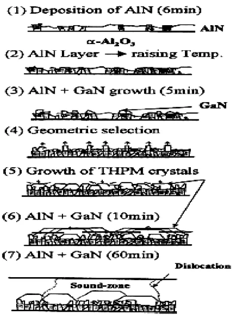
For many years, high vacuum growth techniques such as MBE have enjoyed the advantage of using in situ diagnostic tools such as RHEED to determine substrate surface conditions and measure growth rates. Now MOCVD has responded with a variety of optical techniques to perform diagnostic on the layers as they grow [22]. Indeed, the in-situ monitoring of optical techniques is very useful for growing optoelectronic devices such as VCSELs due to the stringent requirement of phase matching. The in-situ monitoring is also an important tool to grow III-Nitride materials on foreign substrate, such as sapphire, because the limitation of homoepitaxial substrate absence is usually overcome by growing a low-temperature (LT) AlN [23] or GaN [24] nucleation layer on a sapphire substrate before the high-temperature (HT) growth. A growth mode of GaN film on sapphire substrate covered with a thin AlN buffer layer is shown in Figure 2-9. In order to realize the growth information during growing GaN, the in-situ monitoring tool is usually used to extracting growth information.
In our D-75 system, we use an in-situ normal incidence reflectance method to extract the information of growth rate and crystal quality. The tungsten-lamp reflectometry is applied as the in-situ monitoring in D-75 type MOCVD system. The schematic of the configuration is shown in Figure 2-10. Two optical heads are mounted on the top flow flange of the reactor and monitoring the growth conditions for the upper and lower points
of the wafer surface. An optical head couples two fibers; one is from the light source with the continue band wavelength, and the other is to the detector. Suppose the optic index of thin film materials is different from the substrate, the reflectance and interference from the underlying interface can be described as R= r2, and r can be described as [25]
(2-9) where β2 =4πnd/λ is the phase shift in the film, r∞ and r are the reflectance of an i
infinitely thick film of the top layer and the internal layer reflectance, respectively. Theexp(−i4πβ2) term describe and oscillatory behavior of β2. Thus growth rate can be determined with the refractive index at certain growth temperature at a given wavelength. The growth rate can be obtained by
(2-10) where λ is the chosen wavelength, Td is the oscillation period of the reflectivity curve,
nλ is the refractive index of the epitaxial layer at the growth temperature for λ. This is
very useful controlling the thickness of the LT nucleation layer. Figure 2-11 shows the example for the measured reflectivity of a GaN bulk structure.
Furthermore, applying the in-situ monitoring system, we can also do temperature calibrations. In the former case, one can perform temperature calibration with eutectic wafers (Al-coated Si wafers or Silver-coated Si wafers) quickly and easily by plotting the reflectance as a function of temperature, while the temperature of the reactor is ramped
) 4 exp( 1 ) 4 exp( ) ( 2 2 πβ πβ − + − + = ∞ ∞ i i r r i r r t r λ
λ
T
n
G
R=
d/
2
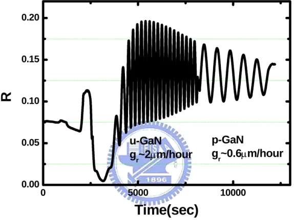
slowly. As the temperature ramping up to the melting point of aluminum or silver, 660oC, and 961oC, respectively, the reflectance would be drop down rapidly. Thus one could know the meter temperature is the metal melting point. In the latter case, one can design a “calibration” structure that contains layers of different compositions or different growth condition in a single growth run without requiring any post growth characterization. Figure 2-12 shows the typical reflectance plot as a function of time depicting the growth of different layers for calibration of growth rate. The result shows that the growth rates of layers can be clearly judged.
The in-situ monitoring system is PC-based and integrates measurement and analysis software with spectrophotometer and fiber optic measurement hardware. Figure 2-13 shows the schematic diagram of the in-situ monitoring apparatus. Light source is a tungsten-halogen bulb that supplied light form approximately 400nm to 3000nm. This light is delivered to and collected from the sample through a fiber optic cable bundle and a lens. The intensity of the reflected light is measured at 512 different wavelengths with a spectrometer. The spectrometer uses a diffraction grating to disperse the light and a linear photodiode array to measure the light at the different wavelength. The photodiode array operates by integrating the current generated by light falling on each of the 512 pixels. After a user-selectable integration time, the accumulated charge in each photodiode is read by the computer. Appropriate adjust the integration time to meet the proper signal
References
[1] J. B. Mullin, S. J. C. Irvine, and J. Tunnicliffe, J. Cryst. Growth, 68, 214, 1984 [2] B. Cockayne, and P. J. Wright, J. Cryst. Growth, 68, 223, 1984
[3] H. M. Manasevit, Appl. Phys. Lett. 12, 156, 1968
[4] S. Nakamura, T. Muksi, and M. Senoh, Appl. Phys. Lett. 64, 1687, 1994 [5] H. M. Manasevit, and W. I. Simpson, J. Electrochem. Soc, 116, 1725, 1969 [6] Alan G. Thompson, Materials Letters, 30, 255, 1997
[7] H. P. Maruska, and J. J. Tietjen, Appl. Phys. Lett., 15, 367, 1969.
[8] H. M. Manasevit, F. Erdmann and W. Simpson, J. Electrochem. Soc, 118, 1864, 1971 [9] S.Yu. Karpov, V.G. Prokofjev, E.V. Yakovlev, R.A. Talalaev, Yu.N. Makarov, MRS J.
Nitride Semicond. Res. 4, 4, 1999
[10] S. P. DenBaar, B. Y. Maa, P. D. Dapkus, and H. C. Lee, J. Cryst. Growth, 77, 188, 1986 [11] H. Kawai, I. Hase, K. Kaneko, and N. Watanabe, J. Cryst. Growth, 68, 406, 1984 [12] C. C. Wang and S. H. McFarlane, III, J. Cryst. Growth, 13/14, 262, 1972
[13] E. J. Thrush, J. E. A. Whiteaay, and Wale-Evans, J. Cryst. Growth, 68, 412, 1984 [14] R. D. Dupuis, L. A. Moudy, and P. D. Dapkus, Inst. Phys. Conf, Ser., 45, 1, 1978 [15]J. S. Roberts, and N. J. Mason, J. Cryst. Growth, 68, 422, 1984
[16] M. J. Ludowise, J. Appl. Phys., 58, R31, 1985 [17] S. Yu. Karpov, J. Cryst. Growth, 248, 1, 2003
[18] H. Beneking, A. Escobosa, and H. Kraeutle, J. Electron. Mater., 10, 473, 1981. [19] C.C. Hsu, R. M. Cohen, and G. B. Stringfellow, J. Cryst. Growth, 63, 8, 1983 [20] J. P. Noda and A. J. SpringThorpe, J. Electron. Mater., 9, 601, 1980.
[21] R. H. Moss and P. C. Spurdens, J. Cryst. Growth, 68, 96, 1984 [22] D. E. Aspnes, IEEE J. Select. Topic Quant Elect., 1, 1054, 1995
[24] S. Nakamura, Jpn. J. Appl. Phys., 30, L1705, 1991
Table 2-1 The names and properties of some of a the more commonly used
metalorganic (MO) compounds for III-V and II-VI MOCVD ”common” implies
a widely used material.
Element Name Symbol
Vapor pressure
(Torr at oC)
Liquid
or Solid Comments
Aluminum Trimethylaluminum TMAl 9 at 20 L Common
Antimony Trimethylantimony TMSb 50 at 10 L Arsenic Tertiarybutylarisine Trimethylarsenic TBAs TMAs 125 at 20 300 at 25 L L high C Cadmium Diethylcadmium Dimethylcadmium DECd DMCd 1at 30 28 at 20 L L Gallium Triethylgallium Triisopropylgallium Trimethylgallium TEGa TIPGa TMGa 3 at 20 1 at 25 65 at 0 L L L Common Common Indium Ethyldimethylindium Trimethylindium EDMIn TMIn 2 at 20 2 at 20 L S Common
Iron iron Biscyclodipentadienyl Cp2Fe 1 at 20 S Doping InP
Magnesium
Biscyclodipentadienyl-magnesium Cp2Mg 0.1 at 35 S Sp-dopant
Phosphorus Tertiarybutylphosphine TBP 250 at 20 L
Tellurium Diethyltelluride DETe 7 at 20 L
Zinc Diethylzinc Dimethylzinc DEZn DMZn 12 at 20 120 at 0 L L
Figur
e 2-1
Figure 2-4 Schema of gas blending system in MOCVD.
Pressure balancin g unit Pressure balancin g unit To reactor Hydride inject To reactor Alkyl inject To scrubber NH3 SiH4 Purified H2 TMGa TMAl TMIn Pressure controller Automatic valve Mass flow controller Injection block RUN RUN VENTFigure 2-5 Two types MOCVD systems (a) Vertical chamber,
200 RPM 400 RPM
800 RPM 1600 RPM
3 2 1
Alkyl inject Hydride inject
Double o-ring
Water-cooled flow flange
screen
Wafer Wafer carrier
Reactor wall Exhaust Spindle filament Susceptor Inner thermal couple Water-cooled baseplate
Figure 2-9 Model for the growth of GaN grown by MOCVD using the
Figure 2-10 Schematic of in-situ monitoring configuration. By collecting the
reflection of a Xe-Lamp light perpendicularly impinging on the wafer surface
Xe-Lamp Detector fiber
Wafer
Reactor
Figure 2-11 The measured reflectivity of GaN bulk layer on sapphire.
0
1000 2000 3000 4000 5000 6000 7000 8000
0.00
0.05
0.10
0.15
0.20
0.25
v
vi
iii
ii
i
R
e
fle
c
ta
n
c
e
Time (s)
Figure 2-12 The calibration of growth rate for different nitride-based materials
by in-situ reflectance measurement.
0 5000 10000 0.00 0.05 0.10 0.15 0.20
p-GaN
g
r~0.6
µm/hour
u-GaN
g
r~2
µm/hour
R
Time(sec)
Figure 2-13 The schematic diagram of the controlling apparatus for in-situ
Chapter 3
Fabrication of the Nitride-Based Distributed Bragg Reflector
Chapter 3 reports the fabrication of high reflectance nitride-based distributed bragg reflector by MOCVD technique. We start this chapter with the discussion of DBRs characteristics. Following the DBR discussion, the monolithically grown issues of nitride-based DBR structure will be described. After that, the optimized ambient gas during the growth AlN/GaN DBR structure in MOCVD system has been determined by investigating performance of DBR reflectance spectrum. Finally, a technique of suppressing crack generation in AlN/GaN DBR structure with non-quarterwave stacks DBR structure will be reported.
3-1 Characteristics of Distributed Bragg Reflectors
We start this section with the transfer matrix method in stacks of thin films. We construct a computational simulation program for the transfer matrix. Then, based on the simulation, we’ll discuss the DBR reflectance spectrum with different pairs, different index contrasts, and different ratios of thicknesses for the two composed materials in DBR structures.