國 立 交 通 大 學
電子工程學系 電子研究所碩士班
碩 士 論 文
利用特殊接觸電極研究橫向擴散元件
之自發熱效應與可靠度
Investigation of Self-Heating and Reliability Issues
in Lateral DMOS by Using an Additional Metal
Contact Structure
研 究 生 :林家福
指導教授 :汪大暉 博士
中華民國 九十六 年 六 月
利用特殊接觸電極研究橫向擴散元件之
自發熱效應與可靠度
Investigation of Self-Heating and Reliability Issues in
Lateral DMOS by Using an Additional Metal Contact
Structure
研 究 生 : 林家福 Student : Jia-Fu Lin
指導教授 : 汪大暉 博士 Advisor : Dr. Tahui Wang
國立交通大學
電子工程學系 電子研究所碩士班
碩士論文
A Thesis
Submitted to Department of Electronics Engineering & Institute
of Electronics
College of Electrical and Computer Engineering
National Chiao Tung University
in Partial Fulfillment of the Requirements
for the Degree of
Master
in
Electronic Engineering
June 2007
Hsinchu, Taiwan, Republic of China.
利用特殊接觸電極研究橫向擴散元件之
自發熱效應與可靠度
學生:林家福
指導教授:汪大暉 博士
國立交通大學 電子工程學系 電子研究所
摘要
隨著半導體業的發展,高功率金氧半場效電晶體被廣泛的應用在電力電子元 件上,LDMOS(橫向兩次擴散之金氧半場效電晶體)通常在高壓積體電路中做驅動 元件、電力切換元件、射頻功率電晶體。在本論文中,主要是利用特殊接觸電極 來對 LDMOS 做可靠度分析。 在此論文中,主要討論在不同的熱載子加壓後,LDMOS 的電性退化程度, 我們提出一個三區域的電荷幫浦實驗(three-region charge pumping technique)來觀 察不同的區域有何不同的損害產生。同時利用特殊的金屬電極來研究 LDMOS 的 低頻雜訊(Flicker Noise),可以了解到不同的閘極電壓下所量到的低頻雜訊分別代 表不同的區域,最後利用二維方向的模擬來解釋實驗上的結果。在實驗上發現, 在最大閘極漏電流的加壓條件下,由於在 LDMOS 的通道部分有介面缺陷及在鳥 嘴區有氧化層電荷的產生,所以造成最嚴重的集極電流退化以及低頻雜訊的增 加,同時利用電荷幫浦實驗,可萃取介面缺陷以及氧化層電荷產生的速率。 接著,我們利用特殊的金屬接觸電極以及快速的暫態電路來研究 LDMOS 的 自發熱效應(self-heating effect)。自發熱效應與瞬間熱載子加壓後的元件退化關係 i亦在此論文中研究。研究發現,交流的加壓條件由於 LDMOS 沒有自發熱效應, 所以會比直流的加壓條件有較嚴重的熱載子退化。交流加壓的頻率與退化程度同 時也在此論文中研究。
Investigation of Self-Heating and Reliability
Issues in Lateral DMOS by Using an Additional
Metal Contact Structure
Student: Jia-Fu Lin Advisor: Dr. Tahui Wang
Department of Electronics Engineering &
Institute of Electronics
National Chiao Tung University
Abstract.
Lateral Double-Diffused MOS (LDMOS) have been widely utilized in power electronics, for example, LCD drivers, power switch, and ratio frequency power transistor in high voltage integrated circuits. In this study, we will characterize the self-heating and hot carrier reliability issues in LDMOS by using an additional metal contact structure.
Degradation of electrical characteristics in LDMOS transistors in various hot carrier stress modes is investigated. A novel three-region charge pumping technique is proposed to characterize interface trap (Nit) and bulk oxide charge (Qox) creation in the LDMOS. A special metal contact structure is fabricated to identify the flicker noise in MOS and LDMOS. The correlation of flicker noise degradation and stress induced oxide damage region will be analyzed. A two-dimensional numerical device
simulation is performed to explain the measurement result. Our characterization shows that max. Ig stress causes largest drain current degradation and flicker noise degradation because of both interface trap generation in the channel and bulk oxide charge creation in the bird’s beak region. The growth rates of Nit and Qox are extracted from the proposed charge pumping method.
Self-heating effect (SHE) in LDMOS is also investigated by using the special metal contact structure and a fast transient circuit. Transient hot carrier degradation in LDMOS is also investigated. Our characterization shows that drain current degradation in AC stress is more serious than in DC stress because of the elimination of self-heating effect. The stress-frequency dependence of device degradation mode due to self-heating effect will be analyzed.
Acknowledgement
本篇論文之所以能夠完成,乃是無數人合力研究與幫忙互助的結果。 首先,我要感謝我的指導教授-汪大暉老師,能夠提供一個設備完善的實驗 資源,並細心與耐心的指導,讓我們得以在這浩瀚無涯的學術之海,一窺其神秘 之處。另外,博士班學長-志昌學長、煥淇學長、俊榮學長,也都能在最適當的 時間,給予我幫助與開導,尤其是志昌學長,兩年來的無私的指導,使我在實驗 上能夠很容易就上手,並且學習到新的知識與觀念。已經畢業的 93 級學長姐- 冠潔、強哥和至宸,則是帶領我進入實驗室,和教導我量測技術和實驗原理的大 功臣。 在這兩年的時間裡,因為有同學-小鴨、阿雄、Adorken、馬克吳的陪伴, 使得兩年的研究生活充滿著愉悅的氣氛。以及 95 學弟妹-元鵬、彥君、子華、 佑亮、勖廷、柏凱的陪伴,這些都是不可磨滅的美好回憶。 最後,我要感謝我的父母以及女友依珊,在我漫長的求學期間給予我鼓勵與 支持。讓我能沒有後顧之憂的情況下讀書,並完成碩士學位。 謝謝! 2007.6vi
Contents
Chinese Abstract
i
English Abstract
iii
Acknowledgements v
Contents vi
Figure & Table Captions
vii
Chapter 1 Introduction
1
Chapter 2 Drain Current Flicker Noise Degradation in
Various Hot Carrier Degradation Modes 5
2.1 Introduction
5
2.2 Three-Region Charge Pumping Technique
6
2.3 Flicker Noise Measurement
6
2.4 Three Hot Carrier Stress Modes
7
2.4.1 Max. I
bStress Mode
72.4.2 Vg~1/2Vd Stress Mode
82.4.3 Max. I
gStress Mode
82.5 Summary
9
Chapter 3 Impact of Self-Heating Effect on Hot Carrier
Degradation 28
3.1 Introduction
28
3.2 Self-Heating Effect
28
3.3 AC Hot Carrier Stress
30
3.4 Degradation Characteristics in AC/DC Stress
30
Chapter 4 Conclusions
46
Reference 47
Figure & Table Captions
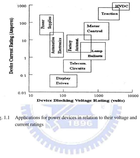
Fig. 1.1 Applications for power devices in relation to their voltage and current ratings
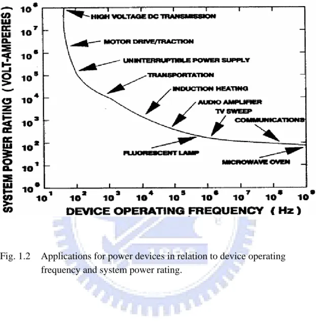
Fig. 1.2 Applications for power devices in relation to device operating frequency and system power rating.
Fig. 2.1 (a) Cross-section of a metal contact n-LDMOS and corresponding flat-band (solid line) and threshold (dash line) voltage distribution. The device is divided into three parts, Lchan (channel region), Lacc (accumulation region), and Lfox (field oxide region).
(b) Illustration of a charge pumping measurement wave form. The Vgh=12V is fixed and Vgl varies from +3.6 to -40V.
Fig 2.2 (a)Substrate current and gate current versus gate voltage in a LDMOS. Three different stress modes are shown in the figure, mode A (maximum Ib), mode B (Vg~1/2Vd), and mode C (maximum Ig).
(b)The bias conditions of the three stress modes.
Fig. 2.3 Typical CP current in a n-LDMOS. The three stages of the CP current correspond to the three regions of the device. The flat-band voltage of each region is indicated in the figure. The frequency in charge pumping measurement is fixed at 200 KHz.
Fig. 2.4 (a) I-V characteristics in MOS and LDMOS at low gate voltage.
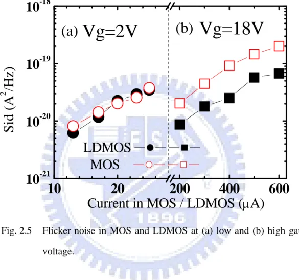
(b) I-V characteristics in MOS and LDMOS at high gate voltage. Fig. 2.5 Flicker noise in MOS and LDMOS at (a) low and (b) high gate
voltage.
stress. Upward shift of the Icp in stage 1 implies the generation of interface trap in the accumulation region.
(b) Two-dimension device simulation of impact ionization (IIG) distribution in stress mode A.
Fig. 2.7 (a) Low gate voltage and (b) High gate voltage flicker noise before and after mode A stress. The enhancement of high gate voltage flicker noise is caused by trap creation in the drift region.
Fig. 2.8 (a) Charge pumping current versus Vgl before and after 1400 sec. mode B stress. The shift of the flat-band voltage in stage 2 implies the generation of negative oxide charge in the accumulation region.
(b) Two-dimension device simulation of impact ionization (IIG) distribution in stress mode B.
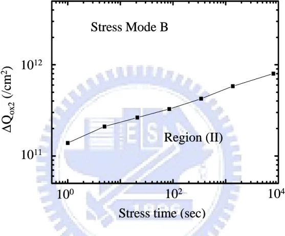
Fig. 2.9 Region (II) oxide trapped charge growth rate in stress mode B.
Fig. 2.10 Linear drain current (Idlin) degradation rate measured at Vg/Vd=40V/0.1V in stress mode B.
Fig. 2.11 (a) Low gate voltage and (b) High gate voltage flicker noise before and after mode B stress. The enhancement of high gate voltage flicker noise is caused by damage in the drift region
Fig. 2.12 (a) Charge pumping current versus Vgl before and after 1000 sec. mode C stress. Upward shift of the Icp in stage 1 indicates interface trap generation in the channel region, and rightward shift of flat-band voltage in stage 2 implies oxide charge creation in the accumulation region.
(b) Two-dimension device simulation of impact ionization (IIG) distribution in stress mode C.
Fig. 2.13 Subthreshold characteristics before and after mode C stress. The swing degradation was attributed to interface trap generation in the channel
region.
Fig. 2.14 Linear drain current versus Vg before and after mode C stress. Fig. 2.15 Region (I) interface trap growth rate in stress mode C.
Fig. 2.16 Region (II) oxide charge growth rate in stress mode C.
Fig. 2.17 Idlin degradation versus stress time in stress mode C. The degradation is mainly caused by negative oxide charge creation in the drift region.
Fig. 2.18 (a) Low gate voltage and (b) High gate voltage flicker noise before and after mode C stress.
Table 2.1 Summary of major oxide and device performance degradations in various stress modes.
Fig. 3.1 Measurement circuit setup for transient drain current and internal voltage (VI) measurement. The resistance (10Ω) is smaller than the total resistance (~40V/10mA~4kΩ).
Fig. 3.2 Comparison of drain current measured by Agilent 4156 (DC measurement) and an oscilloscope (transient measurement) for different device widths and lengths at Vg/Vd=40/40.
Fig. 3.3 (a) Normalized drain current versus drain voltage by DC measurement for two different gate widths (b) Comparison of normalized drain current versus drain voltage by DC and transient measurements. The measurement Vg is 40V.
Fig. 3.4 The cross-section of a LDMOS and flat-band voltage distribution in each region. The metal contact (I) is arranged in the bird’s beak region with a n+ implant. This metal contact is small enough that width it would not affect the electrical characteristics of a LDMOS.
Fig. 3.5 Internal voltage versus gate voltage in a LDMOS. An increase in an internal voltage is observed in the transient measurement.
Fig. 3.6 Simulation of temperature distribution in a LDMOS for (a) Vg=10V and (b) Vg=40V.
Fig. 3.7 Power consumption versus Id degradation.
Fig. 3.8 Substrate current and gate current versus gate voltage in a LDMOS.
Fig. 3.9 Idlin degradations in AC and DC stress conditions in max. Ib and max.
Ig stress modes.
Fig.3.10 (a) Idlin degradation versus stress frequency. A transition frequency is observed around f1=20kHz.
(b)Idlin degradation versus duty cycle.
Fig. 3.11 (a) The transient of an internal voltage (VI) for a gate pulse of 50μs
with Vg/Vd=40V/40V. A decreasing VI is observed after a heating
time around 5μs.
(b) Idlin degradation versus on-state pulse time (=duty
cycle/frequency). The transition frequency (f1) in Fig. 3.10(a) is also indicated in the figure, which corresponds to an on-state pulse time of 5μs.
Fig. 3.12 Idlin degradation rate after max. Ig AC and DC stress. The stress
frequency =20kHz and duty cycle=0.1.
Fig. 3.13 Threes region charge pumping measurement results after maximum Ig AC stress and maximum Ig DC stress. A flat-band voltage shift and an increased ICP are observed in accumulation region and in channel region, respectively.
Fig. 3.14 Two-dimensional device simulation of impact ionization generation (IIG) distribution (a) with heat flow analysis (corresponding to max. Ig DC stress mode) and (b) without heat flow analysis (corresponding to max. Ig AC stress mode). A larger IIG region is
Chapter 1
Introduction
In recent years, power device are strongly demanded for the applications in driver circuits [1], power switches [2], and ratio frequency (RF) power amplifiers [3]. The integrated bipolar, complement metal-oxide-semiconductor (CMOS), and double-diffused metal-oxide-semiconductor (DMOS) process has been developed to realize complex single power ICs [4,5]. Among the candidates of high-voltage devices, lateral DMOS (LDMOS) transistors are most attractive because they can easily integrated with standard low-voltage CMOS process [2,4-5]. Since the LDMOS has been widely utilized in high-voltage and high-current output circuits [6,7], the reliability issues in both DC (Fig. 1.1) and AC ( Fig. 1.2) conditions becomes more and more important.
Hot carrier effect, flicker noise, and self-heating effect are three major reliability issues in LDMOS. In driver application, LDMOS is biased at high drain voltage, which would result in serious hot carrier degradation. Various hot carrier stress modes may generate interface traps and oxide charge in different regions of the device. The profiling of trap distribution and characteristics is important to the study of the device reliability. For RF power amplifiers, the LDMOS is operated in high-power and high-frequency conditions. High-power would increase heat generation in LDMOS and thus the self-heating effect can be observed. In addition, as the LDMOS is used in amplifier application, low frequency noise (flicker noise) behavior would become important. In order to reduce the low frequency noise in LDMOS, the correlation between stress mode and flicker noise degradation must be studied. Since LDMOS is sometimes subjected to AC stress rather than DC stress, we also investigate the effect
of transient hot carrier degradation [10] especially for temperature-related reliability issues.
This thesis is organized as follows: Chapter1 is introduction. Chapter2 shows various DC hot carrier degradation modes and their corresponding flicker noise charcateristics. A three-region charge pumping technique and two-dimensional device simulation are used. Chapter3 shows the impact of self-heating effect on hot carrier degradation in LDMOS. Transient circuit measurement is used to characterize self-heating effect. A special metal contact structure is fabricated to characterize the self-heating time and internal voltage. Finally, we will make a brief conclusion.
Fig. 1.1 Applications for power devices in relation to their voltage and current ratings
Fig. 1.2 Applications for power devices in relation to device operating frequency and system power rating.
Chapter 2
Drain Current Flicker Noise Degradation in
Various Hot Carrier Degradation Modes
2.1 Introduction
Recently, LDMOS has been widely utilized in high-performance radio frequency (RF) components. The signal-to-noise ratio in RF power amplifiers will seriously affect the device performance. In order to reduce low-frequency noise in analog devices, the physical origin of flicker noise in LDMOS devices should be further explored. Since LDMOS is always biased at high drain voltage, hot carrier degradation would become a serious issue. Thus, various hot carrier stress modes
induced oxide damage should be discussed. In this chapter, we used a three-region charge pumping (CP) technique to probe
hot carrier stress induced oxide damage in a LDMOS. The n-LDMOS used in this work was processed in a 0.18μm CMOS technology with a gate oxide thickness of 100nm and a field oxide thickness of 500nm. The operation voltages are Vg=40V and Vd=40V. Fig. 2.1(a) shows the cross-section of a LDMOS with an additional metal contact to sense an internal voltage. This small contact is arranged in a drift region with a n+ implant. The device is divided into three regions. Region (I) is the channel region. Regions (II) and (III) are the accumulation region and the field oxide region. The length of each region is denoted by Lchan(=3μm), Lacc, and Lfox, respectively. The gate width is 20μm and the threshold voltage is 1.5V. The device flat-band voltage (VFB, solid line) and threshold voltage (VT, dash line) distribution of the three regions are plotted in Fig. 2.1(a). A two-dimensional device simulation is performed to
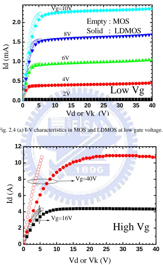
identify an impact ionization generation (IIG) region in the device. In addition, two flicker noise measurements, low Vg (Vg=2V, Vd=0.1V) noise and high Vg (Vg=18V, Vd=0.1V) noise, are performed before and after hot carrier stress.
Three stress modes, mode A (max. Ib), mode B (Vg~1/2Vd), and mode C (max. Ig) are investigated. The Ig-Vg and Ib-Vg of a n-LDMOS are shown in Fig. 2.2(a). The maximum Ib (mode A) occurs in Vg/Vd=8V/50V and maximum Ig (mode C) occurs in Vg/Vd=50V/50V. The bias conditions of the three stress modes are also shown in the Fig. 2.2(b). Subthreshold slope and linear drain current (Idlin) are measured to monitor device performance degradation.
2.2 Three-Region Charge Pumping Technique
The gate voltage waveform in CP measurement is illustrated in Fig. 2.1(b) with a fixed Vgh=12V and a variable Vgl. For the 100nm thick gate oxide, Vgl is switched from +3.6V to -40V without a significant gate oxide tunneling current. In this Vgl range, all the three regions of the device can be probed. The measurement frequency is 200 kHz. Typical CP measurement result is shown in Fig. 2.3. The charge pumping current (Icp) exhibits three stages, corresponding to the three regions of a n-LDMOS respectively. It should be noticed that each stage has their corresponding threshold and flat-band voltage. By measuring the change of Icp and VFB after stress in each stage, we are able to separate Nit and Qox in each region of the device, for example, ΔNit(channel)=ΔIcp(stage 1)/qfWLchan, ΔQox(acc.)=ΔVFB (stage 2)·C/q and so on.
2.3 Flicker Noise Measurement
A special device structure incorporating a metal contact in a drift region is
of a LDMOS. The channel region of LDMOS can be considered as an intrinsic MOS. The comparison between LDMOS and MOS is discussed in Fig. 2.4 and Fig. 2.5. The DC characteristic of MOS (Fig. 2.4(a)) is nearly the same as the LDMOS, indicating that the low Vg LDMOS current is mainly controlled by the channel region. Fig. 2.5(a) further shows a similar result. The flicker noise of LDMOS in low Vg operation is mainly controlled by the channel region. In high Vg measurement, the drift region limits the LDMOS current and a difference in current distribution is observed in Fig. 2.4(b). Thus, the flicker noise of LDMOS in Fig. 2.5(b) exhibits a smaller noise behavior.
2.4 Three Hot Carrier Stress Modes
2.4.1 Max. Ib Stress Mode
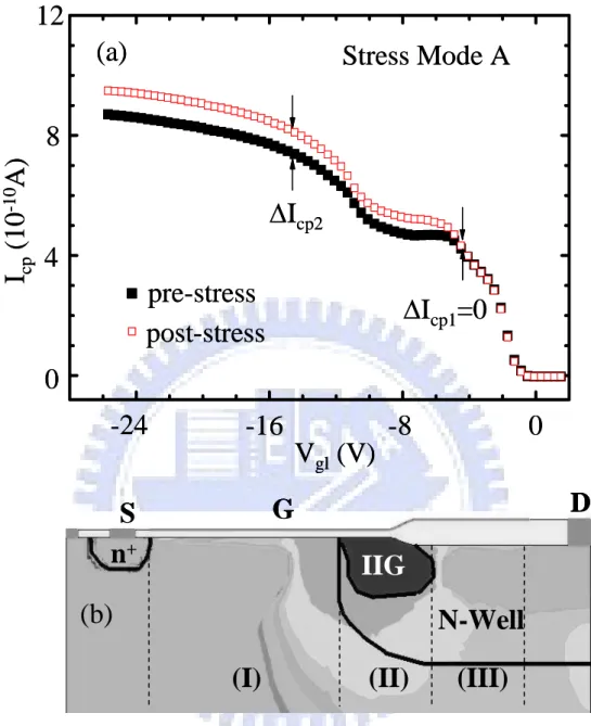
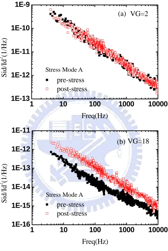
Fig. 2.6(a) shows the Icp in a fresh device and after 1400 sec. max. Ib stress (@Vg/Vd =8V/50V). The post-stress Icp in the first stage is nearly the same as the pre-stress one, indicating that region (I) oxide is not damaged by the stress. The post-stress Icp in stage 2, however, exhibits an upward shift while the flat-band voltage keeps the same (no rightward shift in the Icp). This feature suggests Nit generation in region (II) but no Qox creation. Numerical device simulation also shows the maximum IIG rate in region (II) (Fig. 2.6(b)). Although interface trap generation is observed from the Icp, the subthreshold swing of the device is not affected because the generated Nit is distributed in region (II). In addition, Idlin degradation is not observed either. Fig. 2.7(a) and (b) show the flicker noise of LDMOS in low Vg and high Vg measurement, respectively. A significant flicker noise increase is observed in high Vg measurement. Since gate voltage in high Vg measurement is higher than threshold voltage, the flicker noise would be mainly affected by interface state. Thus, an
increase flicker noise in Fig. 2.7(b) and no Idlin degradation are observed.
2.4.2 Vg~1/2Vd Stress Mode
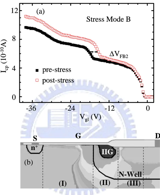
The Icp results before and after mode B stress (@Vg/Vd =30V/50V) are shown in Fig. 2.8(a). Nit generation in stress mode B is relatively small and can be realized due to a smaller substrate current (or a smaller IIG region in Fig. 2.8(b)), as compared to stress mode A. Unlike stress mode A, a distinct flat-band voltage shift in region (II) is noticed, which is manifested by a rightward shift of the Icp in stage 2. An arrow is drawn in Fig. 2.8(a) to indicate the flat-band voltage shift (ΔVFB2). The rightward shift of the slope is caused by negative Qox creation in region (II). As the stress time increase (Fig. 2.9), the slope in stage 2 keeps the same and ΔVFB2 versus stress time can be extracted. From the extracted ΔVFB2, the average Qox2 generation rate (Fig. 2.9) can be calculated by using the equation in section 2.2. Because of negative Qox creation, the resistance beneath the bird’s beak increases. At a large Vg, region (I) resistance is relatively small and the resistance in the bird’s beak region has a larger effect. Thus, Idlin degradation at a higher measurement Vg =40V is observed (Fig. 2.10). The flicker noise results before and after stress are shown in Fig. 2.11. Since Nit generation in region (II), the flicker noise also increases in high Vg noise measurement (Fig. 2.11(b)).
2.4.3 Max. Ig Stress Mode
Fig. 2.12(a) shows the Icp result before and after max. Ig stress (@Vg/Vd=50V/50V) for 1000 seconds. Significant Nit and Qox generation was noticed in region (I) and (II), respectively. It should be pointed out that a two-dimensional device simulation reveals that the IIG region splits into two parts (Fig. 2.12(b)); One is in the channel (region (I)) and the other is underneath the bird’s beak. Two different stress induced oxide
degradation mechanisms are noticed; One is Nit generation in region (I) and the other is negative Qox creation in region (II). These two trap creation processes are reflected by an upward shift of the first stage Icp denoted by ΔIcp1 and by a rightward shift of the second stage Icp (ΔVFB2 in Fig. 2.12(a)). In contrast to stress mode A, Nit generation occurs in region (I) rather than in region (II), which results in a significant subthreshold swing degradation (Fig. 2.13) in stress mode C. In addition, Qox2 creation results in a more serious Idlin degradation (Fig. 2.14) in mode C than in mode B. Note that the Idlin degradation in Fig. 2.14 is more apparent at a larger Vg. This is because the region (II) resistance occupies a larger part of the total resistance at a larger Vg.
The Nit1 and Qox2 growth rate in stress mode C are shown in Fig. 2.15 and Fig. 2.16, respectively. The growth rate obeys a power-law time dependence and the average power factor is around 0.25, which is in agreement with [11]. Due to oxide charge creation in region (II), a larger region (II) resistance results and the current flow in region (II) is pushed deeper into the substrate. Consequently, mobility exhibits a saturated effect and thus Idlin degradation shows a tendency to saturate in Fig. 2.17. This mobility saturation model is also described in [12,13] for MOSFET and [14] for LDMOS structure. By comparing mode A and B, the post-stress flicker noise exhibits an increase in Fig. 2.18(a) and (b) because of the Icp increase in channel region and Nit generation in accumulation region.
2.5
Summary
Drain current flicker noise degradation in various hot carrier modes is investigated. Max. Ib stress mode shows a significant flicker noise increase in drift region but no Idlin degradation. The increased flicker noise is attributed to the interface trap generation in drift region. Max. Ig stress mode shows a degradation of flicker noise in
both channel region and drift region because of interface trap generation in these regions. The Idlin degradation in max Ig stress mode is worse than max. Ib stress mode, which is attributed to the negative oxide charge creation in drift region. The LDMOS degradation behavior and trap properties in the three stress modes are summarized in Table 2.1.
S
n
+N-Well
D
n
+P-Well
G
(I) L
chan(II) L
acc(III) L
foxV
FB1V
FB2V
FB3(a)
V
ghV
gl(b)
V
T1V
T2V
T3I
n
+S
n
+N-Well
D
n
+P-Well
G
(I) L
chan(II) L
acc(III) L
foxV
FB1V
FB2V
FB3(a)
V
ghV
gl(b)
V
T1V
T2V
T3S
n
+N-Well
D
n
+P-Well
G
(I) L
chan(II) L
acc(III) L
foxV
FB1V
FB2V
FB3(a)
V
ghV
gl(b)
V
ghV
gl(b)
V
T1V
T2V
T3I
n
+I
n
+Fig. 2.1 (a) Cross-section of a metal contact n-LDMOS and corresponding flat-band (solid line) and threshold (dash line) voltage distribution. The device is divided into three parts, Lchan (channel region), Lacc
(accumulation region), and Lfox (field oxide region).
(b) Illustration of a charge pumping measurement wave form. The Vgh=12V is fixed and Vgl varies from +3.6 to -40V.
(a)
I
B(A)
10
20
30
40
50
V
g(V)
I
g(A)
mode A
mode B
mode C
W/L=20μm/3μm
@V
d=50V
Fig. 2.2 (a) Substrate current and gate current versus gate voltage in a LDMOS. Three different stress modes are shown in the figure, mode A (maximum Ib), mode B (Vg~1/2Vd), and mode C (maximum Ig).
(b) The bias conditions of the three stress modes.
0
I
B(A)
10
20
30
40
50
V
g(V)
10
20
30
40
50
V
g(V)
I
g(A)
mode A
mode B
mode C
W/L=20μm/3μm
@V
d=50V
30/50
B
50/50
C
8 /50
A
Vg/Vd
mode
30/50
B
50/50
C
8 /50
A
Vg/Vd
mode
(b)
0
0
12
10
8
6
4
2
0
I
cp(1
0
-10A)
-40
-32
-24
-16
-8
0
V
gl(V)
I
cp@ f=200kHz
D
S
L
foxL
accL
chanV
FB1V
FB2V
FB312
10
8
6
4
2
0
I
cp(1
0
-10A)
12
10
8
6
4
2
0
I
cp(1
0
-10A)
-40
-32
-24
-16
-8
0
V
gl(V)
-40
-32
-24
-16
-8
0
V
gl(V)
I
cp@ f=200kHz
D
S
L
foxL
accL
chanV
FB1V
FB2V
FB3Fig. 2.3 Typical CP current in a n-LDMOS. The three stages of the CP current correspond to the three regions of the device. The flat-band voltage of each region is indicated in the figure. The frequency in charge pumping measurement is fixed at 200 KHz.
0
5
10
15
20
25
30
35
40
0.0
0.5
1.0
1.5
2.0
Empty : MOS
Solid : LDMOS
2V
4V
6V
Vg=10V
8V
Low Vg
Id (mA)
Vd or Vk (V)
Fig. 2.4 (a) I-V characteristics in MOS and LDMOS at low gate voltage.
0
5
10
15
20
25
30
35
40
0
2
4
6
8
10
12
Vd or Vk (V)
Vg=16V
Id (A)
Vg=40V
High Vg
10
20
200
400
600
10
-2110
-2010
-1910
-18Vg=18V
Si
d (A
2/H
z)
Current in MOS / LDMOS (
μ
A)
LDMOS
MOS
(b)
Vg=2V
(a)
Fig. 2.5 Flicker noise in MOS and LDMOS at (a) low and (b) high gate voltage.
12
8
4
0
Fig. 2.6 (a) Charge pumping current versus Vgl before and after 1400 sec.
mode A stress. Upward shift of the Icp in stage 1 implies the
generation of interface trap in the accumulation region.
(b) Two-dimension device simulation of impact ionization (IIG) distribution in stress mode A.
I
cpA)
-24
-16
V
gl(V)
-8
0
Stress Mode A
(a)
ΔI
cp1=0
ΔI
cp2pre-stress
post-stress
-1 0(10
IIG
(II)
(I)
(III)
n
+N-Well
S
G
D
(b)
12
8
4
0
cpA)
-24
-16
V
gl(V)
-8
0
Stress Mode A
(a)
ΔI
cp1=0
ΔI
cp2pre-stress
post-stress
-1 0(10
I
IIG
(II)
(I)
(III)
n
+N-Well
S
G
D
(b)
IIG
(II)
(I)
(III)
n
+N-Well
S
G
D
(b)
1
10
100
1000
10000
1E-13
1E-12
1E-11
1E-10
1E-9
pre-stress
post-stress
VG=2
Fig. 2.7 (a) Low gate voltage and (b) High gate voltage flicker noise before and after mode A stress. The increase of high gate voltage flicker noise is caused by trap creation in the drift region.
Si
d/
(1
Fre
(a)
Stress Mode A
/Hz)
Id
2q(Hz)
1
10
100
1000
10000
1E-16
1E-15
1E-14
1E-13
1E-12
1E-11
pre-stress
post-stress
VG=18
Si
d/
Id
Freq(Hz)
(b)
Stress Mode A
/Hz)
2(1
I
cp(10
-1 0A)
pre-stress
post-stress
ΔV
FB2Stress Mode B
12
8
4
0
-24
-12
0
V
gl(V)
-36
(a)
G
D
S
(I)
(II)
(III)
n
+N-Well
IIG
(b)
I
cp(10
-1 0A)
pre-stress
post-stress
ΔV
FB2Stress Mode B
12
8
4
0
-24
-12
0
V
gl(V)
-36
(a)
G
D
S
(I)
(II)
(III)
n
+N-Well
IIG
(b)
Fig. 2.8 (a) Charge pumping current versus Vgl before and after 1400 sec.
mode B stress. The shift of the flat-band voltage in stage 2 implies the generation of negative oxide charge in the accumulation region. (b) Two-dimension device simulation of impact ionization (IIG) distribution in stress mode B.
Stress time (sec)
10
210
410
1210
11Δ
Q
ox2(/
cm
Fig. 2.9 Region (II) oxide trapped charge growth rate in stress mode B.
2
)
10
0Stress Mode B
Region (II)
10
210
410
1210
11Δ
Q
ox2(/
cm
2)
10
0Stress Mode B
Region (II)
I
dlind
egr
ad
ation
(
%
)
10
0.1
1
Stress time (sec)
10
210
410
0Stress Mode B
@V
g/V
d=40V/0.1V
I
dlind
egr
ad
ation
(
%
)
10
0.1
1
Stress time (sec)
10
210
410
0Stress Mode B
@V
g/V
d=40V/0.1V
Fig. 2.10 Linear drain current (Idlin) degradation rate measured at
1
10
100
1000
10000
1E-13
1E-12
1E-11
1E-10
1E-9
pre-stress
post-stress
VG=2
Fig. 2.11 (a) Low gate voltage and (b) High gate voltage flicker noise before and after mode B stress. The increase of high gate voltage flicker noise is caused by damage in the drift region.
Si
d/
(1
Fre
(a)
Stress Mode B
/Hz)
Id
2q(Hz)
1
10
100
1000
10000
1E-16
1E-15
1E-14
1E-13
1E-12
1E-11
pre-stress
post-stress
VG=18
Si
d/
z)
Freq(Hz)
(b)
Stress Mode B
(1/H
Id
212
8
4
0
I
cp(1
0
-10A)
-24
-12
0
V
gl(V)
-36
pre-stress
post-stress
ΔV
FB2Stress Mode C
16
ΔI
cp1(a)
G
D
S
(I)
(II)
(III)
n
+N-Well
IIG
(b)
12
8
4
0
I
cp(1
0
-10A)
-24
-12
0
V
gl(V)
-36
pre-stress
post-stress
ΔV
FB2Stress Mode C
16
ΔI
cp1(a)
12
8
4
0
I
cp(1
0
-10A)
-24
-12
0
V
gl(V)
-36
pre-stress
post-stress
ΔV
FB2Stress Mode C
16
ΔI
cp1(a)
G
D
S
(I)
(II)
(III)
n
+N-Well
IIG
(b)
Fig. 2.12 (a) Charge pumping current versus Vgl before and after 1000 sec.
mode C stress. Upward shift of the Icp in stage 1 indicates interface
trap generation in the channel region, and rightward shift of flat-band voltage in stage 2 implies oxide charge creation in the accumulation region.
(b) Two-dimension device simulation of impact ionization (IIG) distribution in stress mode C.
I
dFig. 2.13 Subthreshold characteristics before and after mode C stress. The swing degradation was attributed to interface trap generation in the channel region.
Fig. 2.14 Linear drain current versus Vg before and after mode C stress.
(A
)
10
-1010
-810
-60.8
1.2
1.6
V
g(V)
Fresh
Post mode C stress
@ V
d=0.1V
I
d)
10
-1010
-810
-60.8
1.2
1.6
V
g(V)
Fresh
Post mode C stress
@ V
d=0.1V
(A
0
10
20
30
V
g(V)
12
8
4
0
I
d(1
0
-5A)
16
Fresh
@V
d=0.1V
Post mode C stress
40
0
10
20
30
V
g(V)
12
8
4
0
I
d(1
0
-5A)
16
12
8
4
0
I
d(1
0
-5A)
16
Fresh
@V
d=0.1V
Post mode C stress
Stress Mode C
Stress time (sec)
10
210
410
010
1110
10ΔN
it 1(/cm
2)
Region (I)
10
9Stress Mode C
Stress time (sec)
10
210
410
010
1110
10ΔN
it 1(/cm
2)
Region (I)
10
9Fig. 2.15 Region (I) interface trap growth rate in stress mode C.
Stress time (sec)
10
210
410
1210
11Δ
Q
ox 2(/c
m
2)
10
0Region (II)
Stress Mode C
Stress time (sec)
10
210
410
1210
11Δ
Q
ox 2(/c
m
2)
10
0Region (II)
Stress Mode C
Stress time (sec)
10
110
210
310
410
1
I
dlinde
gra
d
at
io
n (%
)
Stress Mode C
I
dlin@V
g/V
d=40V/0.1V
Stress time (sec)
10
110
210
310
410
1
I
dlinde
gra
d
at
io
n (%
)
Stress Mode C
I
dlin@V
g/V
d=40V/0.1V
Fig. 2.17 Idlin degradation versus stress time in stress mode C. The
degradation is mainly caused by negative oxide charge creation in the drift region.
1
10
100
1000
10000
1E-13
1E-12
1E-11
1E-10
1E-9
1E-8
VG=2
pre-stress
post-stress
Fig. 2.18 (a) Low gate voltage and (b) High gate voltage flicker noise before and after mode C stress.
Sid/Id
2(1
z)
Fre
(a)
Stress Mode C
/H
q(Hz)
1
10
100
1000
10000
1E-16
1E-15
1E-14
1E-13
1E-12
1E-11
VG=18
pre-stress
post-stress
Sid/Id
2(1
/
z)
Freq(Hz)
(b)
Stress Mode C
H
Table 2.1
Idlin Isubthreshold Idlin N/A N/A N/A Device Deg. Region (II) Increase Nit Increase Qox Region (II) Increase Increase N/A N/A Noise Qox Nit N/A N/A Trap Property Region (II) Region (I) Region (I) Region (I) Trap Location C (50V/50V) B (30V/50V) A (8V/50V) Mode (Vg/Vd) Idlin Isubthreshold Idlin N/A N/A N/A Device Deg. Region (II) Increase Nit Increase Qox Region (II) Increase Increase N/A N/A Noise Qox Nit N/A N/A Trap Property Region (II) Region (I) Region (I) Region (I) Trap Location C (50V/50V) B (30V/50V) A (8V/50V) Mode (Vg/Vd)Chapter 3
Impact of Self-Heating Effect on
Hot Carrier Degradation
3.1 Introduction
Lateral diffused MOS (LDMOS) transistors have been widely utilized in today’s high-voltage/high-current drivers and RF power amplifiers [3,10]. High power consumption would increase heat generation in LDMOS and thus the self-heating effect (SHE) can be observed. SHE would significant affect the drain current and result in a negative output conductance [15]. Since LDMOS is subjected to AC stress rather than DC stress in certain applications, it is imperative to investigate the SHE on transient hot carrier degradation. To the purpose, we fabricate a special LDMOS structure, which incorporates a metal contact in the drift region. Thus, an internal voltage transient due to SHE can be probed directly.
Linear drain current (Idlin@Vg/Vd=40V/0.1V) is measured to monitor device degradation under AC or DC stress. A three-region charge pumping technique [16] is used to locate the damage area and corresponding trap properties. Two-dimensional device simulation is also performed to calculate impact ionization generation (IIG) rate in SHE and non-SHE conditions.
3.2 Self-Heating Effect
The setup for a transient measurement is shown in Fig. 3.1. A small resistance (10Ω) is arranged for the purpose of transient current measurement. The transient measurement of different device width and length is shown in Fig. 3.2. The SHE is
more serious in a larger (W/L) device due to a higher current density. Fig. 3.3(a) shows the normalized drain current (Id/W) versus Vd in small and large width devices under DC (Agilent 4156) measurement. The Id/W in linear region is nearly the same, indicating no process variations in these two devices. However, the larger width device exhibits a smaller Id/W in the saturation region. The reduction of the saturation current is attributed to self-heating caused mobility degradation. Fig. 3.3(b) further shows the Id/W in a DC and a fast transient measurement for a large width device. A larger Id/W is noticed in the transient measurement because of the elimination of SHE. A metal contact structure is used to probe the internal voltage (VI) near the bird’s beak, as shown in Fig. 3.4. Three-regions of a LDMOS are indicated, including channel region, accumulation region and field-oxide region. The contact is arranged in accumulation region with a n+ implant. Since the contact area is small enough that the device electrical characteristic would not be affected. A VI-Vg measured by DC (Agilent 4156) and a fast transient setup is shown in Fig. 3.5. Note that SHE is negligible in the fast transient measurement. A larger internal voltage in non-SHE condition is observed, which implies a stronger hot carrier stress in the channel region. The larger VI in a non-SHE condition is attributed to a higher mobility in accumulation region, and thus results in a smaller drift region resistance.
Fig. 3.6 shows a temperature distribution in LDMOS. Since the existence of field-oxide, heat could not be easily eliminated. Thus, field oxide region would exhibit a higher temperature distribution. Fig.3.6 also compared the temperature distribution in high Vg and low Vg operation. Since power consumption in high Vg is larger than in low Vg, a higher temperature can be observed. Fig. 3.7 shows the drain current increase versus power consumption. A linear function of power consumption is observed [17,18].
3.3 AC Hot Carrier Stress
Two stress modes (max. IB, and max. Ig) [16] are chosen in the study of the transient hot carrier degradation. The Ig-Vg and IB-Vg of a n-LDMOS are shown in Fig. 3.8 and corresponding stress modes are indicated. Fig. 3.9 shows the Idlin degradations in AC and DC stress conditions at the above two stress modes. Max. IB stress mode shows a slight difference in Idlin degradation between AC and DC stresses, implying that SHE is not important at a lower Vg stress. However, in max. Ig stress mode, AC stress shows more serious Idlin degradation than DC stress. Fig. 3.10(a) shows the Idlin degradation versus stress frequency at max. Ig stress. The Idlin degradation possesses a strong stress frequency dependence. The degradation increases with frequency and then becomes saturated. A corner frequency (f1=20 KHz) is indicated in Fig. 3.10(a). In addition, the duty cycle dependence of Idlin degradation is shown in Fig. 3.10(b). The Idlin degradation decreases from duty cycle=10% to duty cycle=100% (DC stress).
Fig. 3.11(a) shows a VI versus voltage pulse time. A SHE time constant is extracted to be around 5μs. We normalized the stress frequency and duty cycle dependence to on-sate stress time (=Duty cycle / frequency) and the correlation of them is shown in Fig. 3.11(b). The above result suggests that SHE becomes important as pulse time is longer than ~5μs.
3.4 Degradation Characteristics in AC/DC Stress
Max. Ig AC and DC stress are investigated in this section. A largest Idlin
degradation in AC stress phase is observed in Fig. 3.12 and corresponding Icp result is shown in Fig. 3.13. Two different stress induced oxide degradation mechanisms are indicated; one is the Icp1 increase in channel region and the other is VFB2 shift in accumulation region. By comparing the pre-stress and post-stress Icp, AC stress shows
more serious Icp1 increase and VFB2 shift than DC stress one. A two-dimensional device simulation is performed to calculate impact ionization rate with and without SHE (Fig. 3.14). The simulation also confirms that non-SHE condition (Fig. 3.14(b)) has a larger impact ionization rate.
Oscilloscope (Tektronix 5054)
Drift
HP4156
10 Ω
V
dV
IV
gV
sOscilloscope (Tektronix 5054)
Drift
HP4156
10 Ω
V
dV
IV
gV
sFig. 3.1 Measurement circuit setup for transient drain current and internal voltage (VI) measurement. The resistance (10Ω) is smaller than
0
2
4
6
8
10
12
14
16
18
20
22
1
2
3
4
5
6
7
8
9
10
Id (m
A)
Length(
μ
m)
W=20
μ
m, W=5
μ
m
Transient Meas.
DC Meas.
Vg/Vd=40V/40V
Fig.3.2 Comparison of drain current measured by Agilent 4156 (DC
measurement) and an oscilloscope (transient measurement) for different device widths and lengths at Vg/Vd=40/40.
0
2
4
6
DC Meas.
W=20
μ
m
W= 5
μ
m
Id
/
W (1
0
- 4A/
μ
m)
8.5%
0
10
20
30
40
0
2
4
6
W/L=20
μ
m/3
μ
m
DC Meas.
Transient Meas.
Vd (V)
8.4%
Id
/
W (1
0
-4A/
μ
m)
(b) (a)Fig. 3.3 (a) Normalized drain current versus drain voltage by DC
measurement for two different gate widths (b) Comparison of normalized drain current versus drain voltage by DC and transient measurements. The measurement Vg is 40V.
Fig. 3.4 The cross-section of a LDMOS and flat-band voltage distribution in each region. The metal contact (I) is arranged in the bird’s beak region with a n+ implant. This metal contact is small enough that width it would not affect the electrical characteristics of a LDMOS.
D
S
n
+N-Well
n
+P-Well
L
chanL
accL
foxn
+I
G
D
S
n
+N-Well
n
+P-Well
L
chanL
accL
foxn
+I
G
0
10
20
30
4
10
15
20
25
0
DC Meas.
Transient Meas.
V
I(V)
Vg (V)
Vd=40V
Fig.3.5 Internal voltage versus gate voltage in a LDMOS. An increase in an internal voltage is observed in the transient measurement.
6
4
2
0
0
3
6
9
300
360
420
480 T
em
p
er
at
u
re
(
K
)
X (
μ
m)
Y (
μ
m
)
L
acc+L
foxVg=40V
L
ch6
4
2
0
0
3
6
9
300
304
308
312
L
acc+L
foxT
em
p
er
at
u
re
(
K
)
X
(
μ
m)
Y (
μ
m)
Vg=10V
L
ch(a)
(b)
Fig.3.6 Simulation of temperature distribution in a LDMOS for (a) Vg=10V and (b) Vg=40V.
0.00 0.05 0.10 0.15 0.20 0.25 0.30 0.35 0.5 1.0 1.5 2.0 2.5 3.0 3.5 4.0 4.5
Δ
Id
/I
d
(100ms) (%)
power(W)
Vg(V)
10
20
30
40
W/L=20/3
0
10
20
30
40
50
Max. Ig
Max. Ib
@ Vd=50V
Vg (A)
I
g
(A)
I
B
(A)
Fig. 3.8 Substrate current and gate current versus gate voltage in a LDMOS.
Max.Ib
Max.Ig
0
4
8
I
dli nDegradation (%)
DC Stress
AC Stress
W/L=20
μ
m/3
μ
m
Fig.3.9 Idlin degradations in AC and DC stress conditions in max. Ib and
1
10
100
4
6
8
f
1Duty=10%
Stress Frequency (kHZ)
I
dlinD
egradation (
%
)
W/L=20
μ
m/3
μ
m
(a)
0.0
0.2
0.9
1.0
4
6
8
I
d linDegradat
ion (%)
Duty Cycle
Stress frequency
@ 20kHZ
(b)
Fig. 3.10 (a) Idlin degradation versus stress frequency. A transition
frequency is observed around f1=20kHz. (b)Idlin degradation
V
g
~5μs
V
I
V
o
lt
age
(V
)
10
20
30
40
0
20
40
60
80
100
Pulse Time (
μsec)
V
g
~5μs
V
I
V
o
lt
age
(V
)
10
20
30
40
V
o
lt
age
(V
)
10
20
30
40
0
20
40
60
80
100
Pulse Time (
μsec)
0
20
40
60
80
100
Pulse Time (
μsec)
(a)
1
10
100
1000
4
6
8
f
1Duty cycle=10%
Duty cycle=90%
Duty / frequency (
μ
sec)
I
dlinDeg
rad
ation (%)
(b)
Fig. 3.11 (a) The transient of an internal voltage (VI) for a gate pulse of
50μs with Vg/Vd=40V/40V. A decreasing VI is observed after a
heating time around 5μs.
(b) Idlin degradation versus on-state pulse time (=duty
cycle/frequency). The transition frequency (f1) in Fig. 3.10(a) is also indicated in the figure, which corresponds to an on-state pulse time of 5μs.
10
010
110
210
31
10
I
linFig. 3.12 Idlin degradation rate after max. Ig AC and DC stress. The stress frequency =20kHz and duty cycle=0.1.
d
Degradation (%)
Stress Time (sec)
AC Stress
DC Stress
L
fox-32
-24
-16
-8
0
0.0
0.4
0.8
1.2
1.6
Vgl (V)
Fresh
Post DC Stress
Post AC Stress
ΔV
FB2Δ
I
CP1Ic
p
(n
A)
D
S
L
accL
chanL
fox-32
-24
-16
-8
0
0.0
0.4
0.8
1.2
1.6
Vgl (V)
Fresh
Post DC Stress
Post AC Stress
ΔV
FB2Δ
I
CP1Ic
p
(n
A)
D
S
L
accL
chanFig.3.13 Threes region charge pumping measurement results after maximum Ig AC stress and maximum Ig DC stress. A flat-band voltage shift and an increased ICP are observed in accumulation region and in channel region, respectively.
(a)
w/i Self-Heating
IIG
(a)
w/i Self-Heating
IIG
(b)
w/o Self-Heating
IIG
(b)
w/o Self-Heating
IIG
Fig. 3.14 Two-dimensional device simulation of impact ionization generation (IIG) distribution (a) with heat flow analysis (corresponding to max. Ig DC stress mode) and (b) without heat flow analysis (corresponding to max. Ig AC stress mode). A larger IIG region is observed in both channel region and drift region.
Chapter 4
Conclusions
In Chapter 2, a three-region CP technique has been developed to characterize hot carrier stress induced oxide degradation in each region of a LDMOS. The trap location and property in various stress modes are identified and their impact on device characteristics has been evaluated. Our study reveals that the device subthreshold swing degradation is mainly affected by interface traps in the channel region while the linear drain current degradation is dictated by oxide trapped charge in the drift region. Low-frequency noise characterization is also performed to investigate the hot carrier stress effects. Our study shows that the low Vg and high Vg flicker noise are affected by channel region and drift region, respectively. In addition, max. Ig stress results in the worst hot carrier degradation in a LDMOS, which is attributed to both Nit generation in the channel region and Qox generation in the bird’s beak region.
In Chapter 3, the characterization of self-heating effect has been investigated. Self-heating effect on transient hot carrier behavior has been studied by measuring the internal voltage. The self-heating time (~5μs) is extracted. The max. Ig AC stress has the worst hot carrier degradation due to the elimination of self-heating effect. The charge pumping result shows that hot carrier degradations can be characterized by Icp1 increase (Nit generation) in the channel region and VFB2 shift (oxide charge creation) in the accumulation region.
Reference
[1] E. M. Sankara Narayanan, G. A. J. Amaratunga, W. I. Milne, J. I. Humphret, and Q. Huang, “Analysis of CMOS-Compatible Lateral insulated base transistors,” IEEE Transactions on Electron Devices, vol. 38, pp.1624-1632, 1991.
[2] Murari B. ‚“Smart power ICs,“ New York:Springer; 1995.
[3] D. Muller, A. Giry, F. Judong, C. Rossato, F. Blanchet, B. Szelag, A. Monroy Aguirre, R. Sommet, D. Pache, and O. Noblans, “ High-Performance 15-V Novel LDMOS TransistorArchitecture in a 0.25-μm BiCMOS Process forRF-Power Applications,“ IEEE Transactions on Electron Devices, vol.54, pp.861-868, 2007.
[4] B. Jayant Baliga, “An overview of smart power technology,” IEEE
Transactions on Electron Devices, vol. 38, pp.1568-1575, 1991.
[5] Claudio Contiero, Paola Galbiati, Michele Palmieri, Giulio Ricotti, and Roberto Stella, “Smart power approaches VLSI complexity,” Proceedings of
the International Symposium on Power Semiconductor Devices (ISPSD),
pp.11-16, 1998.
[6] P. L Hower and Sammeer Pendharkar, “Short and long-term safe operating area considerations in LDMOS transistors,” Proceedings of the International
Reliability Physics Symposium (IRPS), pp.545-550, 2005.
[7] B. J. Baliga, “High Voltage Integrated circuits”, IEEE Press, New York (1988) [8] J. G. Kassakian and D. J. Perreault, “The future of electronics in automobiles,”
Proceedings of the International Symposium on Power Semiconductor Devices (ISPSD), pp.15-19, 2001.
[9] Jongdae Kim, Tae Moon Roh, Sang-Gi Kim, Q. Sang Song, Dae Woo Lee, Jin-Gun Koo, Kyoung-Ik Cho, and Dong Sung Ma, “High-voltage power integrated circuit technology using SOI for driving plasma display panels,”
IEEE Transactions on Electron Devices, vol. 48, pp.1256-1263, 2001.
[10] Peter Moens, and Van Den Bosch, G, “Characterization of Total Safe Operating Area of Lateral DMOS Transistors,” Device and Materials
Reliability, IEEE Transactions on, vol. 6,pp.349-357, 2006.
degradation phenomena in lateral and vertical DMOS transistors,” IEEE
Transactions on Electron Devices, vol. 51, pp.623-628, 2004.
[12] J. S. Goo, H. Shin, H. Hwang, D. G. Kang, and D. H. Ju, “Physical analysis for saturation behavior of hot-carrier degradation in lightly doped drain n-channel metal-oxide-semiconductor field effect transistors,” Japanese Journal of
Applied physics, 33, pp.606-611, 1994.
[13] R. Dreesen, K. Croes, J. Manca, W. De Ceuninck, L. De Schepper, A. Pergoot and G. Groeseneken, “A new degradation model and lifetime extrapolation technique for lightly doped drain nMOSFETs under hot-carrier degradation,”
Microelectronics Reliability, 41, pp.437-443, 2001.
[14] N. Hefyene, C. Anghel, R. Gillon, M. ZEEE and A. M. Ionescu, ”Hot carrier degradation of lateral DMOS transistor capacitance and reliability issues,"
Proceedings of the International Reliability Physics Symposium (IRPS),
pp.551-554, 2005.
[15] K. A. Jenkins, J. Y. Sun, J. Gautier, “Characteristics of SOI FET’s under pulsed condition,” IEEE Trans. Elect. Dev., Vol. 44, Issue 11, pp. 1923-1930, Nov. 1997.
[16] C. C. Cheng, T.S. Hsieh, Tahui Wang,” Investigation of Hot Carrier Degradation Modes in LDMOS by using a Novel Three-Region Charge Pumping Technique,” Proceedings of the International Reliability Physics
Symposium (IRPS), pp.334-337, 2006.
[17] C. Anghel, A. M. Ionescu, N. Hefyene, R.Gillon, “Self–heating characterization and extraction method for thermal resistance and capacitance in high voltage MOSFETs,” IEEE Elect. Dev. Let., Vol. 25, Issue 3, pp.141-143, Mar. 2004.
[18] C. Anghel, R.Gillon, A. M. Ionescu, “Self-heating characterization and extraction method for thermal resistance and capacitance in HV MOSFETs,”