國
立
交
通
大
學
資訊學院 資訊學程
碩
士
論
文
指令快取記憶體的電源管理
-(對程式流程有感知能力的昏睡指令記憶體)
Power Management for Instruction Cache
-(Program Flow Sensitive Drowsy I-Cache)
研 究 生:周國維
指導教授:鍾崇斌 教授
指令快取記憶體的電源管理
Power Management for Instruction Cache
研 究 生:周國維 Student:Kuo-Wei Chou
指導教授:鍾崇斌 Advisor:Chung-Ping Chung
國 立 交 通 大 學
資訊學院 資訊學程
碩 士 論 文
A ThesisSubmitted to College of Computer Science National Chiao Tung University in partial Fulfillment of the Requirements
for the Degree of Master of Science
in
Computer Science August 2007
Hsinchu, Taiwan, Republic of China
指令快取記憶體的電源管理
學生:周國維
指導教授:鍾崇斌 博士
國立交通大學 資訊學院 資訊學程
摘
要
指令快取記憶體的電源管理,其只要的概論是將處於工作模式的快取列
的數量最小化。於是乎,在啟動的方案上,便是利用固定的目標位址使非
循序的快取列預先活躍化。在關閉的方案上,在某一快取列最後一次使用
並且將其內容物傳遞之後,此時便將此快取列關閉成昏睡模式。此概論的
目的便是將漏電所產生的能耗減少到最少。在開啟的階段,由於快取記憶
體的取代方案採用“關連性取代法”,如此導致會有好幾個的快取列同時活躍
化。在一段覺醒時間之後,除了會參考到的快取列,將其餘不會參考的快
取列切換成昏睡模式。這些額外增加的輔助硬體不只能提供下一個“基礎區
塊”的預測能力,並且當“錯誤的預測”發生後能導正程式的流程。在實驗的
結果顯示本論文建議的設計能減少的漏電能耗。當“覺醒潛在因素”是由一個
clock 的“覺醒時間”以及一個 clock1 本設計“電路延遲”。在一般的個例中,
執行時間會增加 10.898% 至 14.581% 已及減少 77.5% 知 82.4% 的漏電能
耗。
指令快取記憶體的電源管理
Power Management for Instruction Cache
student:Kuo-Wei Chou
Advisors:Dr. Chung-Ping Chung
Degree Program of Computer Science
National Chiao Tung University
ABSTRACT
Main concept of Power management of Instruction Cache - (Program Flow Sensitive Drowsy I-Cache (pfsDIC for brief)) is that minimize the numbers of active cache lines. So, on Turn-On scheme, utilize fixed Target address to preactivate the discontinuous Instruction Cache Line. On Turn-Off scheme, turn-off the cache lines after the last content of this cache line is transmitted. The purpose of such concept is to reduce maximum leakage energy. On Turn-On stage, there is several cache lines are activating due to low-way associated. After an amount of wakeup time, switch these awaken cache lines to “Drowsy mode” except to the referred cache line. The additional auxiliary hardware don’t only offer the predictive ability of next Basic Block, but also maintain the correct program flow when wrong prediction happens. The experiment results show the leakage reduction of proposed designs. When the wakeup latency is the sum of 1 clock of wakeup time and an extra 1 clock of circuit delay that caused by proposed design. In the average case, the Runtime increment is 10.898%~14.581% and the leakage reduction is 77.5% ~ 82.4%
誌
謝
首先感謝指導教授 鍾崇斌老師在學生就學期間给於學生耐心地教導與彈性又充 足的研討時間。再者感謝口試委員 單智君教授、王益文教授與陳德生教授願意擔任學 生的口試委員,並且在口試時的提供學生在研究上可以再改善的寶貴意見,使論文得以 修改得更完整以及完善。除此之外,感謝博士班的楊惠親學姊和喬偉豪學長在研究過程 中所給與的協助及幫助。 就一個在職生來說,我必須感謝公司主管潘正峰經理就學生在學期間在工作上的安 排,以及徐日明、閻學斌學長在學生修課時給予業界資料取得的協助,使得學生得以順 利地完成學業。 再次感謝 王益文老師以及第一次修習學分班〈多媒體影像處理〉 傅心家老師以及主管 潘正峰經理,在兩年前要考專班時惠賜推薦書,並感謝交大的在職專班讓我有再一次回 到校園學習的機會。 過去因為考試、作業、研究時常到深夜以致影響到家人的睡眠品質,在這裏衷心感 謝家人的體諒與支持。 周國維 2007.8.30
Table of Contents
Master of Science ... ii 摘 要 ... iii ABSTRACT ... iv 誌 謝 ... v Table of Contents ... viList of Figures... viii
List of Tables ... x
Chapter 1 Introduction... 1
1.1 Background... 1
1.1.1 DVS (Dynamic Voltage Scaling) ... 1
1.1.2 Characteristics of Program Execution ... 2
1.1.3 Dynamic branch predictor and its operation... 3
1.1.4 Basic Block... 7
1.1.5 Drowsy Caches: Simple Techniques for Reducing Leakage Power .... 8
1.1.6 Sub-bank Predictive I-Cache [5] ... 9
1.2 Research Motivation... 10
1.3 Research Objective ... 11
1.4 Organization of this Thesis... 12
Chapter 2 Design of Proposed Architecture ... 13
2.1 Challenges in Design ... 13
2.2 Design of BTB Side... 13
2.2.1 Extra component of BTB side ... 14
2.2.2 Update & Use of “BBSize” ... 16
2.2.3 Summary of BTB side ... 18
2.3 Design of Processor ... 21
2.3.1 Extra component on processor ... 21
2.3.2 Example for explain predictive instruction address ... 23
2.4 Design of Cache ... 27
2.4.1 Extra component (Preactivating Cache-Line FIFO)... 28
2.4.2 Extra component (Lines sensor) ... 29
2.4.3 Extra component (Lines sensor) ... 29
2.4.4 Extra component (Content Transmitter)... 30
2.4.5 Extra component (Stage Master) ... 31
3.1 Evaluation Methodology ... 33 3.2 Evaluation Metrics... 34 3.3 Experimental Environment... 35 3.4 Experimental Benchmark ... 36 3.5 Experimental Results... 38 3.6 Discussion... 46
3.6.1 Discussion with five evaluation metrics... 46
3.6.2 Important Considerations and/or Further Improvements ... 47
Chapter 4 Conclusion and Future work... 51
4.1 Conclusion ... 51
4.2 Future work ... 51
References ... 53
List of Figures
FIGURE 1.1LOGIC DIAGRAM OF DROWSY CACHE-LINE...2
FIGURE 1.2DIAGRAM OF BASIC BLOCK...7
FIGURE 1.3DIAGRAM OF SUB-BANK PREDICTION BUFFER...9
FIGURE 1.4DIAGRAM OF BASIC BLOCK...10
FIGURE 1.5DIAGRAM FOR DESCRIBING LOOKUP TIMING OF THIS THESIS...11
FIGURE 2.1DIAGRAM FOR DESCRIPTION OF “BBSIZE” FIELD EACH BTB ENTRY...14
FIGURE 2.2DIAGRAM FOR DESCRIPTION OF 2-DEPTH FIFO...15
FIGURE 2.3TRUTH TABLE OF “PREDICTION” FIELD AFTER VERIFY...16
FIGURE 2.4DIAGRAM FOR GATHERING “BBSIZE”. ...17
FIGURE 2.5DIAGRAM FOR USING “BBSIZE”...18
FIGURE 2.6A PIECE OF PROGRAM EXECUTION...19
FIGURE 2.7BLOCK DIAGRAM OF ORIGINAL ARCHITECTURE...20
FIGURE 2.8BLOCK DIAGRAM OF CPU CORE SIDE AND I-CACHE SIDE...22
FIGURE 2.9 THE DIAGRAM OF PIPELINE: THERE HAS 1 CIRCUIT DELAY,2 WAKEUP TIME...23
FIGURE 2.10TIMING DIAGRAM OF PREDICTIVE TARGET:...24
THERE HAS 1 CIRCUIT DELAY,2 WAKEUP TIME...24
FIGURE 2.11TIMING DIAGRAM OF WRONG PREDICTION...26
FIGURE 2.12GLOBAL VIEW OF CACHE SIDE...28
FIGURE 2.12BLOCK DIAGRAM OF “PREACTIVATING CACHE-LINE FIFO”...28
FIGURE 2.13BLOCK DIAGRAM OF “LINE SENSOR” AND “PREACTIVATING CACHE-LINE FIFO”. ...29
FIGURE 2.14LOGIC CIRCUIT DIAGRAM OF “CACHE-LINE”...30
FIGURE 2.15TRUTH TABLE OF “FUNCTION OPERATION” ...30
FIGURE 2.16LOGIC CIRCUIT OF “CONTENT TRANSMITTER”, WHEN TRANSMITTED FIRST CONTENT OF LINE.31 FIGURE 2.17DIAGRAMS OF TIMING AND RESOURCE...32
FIGURE 3.1SIMULATION FLOWCHART...36
FIG 3.2BLOCK DIAGRAM OF “RUNTIME INCREMENT” THAT AFFECTED BY “BTBINSERTION” AND “BBSIZE FIELD”. ...41
FIG 3.3BLOCK DIAGRAM OF “RUNTIME INCREMENT” THAT AFFECTED BY “CACHE SIZE”...41
FIG 3.4BLOCK DIAGRAM OF “RUNTIME INCREMENT” THAT AFFECTED BY “WORDS PER LINE”. ...42
FIG 3.5BLOCK DIAGRAM OF “RUNTIME INCREMENT” THAT AFFECTED BY “CACHE REPLACEMENT”...42
FIG 3.6BLOCK DIAGRAM OF “RUNTIME INCREMENT” THAT AFFECTED BY “WAKEUP LATENCY”. ...43
FIG 3.7BLOCK DIAGRAM OF “LEAKAGE ENERGY REDUCTION” THAT AFFECTED BY “BTB INSERTION” AND “BBSIZE FIELD”. ...44
FIG 3.9BLOCK DIAGRAM OF “LEAKAGE ENERGY REDUCTION” THAT AFFECTED BY “WORDS PER LINE” ...45
FIG 3.10BLOCK DIAGRAM OF “LEAKAGE ENERGY REDUCTION” THAT AFFECTED BY “CACHE REPLACEMENT” 45
FIG 3.11BLOCK DIAGRAM OF “LEAKAGE ENERGY REDUCTION” THAT AFFECTED BY “WAKEUP LATENCY”46
List of Tables
TABLE 3.1 SHOWS THE INSTRUCTION COUNTS, THE PERCENTAGE OF BRANCH INSTRUCTION AND MAXIMUM THE
BBSIZE...38
TABLE 3.2SIMULATION RESULTS OF PFSDIC(1) ...39
TABLE 3.3SIMULATION RESULTS OF PFSDIC(2) ...40
TABLE 3.4SIMULATION RESULTS OF SUB-BANKED...40
TABLE 3.5SIMULATION RESULTS OF SIMPLE TURN-OFF CACHE...40
Chapter 1 Introduction
The necessary of Power management of Instruction Cache is based on the following arguments: 1. the energy consumption of leakage is more important factor with process shrinking day by day. 2. Instruction cache always sends a content of instruction cache lines for CPU execution. 3. Should all parts of instruction cache lines be active?
Therefore, the thesis wants to implement an idea. The idea is that just only few numbers of cache lines are active and the other cache lines are drowsy by DVS (Dynamic Voltage Scaling) technique. And the number of active cache line is not more than number of “Way” that related to n-way associated replacement.
After equipping a filed that using for record the instruction number of this executing Basic Block (between the target address recorded in this BTB entry and next Branch instruction) in program execution. The next Target address will be calculated after the next instruction address of Branch instruction is calculated. Therefore, transmit the predictive program flow to Instruction Cache in advance; there will be avoid most Runtime increment due to the wakeup time of recharge.
Throughout this thesis, a classic MIPS five-stage pipeline is assumed. The five stages are Instruction fetch (IF) stage, Instruction decode/register fetch (ID) stage, Execution/effect address (EX) stage, Memory access (MEM) stage and Write-back (WB) stage respectively. The other assumption is the target address is confirmed on the “Instruction Decode” stage.
1.1 Background
1.1.1 DVS (Dynamic Voltage Scaling)
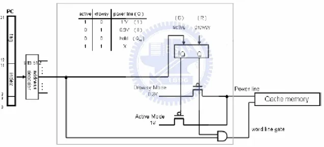
There often adopt multiple supply voltage (Dynamic Voltage Scaling) to reduce leakage power consumption. Reduce leakage energy using lower supply voltage, it provides 6x to 10x reduction over regular supply voltage. The method is often called “Drowsy mode”. If the cache line is at low leakage drowsy mode, its data is preserved but can not be accessed. Otherwise, the unchecked accesses to a drowsy line could
destroy its contents. The other thing, reactivate the cache lines need a small wakeup time.
Therefore, it is necessary to pre-activate what cache lines will be using in advance. It can avoid the penalty caused by waiting for wakeup time.
In the following figure shows a cache line that supports a drowsy mode. In order to support the drowsy mode, each cache line circuit includes two more transistors than traditional memory circuit. The voltage controller switches the cache line voltage between active and drowsy supply voltage depending on the drowsy bit. The word-line gating circuit is used to prevent accesses of the drowsy memory cells in the cache line, since the supply voltage of the drowsy cache line is far lower than the pre-charged bit-line voltage and thus unchecked accesses to a drowsy line could destroy its contents.
Figure 1.1 Logic diagram of Drowsy Cache-Line
Relationship with this thesis: there will be a similar circuit with each Instruction Cache Lines in the design of this thesis.
1.1.2 Characteristics of Program Execution
Now, let us analyze the character of program execution. Program execution can be classified into 2 categories:
1. Sequential execution:
This kind of execution occupies about 85-90% portion of program execution. 2. Execution of taken branches:
This kind of execution occupies about 10-15% portion of program execution. Taken branches can be further classified into 2 classes:
(1) Fixed target branches (75-97 % by simulation in table1):
Most taken branches are fixed target branches. Dynamic branch predictor like branch target buffer can handle fixed target branches with target expressed in immediate field of the instruction.
(2) Changing target branches:
It includes procedure return, some other special uses that load pc from a register other than link register (e.g., function table, switch conditional statement). Procedure return can be handled by return stack.
Relationship with this thesis: there shows that “Fixed Target Branch” occupies high percentage of the discontinuous execution. For simplicity, the thesis just focuses on “Fixed Target Branches” first.
1.1.3 Dynamic branch predictor and its operation
Due to reduce leakage power consumption, it need to decide which lines will be accessed in the near future and these are kept in the pre-activated state, and the rest of the lines are put into the low power drowsy mode. If the program execution is sequential, it is easy to pre-activate the cache lines considering the wakeup time. But, about 15% of instructions in typical programs are Taken-Branch. In order to reduce the extra penalty caused by wakeup time, dynamic branch predictor is often adopted.
Originally, dynamic branch predictor is used to help processor resolve the outcome of branch early, thus preventing control dependences from causing stalls [1]. The typical case of dynamic branch predictor is branch target buffer (BTB) [2]. Now, Branch target
buffer is used to offer predicting the path of the branch.
Branch target buffer is a branch prediction cache and is designed to reduce branch penalty by predicting the path of the branch and storing information about the branch. The major information stored in each entry of branch target buffer consists of:
1. Valid bit: to tell whether the entry is empty or not.
2. Branch instruction address (branch tag): the current program counter (PC) is compared to branch instruction address field to determine if there is a “hit”. 3. Branch target address: If there is a hit and the branch is predicted taken, the
program counter is loaded with this value and instruction fetching continues from this point.
4. Branch prediction bits (predictor): 2-bit prediction scheme is most commonly used [1].
For the classic MIPS five-stage pipeline, when the current program counter is sent to instruction memory to fetch the current instruction, this current program counter is also sent to branch target buffer to see if there is a “hit”.
If there is a “miss”, that means there is no valid entry whose branch tag equals the program counter, the instruction fetcher in CPU will update the program counter to the next sequential PC by adding a word size to the PC. There are 2 scenarios under a “miss”:
1. At the end of the ID stage for the branch instruction, it turns out that this is a not-taken branch :
The branch processing unit in CPU will not enter a new entry into branch target buffer for this branch, while the instruction fetcher in CPU will keep fetching the subsequent instruction.
The branch penalty in this case is 0 clock cycle.
2. At the end of the ID stage for the branch instruction, it turns out that this is a taken branch :
The branch processing unit in CPU will enter a new entry into branch target buffer for this branch, while the instruction fetcher in CPU will kill fetched instruction at IF pipe stage and start fetching the calculated branch
target address at the start of the next clock cycle. The branch penalty in this case is 1 clock cycle.
The detail of entering a new entry into branch target buffer is as follows:
If the position of the new entry is occupied, some replacement algorithm (e.g., Least Recently Used or Random algorithm) is used to discard an existing entry to make room for this new one.
In this new entry, valid bit field is set to 1, branch instruction address (branch tag) field is set to the branch instruction address (that is exactly the program counter 1 clock cycle ago), branch target address field is set to the value calculated at the end of ID stage, branch prediction bits field is set to the initialized value according to the adopted n-bit prediction scheme.
If there is a “hit”, that means there is a valid entry whose branch tag equals the program counter. There are 4 scenarios under a “hit”:
1. Branch prediction bits predicts this branch instruction is a taken branch, and at the end of ID stage for the branch instruction, it turns out to be a taken branch : At the end of the IF stage, branch target buffer will supply the branch target address to update the program counter. At the start of the next clock cycle, this corrected PC that is the branch target address is sent to instruction memory. At the end of the ID stage for the branch instruction, it turns out that the prediction 1 clock cycle ago is correct. The branch processing unit in CPU will update branch prediction bits in branch target buffer, while the instruction fetcher in CPU will keep fetching the subsequent instruction.
The branch penalty in this case is reduced to 0 clock cycle.
2. Branch prediction bits predicts this branch instruction is a taken branch, but at the end of ID stage for the branch instruction, it turns out to be a not-taken branch :
At the end of the IF stage, branch target buffer will supply the branch target address to update the program counter. At the start of the next clock cycle, this corrected PC that is the branch target address is sent to instruction memory. At the end of the ID stage for the branch instruction, it turns out that
the prediction 1 clock cycle ago is incorrect. The branch processing unit in CPU will update branch prediction bits of the branch entry in branch target buffer, while the instruction fetcher in CPU will kill fetched instruction at IF pipe stage, and start fetching the fall-through address after the branch instruction at the start of the next clock cycle.
The branch penalty in this case is 1 clock cycle.
3. Branch prediction bits predicts this branch instruction is a not-taken branch, and at the end of ID stage for the branch instruction, it turns out to be a not-taken branch :
At the end of the IF stage, branch target buffer will do nothing, the instruction fetcher in CPU will update the program counter to the next sequential PC by adding a word size to the PC. At the end of the ID stage for the branch instruction, it turns out that the prediction 1 clock cycle ago is correct. The branch processing unit in CPU will update branch prediction bits of the branch entry in branch target buffer, while the instruction fetcher in CPU will keep fetching the subsequent instruction.
The branch penalty in this case is 0 clock cycle.
4. Branch prediction bits predicts this branch instruction is a not-taken branch, and at the end of ID stage for the branch instruction, it turns out to be a taken branch :
At the end of the IF stage, branch target buffer will do nothing, the instruction fetcher in CPU will update the program counter to the next sequential PC by adding a word size to the PC. At the end of the ID stage for the branch instruction, it turns out that the prediction 1 clock cycle ago is incorrect. The branch processing unit in CPU will update branch prediction bits of the branch entry in branch target buffer, while the instruction fetcher in CPU will kill fetched instruction at IF pipe stage and start fetching the calculated branch target address at the start of the next clock cycle.
The branch penalty in this case is 1 clock cycle.
Summary for the interrelationship among BTB, instruction memory and CPU: 1. When an entry is found in branch target buffer and its prediction is taken,
2. When there is no entry found in branch target buffer or an entry is found but its prediction is not-taken, the instruction fetcher in CPU will update the program counter to the next sequential PC by adding a word size to the PC.
When a branch instruction is resolved at the end of ID stage, the branch processing unit in CPU will do the following things: updating branch target buffer (including entering a new entry or updating an existing entry) if necessary, flushing the instructions in the wrong path and updating the program counter when the current path is wrong.
Relationship with this thesis: in this thesis, there will be adding an extra field, that is using to record the instruction numbers of Basic Block, each BTB entries. On the other thing, the instruction numbers of Basic Block recorded in the field that is corresponding to the “Dynamic Branch Predictor”.
1.1.4 Basic Block
Basic Block is a straight-line code sequence with no branches in except to the entry and no branches out except at the exit. Therefore, Target1 is the entry of Basic Block, and Branch2 is the exit of Basic Block (Refer to Fig 1.2). For typical MIPS programs the average dynamic branch frequency is often between 15% and 25%, meaning that between four and seven sequential instructions execute between a pair of branch.
Relationship with this thesis: Because the design in this thesis wants to know the address pair is discontinuous in advance. And preactivate the discontinuous address an amount of wakeup time. So, the design in this thesis just use the character of Basic Block to predict next discontinuous address if somewhere record the instruction numbers of each Basic Block.
1.1.5 Drowsy Caches: Simple Techniques for Reducing
Leakage Power
There are two kinds of Turn-off policy: [4] 1. Simple Turn-Off policy:
Operation: Periodically (e.g.: 4K cycles) place all cache lines into drowsy mode.
Possible to improve:
(1) Some cache lines should not be turned off when period expires. (2) Too many Cache lines are active at same time.
2 Non-access Turn-Off policy:
Operation: Only the cache lines that have not been accessed during a fixed time period (e.g.: 32K cycles) are placed into drowsy mode.
Possible improve:
Some cache lines should be turning off early.
About Turn-on policy, both of above is turning on the cache line when accessed. Regardless of turn on policy or turn off policy, both of them operate cache line.
Relationship of this thesis: Simple Turn-Off policy will be adopted for comparison with the design of this thesis. And Simple Turn-Off policy let this thesis decide that turn off the cache line after last using.
1.1.6
Sub-bank Predictive I-Cache [5]
The following describes Turn-on and Turn-off policy of Sub-Banked Instruction Cache, respectively:
1. Turn-off policy:
Operation: Adopts a “Bank based strategy”, only one sub-bank is active at a time, while the rest of the sub-banks are in drowsy mode.
2. Turn-on policy:
There are two kinds of approach:
(1) Memory sub-bank prediction buffers: (Refer to Fig. 1.3)
Operation: Use a fully-associative buffer like BTB structure to pre-activate sub-bank.
Possible to improve: In particular, the CAM tag in the prediction buffers can consume significant amounts of dynamic power.
(2) Next sub-bank predictors in cache tags:
Operation: Extend cache tags to support next sub-bank prediction.
Possible to improve: Multiple next sub-bank addresses can not be kept when there are multiple transition addresses in a cache lines.
Regardless of turn on policy or turn off policy, both of them operate bank (e.g.: 4KB).
Figure 1.3 Diagram of Sub-bank Prediction Buffer
Relationship with this thesis: Because there are too many Instruction cache lines in a sub-bank, therefore, the design of this thesis hopes one cache line be the operating
element. And the design of this thesis still hopes to remain the predictive ability.
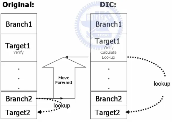
1.2 Research Motivation
“Dynamic Branch Predictor” offers the high accurate predictive direction of branch. And we know basic block is straight-line sequence with no branches in except to the entry and no branches out except at the exit. So, Target address / Fallthru address is the start of basic block, then next branch instruction in executing instruction is the end of basic block as Fig 1.4
Figure 1.4 Diagram of Basic Block
Assuming somewhere was storing the information of each basic block size. Adding an extra field to each BTB entry, the fields store the instruction numbers of the “Basic Block” after its Target / FallThrou address that corresponding to the prediction of “Dynamic Branch Predictor”.
If the field records the size of most Basic Block, we can achieve followings: 1. Avoid to lookup BTB each clock [6].
2. Easy to generate next branch address in advance.
Ex: “Branch2 address” = “size of Basic Block” + “Target1 address / FallThrou1 address”. (Refer to Fig 1.4)
3. Gain the predictive target address of next branch instruction by lookup BTB in advance.
Therefore, the predictive target address is generated before original several clocks. So, complete followings step by step (refer to Fig 1.5):
1. If Target2 address is calculated out on “EXE” stage of Branch1.
2. Transmits the target address to I-Cache side before using in pipeline wakeup time. 3. Equally, shift the other addresses of predictive sequential execution forward
wakeup time.
4. If complete all of above operation, then it can avoid the most wakeup latency.
Figure 1.5 Diagram for describing lookup timing of this thesis.
1.3 Research Objective
Because the target address can be predicted before several clocks, then the design of this thesis hope to transmit the predictive instruction address to I-Cache an amount of wakeup time ahead of CPU use.
Therefore, this thesis can achieve as followings:
1. Turn-On: Minimize the Runtime increment due to wakeup latency.
Scheme: Preactivates all predictive cache lines an amount of wakeup time ahead of use.
2. Turn-OFF: Minimize the leakage of active cache lines.
Scheme: Turn this cache line to “Drowsy” mode after the last content of this cache line is transmitted.
1.4 Organization of this Thesis
The rest of this thesis is organized as follows. Chapter 2 explains the design detail of power management of instruction cache. Chapter 3 presents evaluation methodology, experiment results and discussion. Conclusion and future works are then provided in Chapter 4.
Chapter 2 Design of Proposed Architecture
The design of power management of instruction cache is discussed in this chapter. Section 2.1 introduces challenges. Section 2.2, Section 2.3 and Section 2.4 introduce the design of BTB side, Processor side and Instruction Cache side respectively.
2.1 Challenges in Design
The following three point need to implement step by step: 1. Topic 1 (BTB side):
How to use the recorded instruction number of executing Basic Block to predict the target address of next branch instruction?
How to update “instruction numbers of Basic Block” when prediction of “Dynamic Branch Predictor” is changed?
2. Topic 2: (Processor) A. Instruction Address:
How to transmit the predictive target address on Instruction Address Bus an amount of wakeup time ahead of CPU use?
B. Instruction Data:
How to verify the correctness of content transmitted from I-Cache side? C. How to handle “Wrong Prediction”?
3. Topic 3: (Cache)
When to change the supply voltage of I-Cache line?
The moment is between the two addresses which content place in different cache lines.
2.2 Design of BTB Side
The Goal for resolve topic1 of design challenge:
1. Gather the “instruction numbers of each Basic Block” (“BBSize” for brief) corresponds to the prediction of “Dynamic Branch Predictor”.
2. Using “BBSize” to predict the target address of next (predicted) taken-branch instruction.
So, there needs to increase some extra components and describes them briefly:
1. Create one / two extra field to each BTB entry for record “BBSize” of each Basic Block.
2. A counter to count the “instruction number of each Basic Block”. 3. A mechanism for update and operation of BBSize.
2.2.1 Extra component of BTB side
Now, let’s describe the extra components:
1. Adding one BBSize Field each entry of BTB:
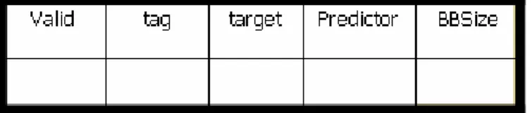
(1) Valid, Tag, Target and Predictor: same as originals of BTB. (2) BBSize:
A. Record the numbers of instruction after target of this entry.
B. One field for just prediction / two field for both decision (decide by simulation) need to record.
Figure 2.1 Diagram for description of “BBSize” field each BTB entry
Why does there create two fields each BTB entry? Because there maybe two conditional address after each Branch instruction. The two addresses are: 1.Target address when Branch-Taken. 2. FallThrou address when Branch Not-Taken. Therefore, the BBSize will be changing when the prediction of “Dynamic Branch Predictor” is changed and just one “BBSize ” field each BTB entry. The decision will be show you on later result of simulation.
2. Adding a BBCounter: Count the instruction passed after previous Branch instruction. And its operations are (1) INC when Branch instruction doesn’t meet. (2) CLR when Branch instruction meets.
3. Adding a 2-depth BBFIFO. The FIFO has two level elements: (1) Top element records the information for update “BBSize” of top “BTBIndex” field point to. (2) Bottom element records the information for record BTB index and prediction of next Branch instruction.
Figure 2.2 Diagram for description of 2-depth FIFO
The field description of this FIFO:
(1) BTBIndex: using for records the index of BTB entry. (2) Prediction: there are two condition:
A. Before verification of prediction: Record the prediction of branch instruction.
B. After verification of prediction: Indicate operation of BBCounter and BBSize update. (refer to fig 2.3)
(A) When predictor is correct and BBSize isn’t NULL. Then the field sets “Freeze” that represents “BBCounter” doesn’t work, “BBSize” doesn’t need to update.
(B) When predictor isn’t correct and it changes prediction. Or “BBSize” is NULL. Then the field sets “Update” that represents
“BBcounter” work, “BBSize” needs to update.
Figure 2.3 Truth Table of “Prediction” field after verify
2.2.2 Update & Use of “BBSize”
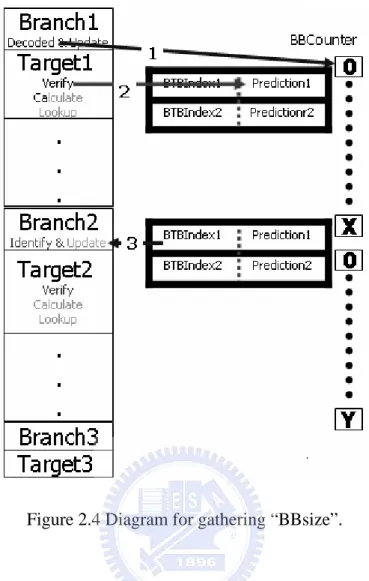
Now, start to describe how to gather and record “BBSize” step by step: (refer to fig 2.4)
1. BBCounter set 0 after branch decoded.
2. After making sure the program flow is Target1, a) Update “Prediction1”.
b) Pop the BBFIFO c) Clear the FIFO bottom.
3. Update “BBSize1” by “BTBIndex1”, “Prediction1” and “BBcounter”. 4. Goto 1.
Figure 2.4 Diagram for gathering “BBsize”.
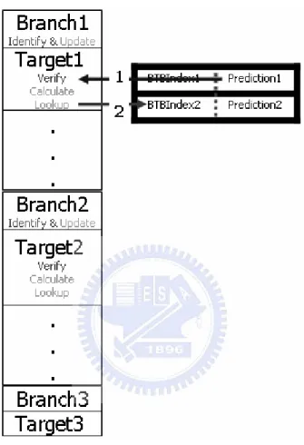
Now, start to describe how to use above components to gain the predictive Target address of next Branch instruction in execution.(refer to fig 2.5)
1. After making sure the program flow is Target2, (1) Update “Prediction2”.
(2) Pop the BBFIFO (3) Clear the FIFO bottom. 2.
(1) Calculation:
A. BBSize isn’t NULL.
-> Calculate the Branch2 address using adding Target1 address and BBsize1.
B. BBSize is NULL
(2) Lookup:
A. Just one time to Branch2. B. Each instruction until Branch2.
(3) Record the index of BTB entry that lookup out by Branch2 address. 3. Goto 1.
Figure 2.5 Diagram for using “BBsize”.
2.2.3 Summary of BTB side
In fact, there has a two kind of penalty when using Drowsy Instruction Cache. First, the performance loss is where needs some adding wakeup time to preactivate the drowsy line that will be using. Second, the energy overhead due to recharge for switch the instruction cache line from “Drowsy mode” to “Active Mode”.
Therefore, the purpose of the design is transmit the instruction address to I-Cache an amount of wakeup time ahead of CPU use. It is impossible to transmit all of correct
instruction address. Because the sequential program execution is just only about 85%. So, there need to handle when branch-taken happens on the program flow.
The solution of branch instruction handle is using BTB. But there need to generate the next predictive target address an amount of wakeup time ahead of use. Therefore, the design adds an extra field to each BTB entry. The field records the instruction numbers after its target. The purpose of the fields is that to calculate the next branch instruction address. Then using the result of previous calculation to lookup BTB and gain the next predictive target address ahead several clocks. How much the clocks are? The answer is relating to the instruction numbers that are after executing target.
Using Figure 2.6 to explains, if Branch1 is decoded in “Instruction Decode” stage, and Traget1 is Branch1 consecutive execution. Assume the execution between Target1 and Branch2 are sequential instructions. As previous description in chapter 1.1.4, basic Block is a straight-line code sequence with no branches in except to the entry and no branches out except at the exit. According the definition of Basic Block, it can say the executions between Target1 and Branch2 are in a same “Basic Block”.
Figure 2.6 A piece of program execution
So, if Target1 is fetch due to “Dynamic Branch predictor” and BTB, and somewhere has the instruction numbers (the size of Basic Block) after Target1. At this
moment, Branch2 address can easy be calculated by adding Target1 address and the instruction numbers. Target2 address is generated by using the result of calculation to lookup BTB.
After Target1 was calculated by CPU, you things where increase an extra action of lookup BTB for Target2. In this way will increase one more time action of lookup BTB. The answer is NO; there decrease the times of lookup BTB. (use Figure 2.7 to explain) In original architecture, there need to lookup BTB each clock. In the thesis, there don’t lookup BTB from the next execution of Targe1 until meeting Branch2. Because of there have the information of instruction numbers after Target1. The information shows us how much sequential instruction after Target1. The action of lookup BTB can be omitted, because the execution is sequential instruction. The other thing, the design in this thesis just moves the action of lookup BTB in original architecture until after Target1 instruction.
Figure 2.7 Block diagram of original architecture
The design in the thesis, there will predict the subsequent execution of Branch2 always continuous in following several conditions (still using figure 2.7 to explain):
2. There is no information of instruction numbers after Target1. 3. Branch2 is not gathered into BTB.
4. The “Dynamic Branch Predictor” of Branch2 predict Branch-Not-Taken”.
2.3 Design of Processor
Finish the description of predictive target address. The goal of design is: 1. Transmits all predictive address an amount of wakeup time ahead of use. 2. Verify the correctness of prediction wakeup time ago.
3. Handle the “Wrong Prediction”.
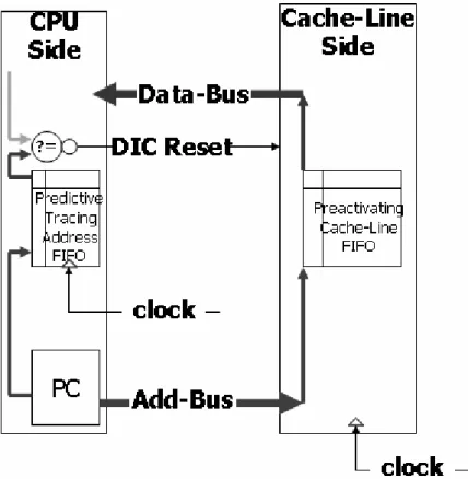
2.3.1 Extra component on processor
Therefore, there creates extra FIFO on the CPU side and cache side, respectively. They are named as “Predictive Tracing Address FIFO” (PTA_FIFO for brief) and “Preactivating Cache-Line FIFO” (PCL_FIFO for brief).
Figure 2.8 Block diagram of CPU core side and I-Cache side
Now, describes the operation of extra FIFO. First, the operation of Predictive Tracing Address FIFO: 1.Push the predictive PC to PTA_ FIFO bottom each clock. 2. Clear whole PTA_FIFO when Wrong Prediction. Then, describes the operation of Preactivating Cache-Line FIFO: 1.Push the address from “Instruction Address BUS” to PCL_FIFO bottom each clock. 2. Clear whole PCL_FIFO when Wrong Prediction.
Actually, the depth of the two FIFO is designed as “wakeup time + 1”. On CPU side, The “Predictive Tracing Address FIFO” (PTA_FIFO) is using for verify the correctness of predictive address wakeup time ago. On the Cache side, the “Pre-activating Cache-Line FIFO” (PCL_FIFO) has two conditions to explain: 1. the top of PCL_FIFO is using for make sure that cache line of address referred is activated. 2. The bottom of PCL_FIFO is using for indicate the timing that switch the cache line to “Drowsy mode”.
Summary of the two FIFO, the address on top of “PTA_FIFO (on CPU side)” is just the address of the content that transmitting from Cache-Line now. Therefore, compares the two address of top of “Predictive Tracing Address FIFO” (PTA_FIFO) and
calculated address on “ID” stage now. If the two addresses are not same, the “DIC reset” will be asserted. Because it represents the prediction wakeup time ago is wrong.
2.3.2 Example for explain predictive instruction address
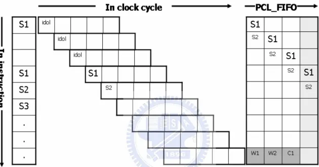
Now, take some example to explain more clearly. First, show you the timing diagram of initialization.
Figure 2.9 the diagram of Pipeline: there has 1 circuit delay, 2 wakeup time
In fig 2.9, the left blocks are represents the address executes in instruction. The middles represent the pipeline stage. And the right blocks is represents the address in PCL_FIFO, left is the bottom of FIFO and right is top of FIFO.
About S1, S2… and SX, the ‘S’ represent the sequential instruction. About W1 and W2, the ‘W’ represents wakeup time. Therefore, “W1” represents the cache line of the address referred is preactivated 1 cycle. About “C1”, it represents one cycle circuit delay. The circuit delay is the latency of extra mechanism in instruction cache side, and explains on next chapter in detail.
Now, start to explain
through Instruction Address Bus to the bottom of “PCL_FIFO”. And the top of “PCL_FIFO” is NULL. Therefore, the pipeline is idol.
2. Second cycle (second row) of fig 2.9. First, “S2” is transmitted from CPU side through Instruction Address Bus to the bottom of “PCL_FIFO”. So, “S1” pop one level to “W2”, it is say the Cache line that “S1” referred is preactivated one clock. And the top of “PCL_FIFO” is NULL. Therefore, the pipeline is idol.
3. Similar as 2.
4. Forth cycle (forth row) of fig 2.9. First, “S4” is transmitted from CPU side through Instruction Address Bus to the bottom of “PCL_FIFO”. At the moment, “S1” pop to the top of “PCL_FIFO”, it is say the Cache line that “S1” referred is preactivated 3 clocks and the Cache line is active. And the top of “PCL_FIFO” is not NULL. Therefore, the pipeline isn’t idol, the “S1” is fetched into “IF” stage.
From this example, it let us know there will be three unit of latency when the timing of initialization.
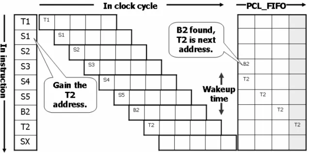
Continuously, introduce the timing of predictive target address. (Refer to the fig 2.10)
Figure 2.10 Timing diagram of predictive target: There has 1 circuit delay, 2 wakeup times
In fig 2.10, about B2, the ‘B’ represents the Branch instruction. About T2, the ‘T’ represents the Target instruction.
Now, start to explain from forth cycle:
1. Forth cycle (forth row) of fig 2.10. First, “B2” is transmitted from CPU side through Instruction Address Bus to the bottom of “PCL_FIFO”. And assume the top of “PCL_FIFO” doesn’t NULL. Therefore, the pipeline isn’t idol. 2. Fifth cycle (Fifth row) of fig 2.10. Because “B2” meets, therefore, the next
address is predicted as “T2” due to the prediction of “Dynamic Branch Predictor”. So, “T2” is transmitted from CPU side through Instruction Address Bus to the bottom of “PCL_FIFO”. So, “B2” pop one level to “W2”. And assume the top of “PCL_FIFO” doesn’t NULL. Therefore, the pipeline isn’t idol.
3. Assume sixth cycle and seventh cycle don’t meet Branch instruction. Therefore, the “PCL_FIFO” is just pop one element each clock.
4. Eighth cycle (eighth row) of fig 2.10. At the moment, “T2” pop to the top of “PCL_FIFO”, it is say the Cache line that “T2” referred is preactivated 3 clocks and the Cache line is active. Therefore, the pipeline isn’t idol, the “T2” is fetched into “IF” stage.
From this example, it let us know where will not be occurred any performance loss when the prediction of “Dynamic Branch Predictor” is correct.
Continuously, introduce the timing of predictive target address. (Refer to the fig 2.11)
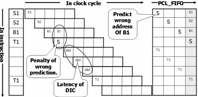
Figure 2.11 Timing diagram of wrong prediction
Now, start to explain from first cycle:
1. First cycle (first row) of fig 2.11. Because “B1” meets, therefore, the next address is predicted as “S” due to the prediction of “Dynamic Branch Predictor”. So, “S” is transmitted from CPU side through Instruction Address Bus to the bottom of “PCL_FIFO”. And assume the top of “PCL_FIFO” doesn’t NULL. Therefore, the pipeline isn’t idol.
2. Assume second cycle and third cycle don’t meet Branch instruction. Therefore, the “PCL_FIFO” is just pop one element each clock.
3. Forth cycle (Forth row) of fig 2.11. At the moment, “S” pop to the top of “PCL_FIFO”, it is say the Cache line that “S” referred is preactivated 3 clocks and the Cache line is active. Therefore, the “S” is fetched into “IF” stage. After the calculation of “B1” on “ID” stage, the calculated address isn’t same as the address of “S”. Therefore, the status of “IF” stage will be refreshed. And this penalty is original architecture. On the other hand, the whole “PCL_FIFO” will be cleared when each “Wrong Prediction” occurs.
4. 5th cycle (5th row) of fig 2.11. “T1” is transmitted from CPU side to I-Cache side through Instruction Address Bus. And “T1” is transmitted to the bottom of “PCL_FIFO” when I-Cache received the address form Instruction Address Bus.
And the top of “PCL_FIFO” is NULL. Therefore, the pipeline is idol.
5. 6th and 7th cycle are similar. Assume there don’t meet Branch instruction., therefore, the “PCL_FIFO” is just pop one element each clock. And the top of “PCL_FIFO” is NULL. Therefore, the pipeline is idol.
6. Eighth cycle (eighth row) of fig 2.11. At the moment, “T1” pop to the top of “PCL_FIFO”, it is say the Cache line that “T1” referred is preactivated 3 clocks and the Cache line is active. Therefore, the pipeline isn’t idol, the “T1” is fetched into “IF” stage.
From this example, it let us know where will be occurred performance loss when the prediction of “Dynamic Branch Predictor” is wrong. And there will be 1 penalty of “Wrong Prediction” and additional latency according to wakeup time and circuit delay.
2.4 Design of Cache
The goal of I-Cache side is that operates power management of I-Cache line. And there includes two status: 1.Turn-on (By PCL_FIFO bottom) status, when the first words of Cache Line meets, therefore, activate all cache line that address maybe refer to. 2. Turn-off (By PCL_FIFO top) status: (1) first content of this cache line, turn-off all Cache line except to address refer to.(2) Last content of this cache line, turn-off all Cache Line that address refer to.
Another goal of I-Cache side is that transmits the content corresponding to the address transmitted from CPU side an amount of wakeup time ago.
Figure 2.12 Global View of Cache side
2.4.1 Extra component (Preactivating Cache-Line FIFO)
Preactivating Cache-Line FIFO:
The numbers of PCL_FIFO is corresponding to “Wakeup time + 1”. Each element includes two fields:
1. Address:
Records the address from “Instruction Address Bus” and pop one element each clock
2. 3 kind of stage in the field of “Word location”: ‘0’: First word (Head) of Cache line
‘1’: last word (Trail) of Cache line ‘2’: mediums of Cache line
2.4.2 Extra component (Lines sensor)
Lines sensor responds to compares the addresses of two most bottom elements. And there are two kinds of condition: (refer to fig 2.13)
1. Equal: set their “Word location” is ‘2’ (medium).
2. Not equal: set most bottom one is setting to “0” (Fist content of cache line), above one is setting to ‘1’. (Last content of cache line)
Figure 2.13 Block diagram of “Line sensor” and “Preactivating Cache-Line FIFO”.
2.4.3 Extra component (Lines sensor)
There needs to create voltage switcher for switch the work voltage each Cache line. In Figure2.14, extra create a multiplexer for different operation and the multiplexer is controlled by the signal that named “Function Operation” (Fun_OP for brief)
Figure 2.14 Logic circuit diagram of “Cache-line”.
Power Manager: using “Word Location” of element to operate the following two stages sequentially: (Refer to fig2.15)
1. ON stage: get the bottom element of FIFO.
When the field of “Word Location” is ‘0’ (Head, First content of cache line), turn-on all Cache line (Fun_OP1) that referred by “Address”.
2. OFF stage: get the top element of FIFO.
(1) When the field of “Word Location” is ‘0’ (Head, First content of cache line), turn-off all Cache line (Fun_OP0) except to address refer to.
(2) When the field of “Word Location” is ‘1’ (Trail, Last content of cache line), turn-off all Cache Line (Fun_OP1) that address refer to.
Figure 2.15 Truth table of “Function Operation”
2.4.4 Extra component (Content Transmitter)
Content Transmitter is using the data in Top of PCL_FIFO:
1. When the “Word Location” is ‘0’ (Head, First content of cache line), transmits the hit content and record the hit way number to “Way #”.
cache line), merge “Way #” and index to transmit the referred content.
Figure 2.16 Logic circuit of “Content Transmitter”, when transmitted first content of Line.
2.4.5 Extra component (Stage Master)
Stage Master has two jobs to work:
1. Indicate other modules works or idol. 2. Avoid any two modules use same resource.
The fig2.17 describes two things: The one clock of circuit delay is using for assign the sub-module in different stage. There are three stages in one clock and there are three resources in I-Cache side. The three kinds of resources are “Word Location in FIFO”, “Address in FIFO” and “Way number” (Way # for brief).
Chapter 3 Evaluation and Discussion
Proposed designs in Chapter 2 are evaluated by trace-driven simulator. The benchmark suit is a subset of MiBench [7], which is a benchmark suite for embedded programs. The results are evaluated by two metrics: Runtime increment and Leakage energy reduction.
3.1 Evaluation Methodology
Since proposed designs in Chapter 2 are system-level innovation in computer architecture, behavioral simulation like trace-driven simulator can be a suitable approach to prove how many benefits such innovation gains compared with “Simple Turn-Off Cache” and “Sub-Banked Instruction Cache”.
Proposed designs are evaluated by a trace-driven simulator. Since proposed designs in this thesis are based on classic MIPS five-stage pipeline, my simulator uses MIPS I instruction trace as key input.
My trace-driven simulator accepts the following parameters as its input configuration: 1. On BTB Side:
(1) The two condition of BTB insertion: A. All Branch can insert the BTB
B. Taken Branch only can insert the BTB. (2) The number of BBSize field each BTB entry:
A. One BBSize field each BTB entry. B. Two BBSize field each BTB entry. 2. On Cache Side:
(1) The scheme of “Cache Replacement”: A. Direct mapping.
C. 4-Way associated.
(2) The scheme of “Cache Size”: A. 8KB
B. 16KB C. 32 KB D. 64KB. E. 128 KB.
(3) The scheme of “Words per Cache Line”: A. 4 Words per cache line.
B. 8 Words per cache line. C. 16 Words per cache line.
(4) The scheme of “Wakeup time” for the recharge of cache line:
A. 2 wakeup latency for the proposed design: 1 wakeup time + 1 circuit delay. B. 3 wakeup latency for the proposed design:2 wakeup time + 1 circuit delay. C. 5 wakeup latency for the proposed design:4 wakeup time + 1 circuit delay.
There are two statistics of experiment results : 1. Runtime increment.
2. Energy Requirement.
3.2 Evaluation Metrics
In this thesis, the following metrics are used to evaluate proposed designs of pfsDIC:
1. Runtime Increment The equation is
Runtime increment = The Execution cycles of proposed design / The Execution cycles of Non-Drowsy mechanism
2. Energy Requirement The equation is
Energy consumption = energy consumption per clock * execution cycle.
Energy consumption per clock = drowsy bits * C1 + active bits * C2 (C1:C2 = 0.16: 1) [4]
3.3 Experimental Environment
The experimental toolset MIPS SDE / MIPS FGT 5.02.02 [8] is used to generate MIPS I instruction trace for benchmark programs:
1. Install MIPS SDE / MIPS FGT 5.02.02.
2. Use command “sde-make SBD=GSIM1B” to build MIPS I code (benchmark_ram) of benchmark program for GNU simulator platform.
3. Use command “sde-run --trace-insn=on --trace-file trace_filename
benchmark_ram” to generate MIPS I instruction trace file.
Since delay branch slot is always applied in GNU simulator platform, the generated trace file needs to be modified to remove delay branch slot for all branch and jump instructions.
The modified trace file is then fed into trace simulator by specifying various parameters like BTB configuration. Figure 3.1 shows the flowchart of simulation.
Figure 3.1 Simulation flowchart
3.4 Experimental Benchmark
The benchmark programs selected are a subset of MiBench [8], which is a benchmark suite consisting of commercially representative embedded programs. MiBench consists of 6 categories including Automotive and Industrial Control, Network, Security, Consumer
Devices, Office Automation, and Telecommunications. In each category, at least one benchmark is chosen as experimental benchmark. All chosen benchmarks are listed as below:
1. In the category of Automotive and Industrial Control
Basicmath: it performs simple mathematical calculations that often don’t have
dedicated hardware support in embedded processors.
Bitcount: it tests the bit manipulation abilities of a processor by counting the
number of bits in an array of integers. 2. In the category of Network
Dijkstra: it constructs a large graph in an adjacency matrix representation and then
calculates the shortest path between every pair of nodes using repeated applications of Dijkstra’s algorithm.
3. In the category of Security
Sha: it is the secure hash algorithm that produces a 160-bit message digest for a
given input. It is often used in the secure exchange of cryptographic keys and for generating digital signatures.
Rijndael encrypt/decrypt: Rijndael was selected as the National Institute of
Standards and Technologies Advanced Encryption Standard (AES). It is a block cipher with the option of 128-, 192-, and 256-bit keys and blocks.
4. In the category of Consumer Devices
Jpeg encode/decode: JPEG is a standard, lossy compression image format. It is a
representative algorithm for image compression and decompression and is commonly used to view images embedded in documents.
Lame: it is a GPL'ed MP3 encoder that supports constant, average and variable
bit-rate encoding. It uses small and large wave files for its data inputs. 5. In the category of Office Automation
Stringsearch: it searches for given words in phrases using a case insensitive
comparison algorithm.
6. In the category of Telecommunications
FFT/IFFT: it performs a Fast Fourier Transform and its inverse transform on an
frequencies contained in a given input signal.
ADPCM encode/decode: Adaptive Differential Pulse Code Modulation (ADPCM)
is a variation of the well-known standard Pulse Code Modulation (PCM). A common implementation takes 16-bit linear PCM samples and converts them to 4-bit samples, yielding a compression rate of 4:1.
CRC32: it performs a 32-bit Cyclic Redundancy Check (CRC) on a file. CRC
checks are often used to detect errors in data transmission.
Table 3.1 shows the instruction counts, the percentage of Branch instruction and Maximum the BBSize.
3.5 Experimental Results
Table 3.2 shows simulation results. The abbreviations on table 3.2 are listed as below. There are 3 kinds of designs to evaluate and show their experiment results :
1. The design of the thesis : with all kinds of configuration. 2. Sub-Banked Design: With last four kinds of configuration. 3. Simple Turn-Off Design: With last four kinds of configuration.
1. The policy of BTB insertion.
2. The numbers of BBSize field each BTB entry. 3. Cache Size.
4. Words per cache line.
5. The scheme of Cache replacement. 6. Wakeup latency.
And the simulation bases on the basic configuration as followings. There changes one setting of configuration each evaluation. The experiment results show you in Table3.2, Table3.3, Table3.4 and Table3.5.
Basic configuration shows as below:
1. The scheme of BTB insertion: All branches.
2. The number of BBSize field: one “BBSize” field each BTB entry. 3. Cache Size: 32KB.
4. Words per Line:16 Words per cache line.
5. The scheme of Cache replacement: Direct mapping.
6. Wakeup latency: 1 clock wakeup time + 1 clock circuit delay.
Table 3.3 Simulation Results of pfsDIC (2)
Table 3.4 Simulation Results of Sub-Banked
From Figure 3.2 to Figure 3.6 show “Runtime increment” from Table3.2, Table3.3, Table3.4 and Table3.5 for 6 different configurations respectively.
The equation of “Runtime increment” is
Runtime increment = The total execution cycles of proposed design / The total execution cycles of “always active I-cache”
0 2 4 6 8 10 12 14 16
Taken Branch Only All Branch (1BBS) All Branch (2BBS)
BTB Insertion & BBSize field
Runt
ime
Increases
%
Fig 3.2 Block Diagram of “Runtime increment” that affected by “BTB Insertion” and “BBSize Field”. 0 2 4 6 8 10 12 14 8KB 16KB 32KB 64KB 128KB
Cache Size
Runtime Increases
%
DIC Sub-Bank Simple Off0 2 4 6 8 10 12 14
4 Words 8 Words 16 Words
Words per Line
Runtime Increases %
DIC Sub-Bank Simpl e OffFig 3.4 Block Diagram of “Runtime increment” that affected by “Words per Line”.
0 2 4 6 8 10 12 14 16
Direct 2-Way 4-Way
Cache Replacement
Runt
ime
Incr
eases
%
DIC Sub-Bank Simple Off0 5 10 15 20 25 30 35 40
1 clock wakeup 2 clock Wakeup 4 clock Wakeup
Wakeup Latency
Runt
ime
Incr
eases
%
DIC Sub-Bank Simple OffFig 3.6 Block Diagram of “Runtime increment” that affected by “Wakeup Latency”.
From Figure 3.7 to Figure 3.11 show “Energy Requirement” for 6 different configurations respectively.
The formula of “Energy Requirement” is
Energy Requirement = energy consumption per clock * execution cycle.
Energy consumption per clock = drowsy bits * C1 + active bits * C2 (C1:C2 = 0.16: 1) [4]
0.181 0.182 0.183 0.184 0.185 0.186 0.187 0.188 0.189
Taken Branch Only All Branch (1BBS) All Branch (2BBS)
BTB Insertion & BBSize Field
Energy Requirement
Fig 3.7 Block Diagram of “Leakage energy reduction” that affected by “BTB insertion” and “BBSize field”. 0 0.1 0.2 0.3 0.4 0.5 0.6 0.7 8KB 16KB 32KB 64KB 128KB
Cache Size
Energy Requirement
DIC Sub-Bank Simple Off0 0.05 0.1 0.15 0.2 0.25 0.3 0.35 0.4
4 Words 8 Words 16 Words
Words per Line
Energy Requirement
DIC Sub-Bank Simple Off
Fig 3.9 Block Diagram of “Leakage energy reduction” that affected by “Words per Line”
0 0.05 0.1 0.15 0.2 0.25 0.3 0.35
Direct 2-Way 4-Way
Cache Replacement
Energy Requirement
DIC Sub-Bank Simple Off
Fig 3.10 Block Diagram of “Leakage energy reduction” that affected by “Cache Replacement”
0 0.05 0.1 0.15 0.2 0.25 0.3 0.35
1 clock wakeup 2 clock Wakeup 4 clock Wakeup
Wakeup Latency
Energy Requirement
DIC Sub-Bank Simple Off
Fig 3.11 Block Diagram of “Leakage energy reduction” that affected by “Wakeup latency”
3.6 Discussion
3.6.1 Discussion with five evaluation metrics
According to simulation, the selection of BTB side adopts “All Branch” and “one BBSize field per BTB entry”. There is difference between “All Branch” and “Taken-Branch only” that is 2 % on “Runtime increment” and 0.4% on “Energy Requirement”. But the difference of “BBSize Field” is smaller than the selection of “The policy of BTB insertion”. The difference between “one field per BTB entry” and “Two fields per BTB entry” that is just 0.2% on “Runtime increment” and 0.03% on “Energy Requirement”.
The selection of cache side is not simple. These configurations affect the original total execution cycles. For example, there are two selections of Cache size, “Runtime increment” and “Energy Requirement”. Considering to “Runtime increment”, cache size↘ results “Runtime increment” ↘, so decision is 8K. Considering the “Energy Requirement”, the “Energy Requirement” is stable when cache size is over 32K, so decision is 32K.
About the selection of wakeup time, when the wakeup time is ↗ then both of “Runtime increment” and “Energy Requirement” are ↗. So the selection of “Wakeup latency” is as small as possible.
3.6.2 Important Considerations and/or Further Improvements
Consideration 1: Does the pfsDIC design apply to different processor?
Response: NO. Just only the processor equips “BTB” and “Dynamic Branch Predictor”, the pfsDIC design just can apply to it. Because of the pfsDIC predict the next discontinuous address that must utilizes the “BTB” and “Dynamic Branch Predictor” with additional information of “BBSize”.
Consideration 2: Can the pfsDIC design apply to if the accuracy of BTB is not high enough?
Response: Maybe not. According to experiment results that shows the “Runtime Increment” is double of wrong prediction. And the “Runtime increment” is already too much now.
Consideration 3: Does the pfsDIC design consider the additional energy consumption of whole system due to “Runtime Increment”?
Response: NO. It will reinforce future.
Consideration 4: Does the pfsDIC design consider the energy consumption of “Access” or “Preactivating” instruction cache line?
Response: NO. It will reinforce future by front end of physic simulation.
Consideration 5: What results the “accuracy loss” of predictive program flow?
Response: lists as Table3.6. Table3.6 shows that “Changing target branch” is the most important affect.
Table 3.6 Simulation Results of root cause of wrong prediction
Consideration 6: Does the “BBFIFO” need two element?
Response: No, there just needs one element (refer to Fig3.12). There list two conditions as following:
1. If the verification is correct, the top element of “BBFIFO” doesn’t need. So, there just needs one element for records the information of next predictive “Basic Block”.
2. If the verification is wrong, the bottom element of “BBFIFO” doesn’t need. There just need using the top element of “BBFIO” to update the correct “BBSize” according to the prediction of”Dynamic Branch Predictor”.
According above two descriptions, let us to know where can improve the element numbers of “BBFIFO” to one element.
Fig 3.12 Diagram for using and update “BBsize”
Consideration 7: Does the hit rate of I-Cache affect the design?
Response: Yes. Because it affects the “Runtime” of “always active I-Cache”, therefore, it affect the factor of “Runtime increment”
The equation of “Runtime increment” = The Execution cycles of proposed design / The Execution cycles of Non-Drowsy mechanism
Consideration 8: Is the simulation of pfsDIC instruction-based / cycle-based?
Response: Cycle-based. Because the experiment results the total “Runtime increment” and “Leakage energy consumption” of tracing file, it prove the same tracing file results different “Runtime” and “Leakage energy consumption” with different configuration.
Consideration 9: How to work of pfsDIC with MMU?
same with cache assess. The necessary bits are not related to the operation of MMU. Therefore, the pfsDIC can work with MMU.
Consideration 10: Does there any approach to hide the “wakeup latency”?
Response: “Circuit delay” can be considering, it can be hided into the period of “Cache line recharge”. It means that the extra component of I-Cache side, which responds to the preactivating operation, can work on PCL_FIFO.
Consideration 11: Does the simulation has the ability of compiler-awaken?
Response: NO, the simulation is just using the same tracing file to evaluate and generate the experiment results. There don’t configure the optimum utilization of resource dynamic. It can be proved by removing the “Branch Slot”, therefore, there is the delay penalty due to “Data Hazard”.
Chapter 4 Conclusion and Future work
4.1 Conclusion
The design offers most lines in “drowsy mode” with stable performance loss. In the worth case, 8K cache size and 4-way associated replacement, almost 2/3 lines are drowsy. On other condition, less than 4/128 of whole cache lines are drowsy.
When wakeup time is 1clock, the performance overhead is 11.11%~12.27% (by simulation). And the energy reduction is 17.71%~20.28%.
The evaluation is based on 0,070um process. Therefore, the process is shirking the factor of leakage will be more important. Then the leakage will be reduced more much future.
4.2 Future work
The future works shows as bellows:
1. Recognize the execution in simple Loop.
If “Simple Loop” can recognized that can reduce the repeat recharge energy, when the execution in “simple loop”.
2. The idea of “BBSize” also applied on “Return stack”.
If BTB create one-bit field to indicate the return address that stored in “Return Stack”. So, the “return address” is similar with “Fixed target address”. Therefore, the “BBSize” still suits to “return address”. For reduce the “Runtime increment”.
3. Simulate more accurate evaluation by Front-end physic simulator of IC-design. It is using for generating more accurate parameter of energy consumption. 4. Evaluate the pfsDIC design consider the additional energy consumption of whole
5. Evaluate the pfsDIC design consider the energy consumption of “Access” or “Preactivating” instruction cache line.
6. Further reinforcement:
(1) Evaluate the energy of increased logics in the design of pfsDIC. Ex: PCL_FIFO, PTA_FIFO, voltage switch each cache line and etc…. (2) Evaluate the additional energy of system due to “Runtime increment” of
pfsDIC.
This is necessary to evaluate. Because the “Runtime increment” increases almost 12%, this additional runtime maybe cause more energy consumption by other module in system.
References
[1] J. L. Hennessy and D. A. Patterson, “Computer Architecture - A Quantitative
Approach”, 3rd ed. Morgan Kaufmann Publishers, 2003.
[2] P. Petrov, A. Orailoglu, “Low-Power Instruction Bus Encoding for Embedded
Processors,” in IEEE Transactions on VLSI (TVLSI), July, 2004.
[3] C. H. Perleberg and A. J. Smith, “Branch target buffer design and optimization,” IEEE Transactions on Computers, 42(4), 1993.
[4] K. Flautner, “Drowsy Cache: Simple Techniques for Reducing Leakage Power,” in Proc. The 29th International Symposium on Computer Architecture, 2002.
[5] N. Kim, “Drowsy Instruction Cache: Leakage Power Reduction using Dynamic
Voltage Scaling and Cache Sub-bank Prediction,” in Proc. The 35th Annual
International Symposium on Computer Microarchitecture, 2002
[6] Yau-Chong Hu and Chung-Ping Chung “Low Power Branch Target Buffer” Master’s Thesis, Department of Computer Science and Information Engineering, Nation Chiao-Tung University, Taiwan, R.O.C, June 2003
[7] M. Guthaus, J. Ringenberg, D. Ernst, T. Austin, T. Mudge, and R. Brown,”MiBrench: A
Free, Commerially Representative Embedded Benchmark Suite,” Proceedings of the 4
International Workshop on Workload Characterization, 2001, pp.3-14.
[8] MIPS Technologies, Inc., “MIPS SDE / MIPS FGT 5.02.02 Programmers’ Guide,” February 17, 2003.
Vita
Kuo-Wei Chou (周國維)
A. Personal History
Birth place: Taipei City, Taiwan Birth date: May 3, 1975 Residence: Hsinchu or PanChiao City, Taiwan
E-mail address: [email protected]
B. Educational History
1. PanChiao Senior High School, PanChiao, Taiwan, 1994 (板橋中學) 2. Feng Chia University, Taichung, Taiwan
Degree: Bachelor of Information Engineering and Computer Science, 2002 (逢甲大學資訊工程系 91 級)
3. National Chiao Tung University, Hsinchu, Taiwan
Degree: Degree Program of Electrical Engineering and Computer Science College of Computer Science in Partial Fulfillment of the Requirements for the Degree of Master of Science in Computer Science, 2007 (交通大學電資學院在職專班資訊學程碩士 2007)
C. Professional Positions
1. Field Application Engineer, Engineer, Senior Engineer in Silicon Integrated Systems Corp. (矽統科技) from Sep 2002 to Jun 2007