國
立
交
通
大
學
材料科學與工程學系
博士論文
碳奈米管之高效率離子與化學表面改質製程及其對碳
奈米結構之影響
Study on highly efficient ion and chemical surface
modification processes and their effects on carbon
nanostructures
研 究 生:曾文綬
指導教授:郭正次 教授
碳奈米管之高效率離子與化學表面改質製程及其對碳奈米結
構之影響
Study on highly efficient ion and chemical surface modification
processes and their effects on carbon nanostructures
研 究 生:曾文綬 Student: Wen-Shou Tseng 指導教授:郭正次 教授 Advisors: Prof. Chen-Tzu Kuo
國立交通大學 材料科學與工程學系
博士論文
A Thesis
Submitted to Department of Materials Science and Engineering College of Engineering
National Chiao Tung University in partial Fulfillment of the Requirements
for the Degree of Doctor of Philosophy
in
Materials Science and Engineering
June 2009
Hsinchu, Taiwan, Republic of China
I
碳奈米管之高效率離子與化學表面改質製程及其對碳奈米
結構之影響
研究生:曾文綬 指導教授:郭正次 教授 國立交通大學 材料科學與工程學系摘 要
為了提高碳奈米管(CNTs)應用之可能性,本研究主要目的為針對不同多壁碳奈米 (MWCNTs)之表面改質技術進行研究,同時檢視其對碳奈米結構之影響。此製程包括利 用提供不同氫/氧混合比例之氣體進行離子處理以及/或是使用兩種不同酸溶液進行酸 處理。此實驗之離子乃藉由發散磁場以及施加於電漿區下 28 cm 處之樣品台偏壓自電漿 萃取出,而此電漿由電子迴旋共振微波化學氣相沉積系統(ECR-MPCVD)所產生。而酸 處理則使用 0.25 M 之稀釋硝酸溶液以及濃硝酸與濃硫酸之混合溶液(HNO3:H2SO4 = 1:3 (v/v)),同時以不同的超音波震盪時間進行酸處理。經過處理後之碳奈米管,則藉由 X 射線光電子能譜儀(XPS),掃瞄式電子顯微技術(SEM),穿透式電子顯微技術(TEM),拉 曼光譜技術(Raman spectroscopy),以及熱重分析法(TGA)進行結構及性質分析。 理想碳奈米管之官能基化本質上為藉由鍵結含氧官能基於碳管表面以便改變表面 性質,而對奈米結構無太大之破壞。表面處理可能包括非結晶碳之消除、結構缺陷之形 成或破壞。酸處理之效應,基本上藉由氧化碳管表面以產生自由基鍵並且稼接官能基於 此鍵上,比較以濃硝/硫酸與稀釋硝酸處理之碳奈米管官能基化程度與結構之破壞,結 果顯示以強酸進行酸處理,可使碳奈米管具較高的官能基化程度(高[O]/[C]值,最高可 至 52.7%),但結構破壞過大(較高的 ID/IG值至 0.96 以及較低的熱分解溫度至 638 oC), 由於 XPS 及 Raman 探測媒介的穿透深度限制,所量測之[O]/[C]、sp2以及 I D/IG值,僅 代表接近碳奈米管表面之量測結果。此外,傳統之酸處理亦具有汙染及處理時間過長(將 近 9 小時)之缺點。 離子處理之效應本質上藉由使用高負偏壓值以便以較多陽離子轟擊碳奈米管並於 碳管表面形成較多自由基鍵。同時,萃取自電漿具高還原電位之氧陽離子則易於此自由 基鍵上鍵結而將碳管表面官能基化。實驗結果顯示,經離子處理後之碳奈米管,其 [O]/[C]、sp2值對於氫/氧氣體流量比之曲線具有最大值而 ID/IG具有最小值。最大官能基 化程度之產生端賴於碳管表面之自由基鍵形成與萃取自電漿之氧化陽離子含量兩者間 的競合關係。總言之,本研究之離子處理對於碳奈米管結構並無明顯之破壞,同時在中II 間的氫/氧氣體流量比( = 25/25 (sccm/sccm))下,當離子處理時間為 5 分鐘及 20 分鐘時, 官能基化程度之[O]/[C]值分別可達 31.1%及 59.8%. 而利用結合 5 分鐘之離子前處理與稀釋硝酸處理之兩階段製程來處理碳奈米管,結 果顯示出,在中間的氫/氧氣體流量比( = 25/25 (sccm/sccm))下,經離子處理之碳奈米 管,再經過稀釋硝酸處理兩小時後,由於可提高碳管提高管徑分布之尺寸,故可將碳奈 米管之分解溫度自~ 595 o C 提高到至 684 oC,同時不會犧牲其官能基化之結果([O]/[C] =52.4%)。比較不同的製程方法,在不使用離子處理下,濃硝/硫酸與稀釋硝酸製程處理 皆可藉由減小雜質與減小小管徑之碳奈米管以提高管徑分布之尺寸來達到提升碳奈米 管之分解溫度,但會造成碳奈米管之結構破壞過大或是製程時間過長的問題。總言之, 結合離子前處理與稀釋硝酸後處理乃為一簡單且有效之官能基化方法,同時在不產生過 大之結構破壞下提高碳奈米管之分解溫度。
III
Study on highly efficient ion and chemical surface modification
processes and their effects on carbon nanostructures
Student: Wen-Shou Tseng Advisor: Prof. Cheng-Tzu Kuo
Department of Materials Science and Engineering National Chiao Tung University
Abstract
For extending the potential applications of carbon nanotubes (CNTs), various processes to modify the surface of the multi-walled carbon nanotubes (MWCNTs) were studied, and effects on carbon nanostructure were examined. The processes included the ion treatment by using various flow ratios of H2/O2 gas mixtures and/or acid treatment of two different
compositions. The ions for treatment were extracted from the plasma, generated by an electron cyclotron resonance assisted microwave plasma chemical vapor deposition (ECR-MPCVD) system, through the divergent magnetic flux and the bias voltage application on the specimen stage at the position 28 cm below the plasma zone. The solutions for acid treatment included 0.25 M nitric acid or nitric/sulfuric (HNO3:H2SO4=1:3 (v/v)) acids. The
acid treatments were conducted under various sonication times. The MWCNTs after each processing step were characterized by X-ray photoelectron spectroscopy (XPS), scanning electron microscopy (SEM), transmission electron microscopy (TEM), Raman spectroscopy, and thermogravimetric analysis (TGA).
Optimum functionalization of CNTs is essentially to bond more oxygen-containing functional groups on the surface to vary their surface properties without too much damage to the nanostructures. The surface treatment may include amorphous carbon elimination, structure defect formation or damage. Effect of acid treatment is basically to oxidize the surface of the nanotubes to create free radical bonds and to graft polar functional groups to the free bonds. By comparing the degree of functionalization and structure damage of CNTs of nitric/sulfuric acid with the dilute nitric acid treatments, the results show that former treatment results in a greater functionalization (i.e. higher [O]/[C] values, up to 52.7%) but too much structure damage (i.e. higher ID/IG ratios and lower decomposition temperatures, up to 0.96
and down to 638 oC), though the values of [O]/[C], sp2 and ID/IG merely represent the near
IV
drawbacks of the traditional acid treatment are its pollution issue and too long treating time (up to 9 h).
Effect of the ion treatment by using high negative substrate bias (-250 V) is essentially to bombard CNTs by more positive ions and create more free radical bonds on their surface. Meanwhile, the oxygen cations extracted from plasma can readily be bonded with these free radical bonds to functionalize the surface. The results indicate that there are existence of maximum values of [O]/[C] and sp2, and minimum values of ID/IG values at medium H2/O2
ratios. The existence of maximum functionalization is due to the competition between the amount of free radical bonds on nanotube surface and oxygen cations in the plasma stream. In summary, at medium H2/O2 ratio (= 25/25 (sccm/sccm)), the ion treatment in the present cases
causes no significant structure damage, and at treatment times of 5 and 20 minutes, the [O]/[C] values of the functionalization degree, are 31.1% and 59.8% , respectively.
For process combining the 5 min ion pretreatment and a post dilute nitric acid treatment, the results show that the ion-treated MWCNTs at medium H2/O2 ratio (= 25/25 (sccm/sccm))
can be further treated by the dilute acid to increase the decomposition temperature from ~ 595
o
C up to 684 oC without sacrificing the functionalization ([O]/[C] =52.4%) owing to the increase of size distribution change of the nanotube. By comparing different process methods, both nitric/sulfuric and dilute nitric acid treatment, without the ion treatment can also enhance decomposition temperature by eliminating the impurities and the smaller CNTs to vary the size distribution of the tubes but it causes either too much structure damage or too long treating time. In summary, the process with the ion pretreatment and followed by a dilute acid treatment is relative simple and efficient to functionalize CNTs, simultaneously enhance the decomposition temperature and cause no significant structure damage.
V
Acknowledgements (謝辭)
在經歷了跨越不惑之年的這段起伏的全職學生生活後,讓我對於人生有著全然不同 的體會與感受,沒有成功或者完成的喜悅,卻有著謙卑與眾多的感謝。能走過這段路, 我想我該感謝的人、事、物是相當多的,然而最感謝的是郭正次教授在學習、研究及寫 作方面的指導與協助。另外,由於有 University of Manchester 的課程指導教授 Dr. Marrow 及中央大學董必 正教授協助, 我才能進入交大就讀。而研究主題則非常感謝台大凝態中心王立義教授 與明新科大陳密教授的啟發,讓我找到最適合的方向。好友周宜衡經理及北科大賀瀚旭 則一路情義相挺,讓我能一路完成各項實驗之數據分析。尤其感謝屏科大車輛系主任曾 全佑教授的資源支持及寫作指導,讓我能順利完成相關的論文發表。並且感謝實驗室安 亞及必愷漏夜擷取數據、威翔的鼓勵、以及學弟妹的共同生活經歷。而好友吳漢同則在 我經濟困頓時給予相當的協助,使我能撐過這幾年的經濟真空期。 由於離開工作全心於學業,在這段期間歷經了許許多多的波折與障礙,因此,在此 謝謝林秋萬老師在各方面適時的提醒與指點,讓我突破這許許多多的困難。而署立新竹 醫院眼科主任柯美蘭醫師,總在最需要的時候給予我最大的關懷與鼓勵。最後,我特別 要感謝的是我的太太欣怡,以及我親愛的女兒韻庭及兒子彥萌對我一直以來的精神支持 及諒解,有了你們無怨無悔的支持才能讓我越過許許多多的茫然與內心的掙扎。
VI
Acknowledgements
After many years of working, the return to campus for studying the PhD program means a series of challenges and difficulties, but finally has brought me a wholly different experience of successfully dealing with many perplexities and obstacles. However, the finish of the student life seems to bring me nothing proud and arrogant but only appreciation in my heart.
The first I would like to thank is Prof. Kuo for his kind help and guidance in learning, research and writing skills. Meanwhile, owing to the references of Dr. James Marrow at the University of Manchester in the UK and Prof. Pi-Cheng Tung at National Central University, I could get the chance to study further in Chiao Tung University. Prof. Leeyih Wang at National Taiwan University and Prof. Mi Chen at MUST, inspired me the research topics. Yi-Hung Chou, Mr. He, An-Ya Lo, and Pi-Kai Chuan helped me doing the data collection and calculation. Particularly, I would like to thank Prof. Chyuan-Yow Tseng at National Pingtung University of Science and Technology for his direction on paper writing and sponsor for experiments and Han-Tung Wu for his assistance in supporting my live hood. Mr. Lin and Dr. Mai-Lan Ko at Hsin-Chu Hospital suggested me the invaluable solutions to deal with many challenges.
Very special thanks are due to the support and tolerance of my wife, Hsin-Yi, my daughter, Yun-Ting, and my son, Yen-Meng, letting me concentrate on my study for the years.
VII
Contents
Abstract in Chinese……….……….……... Abstract in English……….……….……… Acknowledgements (謝辭)…………..……….……….. Acknowledgements ……….……... Contents………..………….……… List of symbols……….……….….. Table captions……….……….………… Figure captions……….…….…….. Chapter 1 Introduction……….………….…….……….Chapter 2 Literture review... 2.1 Structures and properties of CNTs……….….……. 2.2 Synthetic methods of CNTs………..………... 2.2.1 Arc-discharge method………..……… 2.2.2 Laser ablation………..………. 2.2.3 Chemical vapor deposition……….….…… 2.3 The proposed growth mechanisms of catalyst-assisted CVD………..……… 2.4 The proposed surface modification processes of CNTs………..……. 2.4.1 Chemical processes………..…… 2.4.2 Plasma processes………..…… 2.5 The characterization methods………..………
2.5.1 Scanning electron microscopy (SEM)... 2.5.2 Transmission electron microscopy (TEM)………..……… 2.5.3 X-ray photoelectron spectrometry (XPS)... 2.5.4 Raman spectroscopy... 2.5.5 Thermogravimetric analysis (TGA)……….….………...
Chapter 3 Experimental methods……….…….……
3.1 Experimental flow chart……….……….…… 3.2 Raw materials and processing apparatus……...……….…….…… 3.3 Acid treatment procedures………..……….… 3.4 ECR plasma system for ion treatment………..…………... 3.5 Ion treatment procedures……….……….………... 3.6 CNTs characterization... 3.6.1 Scanning electron microscopy (SEM)... 3.6.2 Transmission electron microscopy (TEM)……….….……
I III V VI VII IX X XI 1 4 4 10 11 12 12 15 17 18 18 19 19 21 22 24 29 32 32 34 38 38 41 41 41 41
VIII
3.6.3 X-ray photoelectron spectrometry (XPS)... 3.6.4 Raman spectroscopy... 3.6.5 Thermogravimetric analysis (TGA)………..………...
Chapter 4 Results and discussion………..……….
4.1 Effect of treatment time and solution composition on morphologies of the
acid-treated MWCNTs………...…….. 4.2 Effect of H2/O2 flow ratio on morphologies of the ion-treated MWCNTs………..
4.3 Effect of ion pretreatment on MWCNTs morphologies by two-step process... 4.4 TEM microstructures………..……. 4.5 XPS spectra………..……… 4.6 Raman spectra………..……… 4.7 TGA results………..……… Chapter 5 Conclusions...
Chapter 6 Future Prospects………..…………..
References………..…………. Vita……….…………. 42 42 42 43 43 47 47 50 51 57 62 69 72 73 84
IX
List of symbols
ac-c Lattice constant 晶格常數
Ch Chiral vector
Ch= na1+ma2≡ (n, m) (n, m: integral)
a1 and a2 : graphite lattice unit vectors
旋度向量 n, m:整數
a1與 a2:石墨烯單位向量
CNTs Carbon nanotubes 碳奈米管
CVD Chemical vapor deposition 化學氣相沉積法
dt The diameter of nanotube 碳奈米管直徑
dR The greatest common divisor of (2n+m, 2m+n) (2n+m, 2m+n)的最大公約
數
EL Excitation energy 激發能
ECR Electron cyclotron resonance 電子迴旋共振
ECR-MPCVD Electron cyclotron resonance chemical vapor deposition
電子迴旋共振化學氣相沉 積法
ID/IG The intensity ratio of G and D band of Raman
spectrum 拉曼光譜之 D 峰和 G 峰的 強度比 K1, K2 K1= 1 N −t2b1+ t1b2 , K2= 1 N mb1− nb2 倒晶格向量 M Molarity 莫耳濃度
MPCVD Microwave plasma chemical vapor deposition 微波電漿化學氣相沉積法
MWCNTs Multi-walled carbon nanotubes 多壁碳奈米管
PECVD Plasma enhanced chemical vapor deposition 電漿輔助化學氣相沉積法
RBM Radial breathing mode 徑向呼吸模式
RF Radio frequency 射頻
sccm Standard cubic centimeter per minute 標準狀態毫升/分
SEM Scanning electron microscopy 掃瞄式電子顯微鏡
SWCNTs Single-walled carbon nanotubes 單壁碳奈米管
T Translation vector
T=(t1a1+t2a2) ≡ (t1, t2)
t1=(2m+n)/ dR, t2=-(2n+m)/ dR
帄移向量
TEM Transmission electron microscopy 穿透式電子顯微鏡
TGA Thermogravimetric analysis 熱重分析法
θ Chiral angle 旋度角
X
Table Captions
Table 3-1 Specimen designations and their treatment conditions and sequences……….40
Table 4-1 Comparisons of the XPS, Raman ID/IG, and TGA peak temperature for
MWCNTs specimens merely treated by acid or ion treatments….……….…..54
Table 5-1 Comparisons of the performance of the modification processes on structure damage and the ranges of [O]/[C] ratio, sp3 percentage, and decomposition temperature………70
XI
Figure Captions
Fig. 2-1 (a) Chiral type CNT, (b) Armchair CNT , and (c) Zigzag CNT
[http://en.wikipedia.org]
………..…….…... 4
Fig. 2-2 (a) The unrolled honeycomb lattice of a nanotube and (b) (4, 2) SWCNT, showing the translation vector T. [Dresselhaus 2005-47]………... 5
Fig. 2-3 (a) The unit cell, (b) the Brillouin zone of a graphene, and (c) the cutting lines for (4,2) nanotube [Dresselhaus 2005-47] ……….…… 6
Fig. 2-4 Electronic density of states for two (n, m) zigzag nanotubes: (a) (10, 0) and (b) (9, 0) [Saito 1992-2204]………..…… 9
Fig. 2-5 Schematic of arc-discharge system[Saito-1995-3062]……… 11
Fig. 2-6 Schematic of laser ablation system [Guo 1995-49]……….….….. 12
Fig. 2-7 Schematic of thermal CVD system [Lee 2001-245]……… 13
Fig. 2-8 Schematic of MPCVD apparatus [Qin 1998-3437]……….... 14
Fig. 2-9 Schematic of PE-HF-CVD apparatus[Kurt 2001-1723]………..………… 14
Fig. 2-10 SEM purity grading system [Itkis 2005-3439]……….… 20
Fig. 2-11 TEM images of (a) SWNTs (b) SWNT bundles (c) DWNT (d) MWNT [Flahaut 2000-249]……... 21 Fig. 2-12 XPS survey spectrum of CNT treated by oxygen plasma [Felten 2005-074308]…... 22
Fig. 2-13 XPS C1s spectra of the as-purchased MWCNTs and the five chemical species: (1) graphite; (2) sp3 carbons; (3) hydroxyl groups; (4) carbonyl groups; and (5) carboxyl groups [Felten 2005-074308]………... 22
Fig. 2-14 Schematic of state change of Raman scattering [Rao 1997-187]….………... 25
Fig. 2-15 The left panel shows the electronic transition energies Eii vs. nanotube diameter dt. The right panels show schematic figures defining the SWNT classes: MOD0 — metallic, where one cutting line crosses the K point; MOD1 and MOD2 — semiconducting [Dresselhaus 2005-47]……… 25
Fig. 2-16 Raman spectra from a metallic (top) and a semiconducting (bottom) SWNT at the single nanotube [Dressehaus 2005-47]………...…….…. 26
Fig. 2-17 The Raman vibration modes of CNTs (a) G-band mode (b) D-band mode (c) Radial breath mode [Raravikar 2002-235424]……… 27
Fig. 2-18 (a) The revised Eii vs ωRBM plot comparing experimental results from experiments on SDS wrapped SWNTs in solution. (b) The revised Kataura plot [Jorio 2005-075401]………..…. 29
Fig. 2-19 The weight loss (solid) and weight derivative (dash) curves of TGA [Harutyunyan 2002-8671]………..….. 30 Fig. 3-1 Experiment flowchart………...………..…. 33
XII
Fig. 3-2 SEM image of as-purchased CNTs……….……….… 34
Fig. 3-3 TEM images of as-purchased CNTs: (a) at lower magnification, (b) at higher magnification……… 34
Fig. 3-4 XPS C1s spectrum of the as-purchased CNTs……….. 35
Fig. 3-5 Raman spectrum of the as-purchased CNTs……….... 36
Fig. 3-6 TGA curve for the as-purchased CNTs………..….. 37
Fig. 3-7 Schematic of the ECR plasma system for ion treatment…...……….. 39
Fig. 4-1 SEM morphologies of MWCNTs after different acid treatment times, (a) 6 h; (c) 9 h (Specimens A1 and A2, respectively), where (b) and (d) are corresponding SEM images of (a) and (c) respectively at higher magnification………... 44
Fig. 4-2 SEM images of the 0.25 M HNO3 acid-treated MWCNTs (Specimen A3)… 44 Fig. 4-3 SEM images for the ion-treated MWCNTs specimens for different H2/O2 flow ratios, (a) 50/0, (b) 40/10, (c) 25/25, (d) 10/40, (e) 0/50 and (f) 25/25 (sccm/sccm), (Specimen B1 to B6, respectively)………..………….. 45
Fig. 4-4 SEM images for the ion-treated MWCNTs specimens for different H2/O2 flow ratios, (a) 50/0, (b) 40/10, (c) 25/25, (d) 10/40, (e) 0/50 and (f) 25/25 (sccm/sccm) (Specimen B1 to B6, respectively) at higher magnification………...……… 46
Fig. 4-5 SEM images for the ion-pretreated MWCNTs specimens for different H2/O2 flow ratios, (a) 50/0, (b) 40/10, (c) 25/25, (d) 10/40 and (e) 0/50 (sccm/sccm) (Specimen C1 to C5, respectively), and followed by a 0.25 M HNO3 acid-treatment……….. 48
Fig. 4-6 SEM images for the ion-pretreated MWCNTs specimens for different H2/O2 flow ratios, (a) 50/0, (b) 40/10, (c) 25/25, (d) 10/40 and (e) 0/50 (sccm/sccm), (Specimen C1 to C5, respectively), and followed by a 0.25 M HNO3 acid-treatment at higher magnification………..….. 49
Fig. 4-7 TEM image of merely ion-treated MWCNT (Specimen B3) at higher magnification.………..… 50
Fig. 4-8 TEM image ion-treated MWCNT (Specimen B3) at higher magnification………... 50
Fig. 4-9 XPS C1s spectra of the acid-treated MWCNTs under different treatment times, (a) 6h, and (b) 9 h (for Specimens A1 and A2, respectively)………... 52
Fig. 4-10 XPS survey spectra of the 5 min ion-treated MWCNTs under different H2/O2 flow ratios (for Specimens B1 to B5)……….…….. 53
Fig. 4-11 XPS C1s spectra of the 5 min ion-treated MWCNTs under different H2/O2 flow ratios (for Specimens B1 to B5)………..……... 53 Fig. 4-12 XPS C1s spectrum of the 20 min ion-pretreated MWCNTs (Specimen B6)
XIII
and its deconvoluted spectra………..………..……….….… 53 Fig.4-13 XPS C1s spectra of the 5 min ion-pretreated MWCNTs and followed by a
0.25 M HNO3 acid treatment (for Specimens C1 to C5)……….…. 56
Fig. 4-14 Raman spectra of the acid-treated MWCNTs under different treatment
times (for Specimens A1 and A2)……… 57 Fig. 4-15 Raman spectra of the 5 min ion-treated MWCNTs under different H2/O2
flow ratios (for Specimens B1 to B5)………. 58 Fig. 4-16 ID/IG ratio of the 5 min ion-treated MWCNTs vs. H2 concentration in H2/O2
flow………... 59
Fig. 4-17 Raman spectra of the 5 min ion-pretreated MWCNTs and followed by a
0.25 M HNO3 acid treatment (for Specimens C1 to C5)………. 61
Fig. 4-18 TGA curves for the acid-treated MWCNTs under different treatment times, (a) 6 h, and (b) 9 h (for Specimens A1 and A2, respectively)………. 62 Fig. 4-19 TGA curves for the ion-treated MWCNTs under different H2/O2 gas flow
ratio………... 63 Fig. 4-20 Weight-derivative TGA curves for the 5 min ion-treated MWCNTs under
different H2/O2 flow ratios (for Specimens B1 to B5)………..….. 64
Fig. 4-21 TGA curves for 0.25M HNO3 acid-treated MWCNTs……… 65
Fig. 4-22 TGA curves of the 5 min ion-pretreated MWCNTs and followed by a 0.25
M HNO3 acid treatment (for Specimens C1 to C5)………. 66
Fig. 4-23 Weight-derivative TGA curves of the 5 min ion-pretreated MWCNTs and followed by a 0.25 M HNO3 acid treatment (for Specimens C1 to C5)... 66
Fig. 4-24 TGA curves of MWCNTs for different conditions, (a) as-purchased, (b) 5 min ion-treated (Specimen B3), (c) merely 0.25 M HNO3 acid-treated
(Specimen A3), (d) 5 min ion-pretreated and 0.25 M HNO3 acid-treated
(Specimen C3), and (e) merely acid-treated MWCNTs (Specimen A2)……. 67 Fig.4-25 Weight-derivative TGA curves of MWCNTs for different conditions, (a)
as-purchased, (b) 5 min ion-treated (Specimen B3), (c) merely 0.25 M HNO3 acid-treated (Specimen A3), (d) 5 min ion-pretreated and 0.25 M
HNO3 acid-treated (Specimen C3), and (e) merely acid-treated MWCNTs
1
Chapter 1
Introduction
A single-walled carbon nanotube (SWCNT) can be described as a layer of hexagonal
graphene sheet rolled into a seamless cylinder whilst a multi-walled carbon nanotube
(MWCNT) is formed with multiple graphene layers. This results in a nanostructure with high
aspect ratio (length-to-diameter) exceeding up to 100,000 [Saito 2004-p35]. Such cylindrical
carbon molecules have novel properties that make them potentially useful in many
applications, such as biosensors, drug and vaccine delivery vehicles, protein transporters,
artificial muscles, novel biomaterials, and solar power [Venkatesan 2005- 7154, Bianco 2005-674, Smart
2006-1034, Chiu 2008-3024, Landi 2005-165]
. To date, in order to fulfill many application requirements,
variety methods have also been proposed for the synthesis of CNTs, e.g. arc discharge [Saito
1995-979]
, laser ablation [Guo 1995-49] and chemical vapor deposition (CVD) [Lee 2001-245].
As mentioned by previous study, the resulting products often contain unwanted carbon
impurities such as nanocrystalline graphite and fullerene [Landi 2005-9952]. In addition, the
inactive layer formed by amorphous carbon on the outer surface has been suggested as the
main cause of bundling [Felten 2005-074308-1, Ionescu 2006-36]. Because most applications of CNTs
involve their dispersion in polymer or aqueous matrices, the agglomeration of CNTs can
significantly reduce their usefulness [Fu 2003-351, Liu 1998-1253]. Therefore, post-synthesis
treatments are often called for in order to remove the byproducts or graft covalent bonding on
their sidewall without damaging the CNTs structure. To date, many researchers are resorting
to the use of strong acids that can have a serious impact on the integrity of nanotubes. Acid
treatment is based on selective oxidation to remove amorphous carbon through sonicating or
2
reaction products [Tohji 1996-679, Hou 2002-81, Park 2001-655] and introduce oxygenated groups such as
carboxylic acids (-COOH), carbonyls (-C=O), and hydroxyls (-OH) on the surface of the
nanotubes. This enhances the polarity of the nanotubes which is an advantageous property [Fu
2003-351, Ovejero 2006-2206, Dujardin 1998-1472, Li 2003-858, Park 2006-141]
. However, the drawbacks of this
method include degradation of the length of the CNTs and oxidative damage to the nanotubes
[Fu 2003-351, Ovejero 2006-2206, Dujardin 1998-1472, Li 2003-858, Park 2006-141]
.
Recent studies have shown that plasma treatment can be used to facially modify CNTs
and to remove amorphous carbon from the surface of nanotubes [Felten 2005-074308-1, Ionescu 2006-36,
Xu 2007-8945, Wu 2007-1336, Khare 2004-8166, Khare 2005-23466, Ahn 2003-2481]
. During the treatment, the
generated particles and UV light may create free radical bonds on the surface and, additionally,
form polar functional groups on the radical bonds [Felten 2005-074308-1]. In addition, the amorphous
carbon layer is more active than the cylindrical walls for the formation of volatile products
with the oxygen cations which are then removed by the pumping system. Although many
results have shown that plasma treatment is effective in facial modification of CNTs, it is also
mentioned that the high energy and temperature of the plasma may cause serious structural
damage through overheating and over-etching within a short process time [Felten 2005-074308-1, Xu
2007-8945]
. Therefore, placing nanotubes away from plasma, and reducing the treatment time
and temperature would be the optimal ways to circumvent these issues.
In this study, in order to find a method to efficiently functionalize CNTs with
insignificant structure damage and to extend the potential applications of carbon nanotubes
(CNTs), various processes to modify the surface of the multi-walled carbon nanotubes
(MWCNTs) were studied, and effects on their nanostructure were examined. The processes
included the ion treatment of various flow ratios of H2/O2 gas mixtures and/or acid treatment
of two different compositions. The ions for treatment were extracted from the plasma,
3
deposition (ECR-MPCVD) system, through the divergent magnetic flux and the bias voltage
application on the specimen stage at the position 28 cm below the plasma zone. The
solutions for acid treatment included 0.25 M nitric acid or nitric/sulfuric (HNO3:H2SO4=1:3
(v/v)) acids. The acid treatments were conducted under various sonication times. The
MWCNTs after each processing step were characterized by X-ray photoelectron spectroscopy
(XPS), scanning electron microscopy (SEM), transmission electron microscopy (TEM),
4
Chapter 2
Literature review
2.1 Structures and properties of CNTs
CNTs are one of the most exciting new materials for the past decades in the field of
nanoscience and nanotechnology. CNTs are giant fullerenes which, by definition, is a closed
convex cage molecule containing only hexagonal and pentagonal faces [Pillai 2007-3011].
Formed from essentially the graphite sheets (or graphene sheets), CNTs normally exists with
varied structures, differed in length, type of chirality, and number of layers [Saito 2004-p35, Pillai
2007-3011]
.
(a) (b) (c)
Fig. 2-1 (a) Chiral type CNT, (b) Armchair CNT, and (c) Zigzag CNT [http://en.wikipedia.org] Theoretically, a single-walled carbon nanotube (SWCNT) can be described as a layer
of hexagonal graphene sheet rolled into a seamless cylinder whilst a multi-walled carbon
nanotube (MWCNT) is formed with multiple graphene layers [Saito 2004-p35]. This leads to
different types of structural arrangements, which are typically classified as non-chiral and
chiral structural types, due to different rolling direction [Saito 2004-p35]. In non-chiral structures
5
are known as armchair (Fig. 2.1(b)) and zigzag (Fig. 2.1(c)) arrangements [Saito 1992-2204]. In
armchair structure, two C-C bonds on opposite sides of each hexagonal lattice are
perpendicular to nanotube axis; in zigzag structure, the bonds are parallel to nanotube axis.
Different from non-chiral structures, the C-C bonds in chiral structures (Fig. 2.1(a)) are with
an angle to nanotube axis.
Fig. 2-2 (a) The unrolled honeycomb lattice of a nanotube and (b) (4, 2) SWCNT, showing the translation vector T. [Dresselhaus 2005-47]
As shown in Fig. 2.2, when sites O and A, and B and B’ are connected, respectively, a
portion of a graphene sheet can thus be rolled seamlessly to form a SWCNT. Meanwhile,
vectors OA and OB are defined as the chiral vector, Ch, and the translational vector T of the
nanotube, respectively [Saito 2004-p38]. This rectangle portion, OAB’B, is then defined as a unit
cell for the nanotube. Generally, a SWCNT is mathematically specified by a chiral vector, Ch,
(Fig. 2.2(a)) and the Ch is given by [Dresselhaus 2005-47, Saito 2004-p46]
C
h= na
1+ma
2≡ (n, m)
(1)where a1 and a2 are unit vectors in two-dimensional (2D) hexagonal lattice and n and m are
integers. Meanwhile, chiral vector is often described by a pair of indices (n, m). With chiral
6
chiral angle, θ, is defined as the angle between Ch and a1 and given by [Dresselhaus 2005-47]
θ = tan
−1 2n+m 3m (2)When a graphene sheet is rolled into a nanotube, the Ch (or vector OA) forms the
circumference of the circular cross-section of the nanotube with the ends of the vector
superimposing with each other. Different pairs of integers (n, m) define a different rolling way
to form a nanotube. This means the chiral vector determines the rolling direction of a
graphene sheet to form a nanotube. Note that a lattice point (n, m) is superimposed with an
origin (0, 0). In this sense, a diameter, dt, of the nanotube can be expressed as [Dresselhaus 2005-47,
Saito 2004-p46]
d
t=
Ch π=
3ac−c n2+nm +m2 π(3)
where ac-c = 1.44 A is the nearest neighbor C-C distance in the graphene sheet [Saito 2004-p46].
When n = m and θ = 30 o, armchair nanotubes are obtained while zigzag nanotubes correspond to either n or m are equal to 0 and θ = 0. In addition, all other nanotubes have θ
values ranging from 0 to 30o.
Fig. 2-3 (a) The unit cell, (b) the Brillouin zone of a graphene, and (c) the cutting lines for (4,2) nanotube [Dresselhaus 2005- 47]
7
containing the sites A and B, where carbon atoms are located [Dresselhaus 2005-47]. Fig. 2.3 (b)
reveals the Brillouin zone, i.e. the shaded hexagon, in reciprocal space of the 2D graphite
layer. Meanwhile, ai and bi, where i = 1 and 2, in the figure are the basis vectors and
reciprocal lattice vectors, respectively. It is shown that the direction of the reciprocal vectors,
b1 and b2, of the reciprocal hexagonal lattice are rotated by 30◦ from the basis vectors, a1 and
a2, of the hexagonal lattice in real space. Three high symmetry points, Τ, K and M are also
indicated in Fig. 2.3 (b) [Dresselhaus 2005-47]. As shown in Fig. 2.3 (c), some parallel cutting lines
are plotted in circumferential direction and labeled by the cutting line index μ, which assumes
the integer values from 1- N
2 = −13 to N 2 = 14
[Dresselhaus 2005-47]
. Each of the discrete values of
the circumferential wave vectors, one-dimensional (1D) energy bands will appear (one π-band
and one π*-band) [Saito 2004-P47]
.
From the theoretical viewpoint, carbon nanotubes are interesting as a 1D periodic
graphene structure along the tube axis [Saito 1992-2204]. The confinement in the radial direction
can be induced by the 1D monolayer nanotube [Saito 1992-2204]. In order to define a unit cell for
the 1D nanotube, the vector OB in Fig. 2.2(a) is defined as the shortest repeat distance along
the nanotube axis [Dresselhaus 2005-47].
The translation vector T is then defined as [Dresselhaus 2005-47, Saito 2004-p46]
T = t
1a
1+ t
2a
2≡ (t
1, t
2)
(4)where t1 and t2 are given by
t
1=
2m+ndR
,
t
2= -
2n+m
dR
(5)
8
d
R=
d , when n − m is not a multiple of 3d3d , when n − m is a multiple of 3d (6)Both translation vector, T, and chiral vector, Ch, determine the unit cell of the carbon
nanotube in real space. The reciprocal lattice vectors K2 along the nanotube axis and K1 in the
circumferential direction are the corresponding vectors in reciprocal space and K1vetcor gives
the discrete k values in the direction of the chiral vector Ch [Dresselhaus 2005-47]. The vectors K1
and K2 can be obtained from the relation Ri · Kj = 2πδij, where Ri and Kj are the lattice
vectors in real and reciprocal space and should follow the relations [Dresselhaus 2005-47]
C
h· K
1= 2π, T · K
1= 0, Ch
· K
2= 0, T · K
2= 2π
(7)From Eq. (7), K1 and K2 can be written as
K
1=
1N
−t
2b
1+ t
1b
2K
2=
1N
mb
1− nb
2(8) The N wave vectors μK1 (μ=1-N/2, …, N/2) may lead to N discret k vectors or cutting lines as
mentioned previously [Saito 2004-P47]. For a particular (n, m) nanotube, when a cutting line passes
through a K point in the 2D Brillouin zone, where the π and π* energy bands of 2D graphite
are degenerate by symmetry, the 1D energy bands will be with a zero energy gap and show a
metallic behavior [Saito 2004-P60]. On the other hand, it is expected to show semiconducting
behaviors if no cutting line passes through the point [Saito 2004-P60]. Owing to the translation
symmetry of T, there are continuous wave vectors in the direction of K2 for CNT with infinite
length [Saito 2004-P47]. However, when a nanotube is with finite length of L, the spacing between
discrete wave vectors along the tube axis is thus 2π/L [Saito 2004-P47].
Considering the tube geometry, some mixing of the π (2pz) and σ (2s and 2px, y) carbon
9
marginal near the Fermi level and, therefore, only π orbitals are required to be considered [Saito 1992-2204]
. Therefore, the 2D energy dispersion relations for π bands of graphene layer can be
obtained by the equation [Saito 2004-P62]
E
2D=±γ
o1 + 4 cos
3kxac−c 2cos
kyac−c 2+ 4cos
2 kyac−c 21 2 (9)
where γo is the nearest-neighbor overlap integral [ Jishi 1994- 2252] and ac−c is a lattice constant as
mentioned previously. When kx or ky are eliminated by using the periodic boundary
condition[Saito 1992-2204],
C
h‧k = 2πq
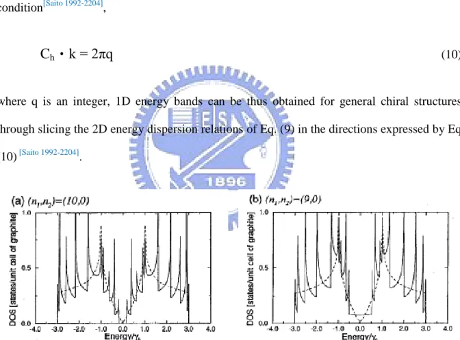
(10)where q is an integer, 1D energy bands can be thus obtained for general chiral structures
through slicing the 2D energy dispersion relations of Eq. (9) in the directions expressed by Eq.
(10) [Saito 1992-2204].
Fig. 2-4 Electronic density of states for two (n, m) zigzag nanotubes: (a) (9, 0) and (b) (10, 0)
[Saito 1992-2204]
As shown in Fig. 2.4, the density of states for two zigzag nanotubes with (n, m) = (10, 0)
and (9, 0) are plotted according to the units of states per unit cell of 2D graphite. For
10
dotted lines. Meanwhile, the l/ singularities of 1D energy bands can be observed at the
band edges of each energy band [Saito 1992-2204]. As shown in Fig. 2.4 (a), it is also observed that
there is an energy gap at the Fermi level, where E = 0, while there is a finite density of states
in Fig. 2.4 (b), and semiconducting (Fig. 2.4(a)) and metallic (Fig. 2.4(b)) nanotube are thus
present. Normally, to determine a nanotube as a metallic type should follow the condition [Saito
1992-2204]
2n + m=3b
(11)where b in an integer. This condition can be obtained by substituting the k vector of the
degenerate point of 2D graphite at the corner of the Brillouin zone into Eq. (10). Normally,
the chiral vectors are only located in the range, – 30o < θ < 0o, as shown in Fig. 2.2 [Saito
1992-2204]
. It is suggested that all armchair nanotubes and zigzag nanotubes should be metallic
when n is a multiple of three [Saito 1992-2204].
Interestingly, it is proposed that if the distribution of Ch vectors shown in Fig. 2.2 is
uniform, l/3 of the nanotubes will be with metallic behaviors and 2/3 of those will be with
semiconducting behaviors [Saito 1992-2204]. However, a larger fraction of metallic CNTs may be
obtained if the initial seed of the tube caps is centered on a pentagon. This leads to an
armchair nanotube [Saito 1992-2204]. On the other hand, if the initial seed is a hexagon other than a
pentagon, the nanotube might be grown with a planar graphite structure [Saito 1992-2204]. Based
on this point, it is suggested that nature might prefer armchair-type nanotubes [Saito 1992-2204].
2.2 Synthetic methods of CNTs
Until recently, many methods have been developed to synthesize CNTs in three primary
approaches including arc-discharge, laser ablation and chemical vapor deposition (CVD) [Lee
2001-245; Pillai 2007-3011]
11
states. Meanwhile, the morphology and properties of CNTs are often controlled with the
process parameters including substrate temperature, precursor gases and gas ratio, catalyst,
pretreatment conditions, and bias voltage, etc. However, the proposed methods still suffer
from the problems, such as low yielding and low uniformities in structure and property.
2.2.1 Arc-discharge method
CNTs were first synthesized by arc-discharge method and identified by Iijima [Iijima 1991-56].
As shown in Figure 2.5 [Saito 1995-979], two graphitic rods are used as anode and cathode in this
arc-discharge system. In the process, arcing occurs when DC voltage is applied between these
two electrodes. With containing small amount of catalysts, such as Fe, Co, Ni, and Y, the
SWCNTs can be synthesized at the anode [Bethune 1993-605] whilst MWNTs can be fabricated
using pure graphite as two electrodes.
Fig. 2-5 Schematic of arc-discharge system[Saito-1995-3062]
The discharge system is normally operated with voltages ranging from 20 to 40 V and
current from 40 to 100 A under He or Ar gas pressure of 10 ~ 500 Torr. Carbon clusters,
collided out from the anodic graphite rod through electron bombardment, are deposited on the
cathode surface. The products on the cathode may include amorphous carbon, fullerenes,
carbon cluster, carbon nanotubes, and other carbon structures. Therefore, post treatment to
12 yielding in producing CNTs.
2.2.2 Laser ablation
Laser ablation was first reported by Guo’s group in 1995 [Guo 1995-49]
, as shown in Fig. 2.6.
An incident laser beam is used to vaporize graphite target under helium or argon gas
atmosphere with pressure of 500 Torr. The products are swept out by the flowing gas and to
be deposited on the water cooled collector. Therefore, it is also named as laser vaporization
method. Normally, the graphite target used in this method often containing Co, Ni, Fe, or Y
and this is a favorable condition of forming SWCNTs.
Fig. 2-6 Schematic of laser ablation system [Guo 1995-49]
2.2.3 Chemical vapor deposition
As shown in Fig. 2.7, thermal chemical vapor deposition[Lee 2001-245] applies the pyrolysis
of hydrocarbon source to synthesize the CNTs. This method is also a catalyst-assisted
SWCNTs growth method and is one of the most commonly used methods. Meanwhile it is
considered the best solution for nanoscale device fabrication because it not only allows a
scalable process but also enables selective growth on patterned catalyst film [Golovko 2005-1636].
The formation of CNTs using CVD involves the formation of small catalyst nanoparticles,
decomposition of hydrocarbon gases such as CH4 and C2H2, and then growth of the nanotubes
13
CVD using hydrogen plasma to form well-distributed and active metallic nanoparticles.
Nanosized catalytically metal particles are formed after the catalytic metal film is etched with
NH3 gas at a temperature ranging from 750 to 1050°C. Reaction gas is supplied from one end
of the apparatus and evacuated from the outlet on the other side. The merit of this method is
capable of depositing large area, and uniform as well as good quality of SWNTs. However the
drawback of this method is not compatible with IC (integrated circuit) process due to the high
working temperature over 600 °C.
Fig. 2-7 Schematic of thermal CVD system [Lee 2001-245]
PECVD system is the most employed method for depositing CNTs [Qin 1998-3437]compared
with the other methods because this method can be compatible to IC process for its low
process temperature and a cheap, less contamination, and high yielding process. Meanwhile,
this process is highly capable of producing controlled alignment of SWCNTs. Therefore,
many new techniques have been developed to prepare vertically aligned SWCNTs through
using this method.
In practical uses, the plasma is activated by a microwave plasma apparatus using RF or
DC discharged system, microwave plasma assisted hot filament, and electron cyclotron
resonance (ECR) plasma source. In general, the typical power supplies used in this method
14
process, SWCNTs are produced by the decomposition of hydrocarbon (such as CH4, C2H2,
C2H4 and C6H6) or monoxide, and then deposition on nanoparticles of transition-metal.
Fig. 2-8 Schematic of MPCVD apparatus [Qin 1998-3437]
Fig. 2-9 Schematic of PE-HF-CVD apparatus[Kurt 2001-1723]
As shown in Fig. 2.8, with the high density of plasma, the MP-CVD system [Qin 1998-3437]
is a contamination-free process and the plasma shape can be regulated through adjusting the
cavity. The PE-HF-CVD system applies the current of the tungsten filament to efficiently
increase the temperature in the process chamber[Kurt 2001-1723] as depicted in Fig. 2.9. As shown
in Fig. 2.10, ECR-CVD system is well known for its advantages of high dissociation
15 of CNTs deposition [Tsai 2001-NCTU].
2.3 The proposed growth mechanisms of catalyst-assisted CVD
In order to well control the synthesizing process of CNTs, it is very important to
understand of the growth mechanism of CNTs. Until recently, although many detailed and
precise growth have been proposed, most of them are still in controversy [Kuo 2004-p9-2].
However, it is believed that the application of catalyst is required to synthesize CNTs in
diameter ranging from 0.7 to 2 nm for the growth process [Kuo 2004-p9-9]. It is also known that
the application of alloy catalyst can increase the growth quantity of SWCNTs significantly.
Some of the growth mechanisms of SWCNTs are demonstrated as blew:
(a) Root growth model
Proposed by Saito et al., this model is used to explain the growth mechanism of radiate
sea-urchin-like SWCNTs by using arc-discharge [Saito 1994-L526]. In their study, numerous
SWCNTs grow from single catalyst particles and their resulting diameters are much smaller
than the particles. It is proposed that carbon-metal alloy can be formed by vaporization during
arc discharge process; this alloy posses higher carbon solubility than in a solid state.
Therefore, the liquid alloy particles tend to segregate excess carbon on their surface with the
decrease of temperature of the cathode.
Two possible occasions can be observed in process. The first is that the cooling rate of
the particles proceeds with a moderate rate and the supersaturated carbon in metal particles is
not high so that carbon is gradually segregated on the particle surface, forming graphitic layer.
Alternatively, the cooling rate is so rapid that the dissolved carbon in a particle is very
16
surface. A large number of tiny flakes are thus forming and subsequently closing their open
ends in order to saturate dangling bonds at their periphery. SWCNTs can then be formed on
the random graphitic flake assembly.
(b) Ball-and-stick catalyst scooting model
This model can be used to explain the phenomenon when catalyst is not found at the tip
of SWCNTs [Birkett 1997-111]. According to the proposal, transition metals show a high propensity
for decoration fullerene surfaces. A carbon fragments bind to the metal clad fullerene and they
may self-assemble as a surrounding circular hexagonal chicken-wire-like fence. Once they are
formed as a belt, the network could propagate as a cylinder. This is so called open edge
growth.
Another similar model, scooter mechanism, considers that a few metal atoms are
chemisorbed and scooted around the open edge of the sheet; and this keeps the tube open and
grows. SWCNT will stop when the metal atoms aggregate and lose their kinetic energy for
scooting.
(c) Vapor-liquid-solid growth mechanism
According to this proposed model [Gorbunov 2002-113], a molten catalyst nanoparticle
penetrates an amorphous carbon aggregate dissolving it and precipitating carbon atom. These
atoms arrange in a graphene sheet whose orientation parallel to the supersaturated
metal-carbon melt is not energetically favorable. Any local defect of this graphene sheet will
result in its buckling and formation of a SWCNT nucleus. Further precipitating carbons
incorporate in edges of growing nanotube, which are anchored to the catalyst nanoparticle by
17
(d) Yarmulke mechanism
Proposed by Dai et al. [Dai 1996-471], this model explains the growth mechanism of CNTs
synthesizing on molybdenum nanoparticles by the disproportionate of CO at 1200 ℃ and
concludes that catalyst size determines the tube diameter. It is also proposed that tubes are
close end and carbon atoms are chemisorbed on the catalyst to for yarmulke first.
Subsequently, carbon source decomposes and defuses into catalyst, making SWCNTs longer.
2.4 The proposed surface modification processes of CNTs
Owing to many unique fascinating properties, many recent studies are devoted to employ
CNTs for various novel applications such as biosensors, drug and vaccine delivery vehicles,
protein transporters, artificial muscles, novel biomaterials, and solar power [Venkatesan 2005- 7154,
Bianco 2005-674, Smart 2006-1034, Chiu 2008-3024, Landi 2005-165]
. Because most applications of CNTs involve
their dispersion in polymer or aqueous matrices, some existing challenges of CNTs can hinder
their success. These challenges result from the presence of an amorphous layer on nanotube
surface, the nonreactive nature of the CNT surface, the nature of agglomeration of CNTs into
bundles, and almost insolubility in any solvent [Felten 2005-074308; Fu 2003-351]. This can significantly
reduce their usefulness [Fu 2003-351, Liu 1998-1253]. To overcome this issue, a modification of the
CNTs by changing their surface chemical composition has proven to be efficient. Meanwhile,
oxygen functionalization can also serve as a purification method for the carbon nanotubes [Lian
2004-8848]
. Furthermore, functionalizing the CNTs with a number of functional groups is known
for increasing their chemical reactivity and can be used as a starting point for further chemical
modification [Boul 1999-367]for some specific applications.
To date, many functionalization methods, such as electrochemical functionalization [Bahr
2001-6542]
18
functionalization [Cao 2002-8971, Ago 1999-8116] and plasma treatment, have been developed to
improve the solubility and to achieve dispersion of CNTs in water or polymers. Among these
techniques, chemical functionalization can be the most common and important way for
surface modification of CNTs [Fu 2003-351].
2.4.1 Chemical processes
The theory behind modification processes is that the formation of polar functional groups
on the surface of CNTs enhances their solubility and dispersion abilities in water or polymers.
At present, the chemical method [Fu 2003-351] is the most common; in this process, CNTs are
normally refluxed or sonicated in a strong acid, such as HNO3 and/or H2SO4, to produce free
radical bonds in sp2 structure on nanotube surface and introduce oxygen containing functional groups, such as carboxylic acids (-COOH), carbonyls (-C=O), and hydroxyls (-OH), to the
radical bonds [Dumitrescu 2007-12944]. However, the harsh conditions inherent in this method may
introduce wall damage, decreasing their stability and even cleaving them into shorter pieces
[Harutyunyan 2002-8671, Zhang 2004-149, Dumitrescu 2007-12944]
. These processes may also give rise to some
unfavorable issues such as waste treatment, as well as time and cost efficiency issues.
Treating nanotubes in mild acid may be an alternative to avoid these issues but this results in a
very low production efficiency.
2.4.2 Plasma processes
Compared with the chemical processes, plasma treatment has gained lots of attention
recently since it is a solvent-free, time efficient, versatile, and environmentally friendly
procedure for surface modification [Wu 2007-1336, Khare 2005-23466, Hassanien 2005-278, Zheng 2007-1622]. In
addition, this method can provide the greatest opportunity to scale up the production if the
19
and etching processes in many industrial fields. To date, many approaches have been
investigated to demonstrate the viability and performance of plasma treatment for surface
modification of CNTs. Among these studies, various gases, such as N2 [Yu 2004-380], H2 [Zhang
2004-54]
, O2[Felten 2005-074308, Ionescu 2006-36, Juan 2005-8231], NH3 [Zheng 2007-1622, Felten 2005-074308, Ionescu 2006-36],
and CF4[Felten 2005-074308, Khare 2004-8166] have been used. Generally, the plasma is generated using
glow discharge, radio frequency discharge, or microwave discharge at low-vacuum pressure.
The generated ions, radicals, and UV light in plasma interact with the CNT surface, creating
free radical bonds on nanotube surface and bonding functional groups to the radical bonds
[Felten 2005-074308]
. Although plasma treatment has been shown to be effective in facial
modification of CNTs, some have mentioned that it may cause serious structural damage due
to the high energy and temperature plasma within very short time [Felten 2005-074308, Xu 2007-8945].
An alternative that circumvents these issues is placing the nanotubes away from plasma
sheath and extracting plasma ions by applying a bias voltage so as to reduce temperature,
radiation, and ion density. However, in most designs, plasma sources are working at around
0.1 to 1 Torr pressure which leads to low mean-free-path; this in turn leads to low etching
efficiency if the alternative is applied. Active plasma at higher-vacuum pressure may be an
optimal solution but this results in a low density plasma that cannot be activated. Therefore, to
seek an optimal method with generating high density plasma in high-vacuum is very
important.
2.5 The characterization methods
2.5.1 Scanning electron microscopy (SEM)
As shown in Fig. 2-10, after Knoll developed the first Scanning electron microscope
(SEM) [Newbury 2000-323], demonstrating most of the basic principles of operation, and a
20
[Newbury 2000-323]
, the SEM has been the most versatile and widely used electron bean instrument
in material characterizations [Joy 1997-465] for their abilities to produce high resolution and
magnification images. In the research filed of CNTs, SEM has traditionally been an important
technique for the characterization of CNTs to monitor the bulk-scale production of CNTs by a
variety of synthetic techniques. It is also the most popular tool to evaluate the quality of
as-grown CNT soot [Itkis 2005-3439].
Fig. 2-10 SEM purity grading system [Itkis 2005-3439]
On the other hand, some drawbacks can be brought while SEM is used to generate high
quality image to evaluate the quality of CNTs [Itkis 2005-3439]. It is mentioned that the metal
catalyst contained in nanotube and a thin coating of amorphous carbon on CNTs are invisible
21
[Itkis 2005-3439]
. Meanwhile, limited by observation scale, more frames with various
magnifications is necessary to provide reliable characterization information [Itkis 2005-3439].
2.5.2 Transmission electron microscopy (TEM)
3
Fig. 2-11 TEM images of (a) SWNTs (b) SWNT bundles (c) DWNT (d) MWNT [Flahaut 2000-249] TEM technique can reveal the interior microstructure of the specimen, and produce the
high-resolution lattice image and the electron diffraction pattern as well. However, in practical
use, some drawbacks can be happened. When TEM is used to directly analyze the structure of
SWCNT, it is difficult to obtain a clear image of one SWCNT. The main reasons are the
structure of SWCNT is easily destroyed by high energy electron beam and electron scattering
are not apparent because of SWCNT is composed of so few carbon atoms. Furthermore,
SWNT is hard to be built on stilts to avoid the background interference from copper grid and
SWNTs dispersion is also an important problem. Figure 2-11 shows the HRTEM images of (a)
SWNTs (b) SWNT bundles (c) DWNT (d) MWNT [Flahaut 2000-249]. A thin layer of amorphous
carbon on nanotube surface may be observed by TEM. However, it is difficult to predict the
precise quantity of the layer amount because the TEM energy is so high that the layer
22
same as SEM technique, with the observation limitation, more frames with various
magnifications is often required to provide homogeneous characterization information.
2.5.3 X-ray photoelectron spectrometry (XPS)
Fig. 2-12 XPS survey spectrum of CNT treated by oxygen plasma [Felten 2005-074308]
Fig. 2-13 XPS C1s spectra of the as-purchased MWCNTs and the five chemical species: (1)
graphite; (2) sp3 carbons; (3) hydroxyl groups; (4) carbonyl groups; and (5) carboxyl groups
[Felten 2005-074308]
XPS has its origins in investigations of photoelectric effect in which X-ray is used as the
exciting source [Briggs 1996-p7]. Based on the equation as below, XPS spectra are obtained by
23
energy (Ek) and number of electrons that escape from the surface of material being analyzed.
E
k=h
v-E
B (12)where hv is the incident photo energy, and EB is the electron binding energy. The heart of this
technique is the measurement of an electron energy spectrum by using an electron energy
analyzer, also called a spectrometer. It is often used to estimate that all aromatic sites at the
surface of the oxidized nanotubes [Felten 2005-074308, Ago 1999-8116, Xu 2007-8945, Ionescu 2006-36, Zhang
2007-2366, Wiltner 2004-881]
. This technique can also be used to identify chemical composition on
material surface and functional groups attached to CNTs. According to the research of Felten
et al. [Felten 2005-074308], MWCNTs are modified by inductive coupled rf-plasma with applying O2,
CF4 and NH3 gases and then investigated by XPS to analysis and quantify the chemical
composition on nanotube surfaces so as to support their experimental results. Figures 2-12
and 2-13 give their XPS investigation results of the oxygen plasma-treated nanotubes. The
XPS survey spectrum in Fig. 2-12 is used to confirm the chemical elements on the surface of
nanotubes. The XPS C1s spectrum in Fig. 2-13 is deconvoluted into five Gaussian peaks
centered at 284.5, 285.1, 286.2, 287.2, and 288.9 eV after the background are subtracted. The
main peak at 284.5 eV originates from the graphite signal. The peak at 285.1 eV is attributed
to sp3 carbon atoms. The peaks at 286.2, 287.2, and 288.9 eV correspond to hydroxyl, carbonyl (or ether), and carboxyl (or ester) groups respectively. The XPS results show that
after thee nanotubes are treated by the oxygen plasma under various process conditions, the
[O]/[C] ratio which is the relative percentage of the oxidized carbon species to total number of
24
2.5.4 Raman spectroscopy
Raman spectroscopy provides information about molecular vibrations that can be used
for sample identification and quantification. Normally, a monochromatic light (laser) incident
on a sample, the photons which make up the light may be absorbed or scattered, or may not
interact the material and may pass through it. When light is scattered from an atom or
molecule, most photons are elastically scattered (Rayleigh scattering), such that the scattered
photons have almost the same frequency as the incident photons. However, a small fraction of
the scattered light (approximately 1 in 106-108
photons) is scattered by an excitation, with
the scattered photons having a frequency different from, and usually lower than, the frequency
of the incident photons [Smith 2005-p2]. The energy difference between the monochromatic light
and the Raman scattered light is equal to the energy involved in changing the molecule’s
vibration state [Smith 2005-p2]. This energy difference is then called the Raman shift [Smith 2005-p2].
Several different Raman shifted signals will often be observed; each being associated with
different vibrational or rotational motions of molecules in the sample. Figure 2-14 shows the
schematic diagram of state change of Raman scattering [Rao 1997-187]. In CNTs research field,
the Raman scattering from SWCNTs is resonantly enhanced if the excitation energy (EL)
matches the separations between the pairs of Van Hove singularities (Eii) in the
one-dimensional electronic density of states of the SWCNTs, as shown in Fig. 2-4 [Itkis 2005-3439]
and Fig. 2-15. It is widely used as a sensitive prober to analysis the electronic structure in
25
Fig. 2-14 Schematic of state change of Raman scattering [Rao 1997-187]
Fig. 2-15 The left panel shows the electronic transition energies Eii vs. nanotube diameter dt. The right panels show schematic figures defining the SWNT classes: MOD0 — metallic, where one cutting line crosses the K point; MOD1 and MOD2 — semiconducting [Dresselhaus 2005-47]
In the inspection of carbon nanostructures, there are two characteristic peaks in Raman
spectrum represented as D and G bands. The D mode at around 1300 cm−1 is correlated with structural disorder of CNTs, which originates from the defects including disordered materials,
poor graphitization, functionalized carbon, and the amorphous carbon on the sidewall of
nanotubes [Shaijumon 2007-75, Dillon 2004-691, Jian 2008-230]. The relative intensity of this mode can
provide direct evidence of covalent modification and defect concentration. When estimating
the defect concentration, the D mode intensity is usually normalized with respect to the
26
intensity of the G mode is independent of defect concentration and originates from a single
resonant Raman process [Jian 2008-230]. On the other hand, if the G mode is induced by defects,
this procedure for normalizing the intensity is no longer correct [Maultzsch 2002-2647].
The radial breathing mode (RBM) can be used to study nanotube diameter through its
frequency (
ω
RBM) and to perform (n, m) assignment of SWCNTs by analyzing both dt andIRBM [Dresselhaus 2005-47]. As shown in Fig. 2-16, the RBM of Raman spectrum is a unique feature
to SWNTs and involves a collective vibrational movement of the carbon atoms towards and
away from the central axis of a SWCNT. It occurs with
ω
RBM ranging from 120 to 350 cm-1for diameters, dt, ranging from 0.7 nm to 2 nm [Dresselhaus 2005-47]. It is therefore very useful for
indentifying if a given carbon materials contains SWCNTs.
Fig. 2-16 Raman spectra from a metallic (top) and a semiconducting (bottom) SWNT at the single nanotube [Dresselhaus 2005-47]
RBM frequency for nanotube diameter
The RBM oscillations strongly correlate with a periodicity imposed on a graphene sheet
by wrapping it into a finite-size nanotube with small diameter. Consequently, the associated
RBM wavelength and frequency are directly related to the perimeter of the nanotube [Dresselhaus
2005-47]
, as shown in Fig. 2-17. Based on this relationship, as the diameter of the nanotube
27
nanotubes and MWCNTs the RBM frequency becomes very small and, at the same time, the
intensity of the RBM decreases and ultimately becomes undetectable by Raman spectroscopy
measurements. Hence Dresselhaus et al. [Dresselhaus 2002-2043]proposed that the frequency of the
RBM are: B d A t RBM (13)
where A = 234 or 248 cm-1 nm and B = 10 or 0 cm-1 for bundle or isolated SWCNTs on silicon wafer, respectively [Dresselhaus 2005-47]. Note that, for larger diameter tubes (dt > 2 nm), the
intensity of the RBM is very weak and hardly detected. Meanwhile, it should be noted that a
single Raman measurement can give an idea of the nanotubes that are resonance with the laser
line. However, this cannot give a complete characterization of the diameter distribution of the
sample. Alternatively, using many laser lines with different excitation energies can obtain a
good characterization of the diameter distribution in the sample.
Fig. 2-17 The Raman vibration modes of CNTs (a) G-band mode (b) D-band mode (c) Radial breath mode [Raravikar 2002-235424]

![Fig. 2-5 Schematic of arc-discharge system [Saito-1995-3062]](https://thumb-ap.123doks.com/thumbv2/9libinfo/8625088.191835/26.892.119.813.485.856/fig-schematic-of-arc-discharge-system-saito.webp)
![Fig. 2-7 Schematic of thermal CVD system [Lee 2001-245]](https://thumb-ap.123doks.com/thumbv2/9libinfo/8625088.191835/28.892.248.775.412.755/fig-schematic-thermal-cvd-lee.webp)
![Fig. 2-9 Schematic of PE-HF-CVD apparatus [Kurt 2001-1723]](https://thumb-ap.123doks.com/thumbv2/9libinfo/8625088.191835/29.892.293.659.222.848/fig-schematic-pe-hf-cvd-apparatus-kurt.webp)
![Fig. 2-12 XPS survey spectrum of CNT treated by oxygen plasma [Felten 2005-074308]](https://thumb-ap.123doks.com/thumbv2/9libinfo/8625088.191835/37.892.176.760.273.887/fig-xps-survey-spectrum-treated-oxygen-plasma-felten.webp)
![Fig. 2-14 Schematic of state change of Raman scattering [Rao 1997-187]](https://thumb-ap.123doks.com/thumbv2/9libinfo/8625088.191835/40.892.300.641.112.394/fig-schematic-state-change-raman-scattering-rao.webp)
![Fig. 2-16 Raman spectra from a metallic (top) and a semiconducting (bottom) SWNT at the single nanotube [Dresselhaus 2005-47]](https://thumb-ap.123doks.com/thumbv2/9libinfo/8625088.191835/41.892.320.643.501.804/raman-spectra-metallic-semiconducting-swnt-single-nanotube-dresselhaus.webp)
![Fig. 2-17 The Raman vibration modes of CNTs (a) G-band mode (b) D-band mode (c) Radial breath mode [Raravikar 2002-235424]](https://thumb-ap.123doks.com/thumbv2/9libinfo/8625088.191835/42.892.123.807.500.930/fig-raman-vibration-modes-cnts-radial-breath-raravikar.webp)
![Fig. 2-19 The weight loss (solid) and weight derivative (dash) curves of TGA [Harutyunyan 2002-8671]](https://thumb-ap.123doks.com/thumbv2/9libinfo/8625088.191835/45.892.148.790.381.749/fig-weight-loss-solid-weight-derivative-curves-harutyunyan.webp)
