IEEE ELECTRON DEVICE LETTERS, VOL. 34, NO. 4, APRIL 2013 511
Low Temperature Improvement Method on Zn:SiO
x
Resistive Random Access Memory Devices
Kuan-Chang Chang, Tsung-Ming Tsai, Ting-Chang Chang, Senior Member, IEEE, Hsing-Hua Wu, Kai-Huang
Chen, Jung-Hui Chen, Tai-Fa Young, Tian-Jian Chu, Jian-Yu Chen, Chih-Hung Pan, Yu-Ting Su, Yong-En Syu,
Cheng-Wei Tung, Geng-Wei Chang, Min-Chen Chen, Hui-Chun Huang, Ya-Hsiang Tai, Der-Shin Gan,
Jia-Jie Wu, Ying Hu, and Simon M. Sze, Life Fellow, IEEE
Abstract— To improve the resistive switching properties of the resistive random access memory (RRAM), the supercritical carbon dioxide (SCCO2) fluid is used as a low temperature treat-ment. In this letter, the Zn:SiOxthin films are treated by SCCO2 fluid mixed with pure water. After SCCO2 fluid treatment, the resistive switching qualities of the Zn:SiOxthin films are carried
out by XPS, fourier transform infrared spectroscopy, and IV measurement. We believe that the SCCO2-treated Zn:SiOx thin
film is a promising material for RRAM applications due to its compatibility with portable flat panel display.
Index Terms— Nonvolatile memory, resistive switching, silicon oxide, zinc.
I. INTRODUCTION
R
ECENTLY, the nonvolatile resistance random access memory (RRAM) has been widely discussed and inves-tigated for applications in various memory devices because of its excellent memory characteristics, high storage capacity, long retention cycles, low operation voltage, and low electric consumption [1]–[6]. In addition, the various materials have Manuscript received November 28, 2012; accepted February 9, 2013. Date of publication March 13, 2013; date of current version March 20, 2013. This work was supported the National Science Council Core Facilities Laboratory for Nano-Science and Nano-Technology in the Kaohsiung-Pingtung area and the National Science Council of the Republic of China under Contract NSC-101-2120-M-110-002 and Contract NSC 101-2221-E-110-044-MY3. The review of this letter was arranged by Editor D. Ha.K.-C. Chang, T.-M. Tsai, T.-J. Chu, C.-H. Pan, C.-W. Tung, H.-C. Huang, and D.-S. Gan are with the Department of Materials and Optoelectronic Science, National Sun Yat-Sen University, Kaohsiung 804, Taiwan.
T.-C. Chang, J.-Y. Chen, Y.-T. Su, Y.-E. Syu, and M.-C. Chen are with the Department of Physics, National Sun Yat-Sen University, Kaohsiung 804, Taiwan. They are also with the Advanced Optoelectronics Tech-nology Center, National Cheng Kung University, 70101, Taiwan (e-mail: [email protected]).
H.-H. Wu, G.-W. Chang, and Y.-H. Tai are with the Department of Photonics and the Institute of Electro-Optical Engineering, National Chiao Tung University, Hsinchu 30050, Taiwan.
K.-H. Chen is with the Department of Electronics Engineering and Com-puter Science, Tung-Fang Design University, Kaohsiung 807, Taiwan.
J.-H. Chen is with the Department of Chemistry, National Kaohsiung Normal University, Kaohsiung 80543, Taiwan.
T.-F. Young is with the Department of Mechanical and Electro-Mechanical Engineering, National Sun Yat-Sen University, Kaohsiung 804, Taiwan.
J.-J. Wu and Y. Hu are with the School of Technical Physics, Xidian University, Xi’an 710071, China.
S. M. Sze is with the Department of Physics, National Sun Yat-Sen Uni-versity, Kaohsiung 804, Taiwan, and also with the Department of Electronics Engineering, National Chiao Tung University, Hsinchu 30050, Taiwan.
Color versions of one or more of the figures in this letter are available online at http://ieeexplore.ieee.org.
Digital Object Identifier 10.1109/LED.2013.2248075
been reported to possess resistive switching behaviors, silicon-based oxide is a promising material for RRAM applica-tions because of its great compatibility in integrated circuit processes. Therefore, the research using silicon-based oxide as the resistance-switching layer was worthy of investigation. Lately, the liquid-like and excellent properties of the supercrit-ical carbon dioxide (SCCO2) fluid have attracted considerable research in efficiently transporting H2O molecules and no damaging diffusion into the microstructures of dielectric layer at a low-temperature treatment. Decreased and passivated the traps and defects of thin films have their advantages [7]–[11]. In this letter, zinc metal doped into SiO2 by co-sputtering at room temperature was taken as the resistance switching layer of RRAM. To demonstrate the resistive switching mechanism of zinc-doped SiO2(Zn:SiOx) layer dominated by interface of TiN electrode or Zn:SiOx film, the Pt/Zn:SiOx/TiN device was fabricated in virtue of inertia of Pt electrode as top electrode. In addition, the material and conduction mechanism analyses were discussed to explain the effect of the SCCO2 fluid on Zn:SiOx resistive switching behaviors.
II. EXPERIMENTALSETUP
The experimental samples were divided into two steps to verify the feasibility of SCCO2 to improve the resistive switching properties of Zn:SiOx RRAM. First, the Zn:SiOx thin film (about 30 nm) was deposited on the TiN/Ti/SiO2/Si substrate by co-sputtering with the pure SiO2 and zinc tar-gets. Sequentially, the Zn:SiOx thin films were placed in a supercritical fluid system with 165-ml chamber size at 150 ◦C for one hour, it was injected with 3000 psi SCCO2 fluids, which were mixed with 0.5-ml pure H2O. Therefore, the water will be solved into SCCO2 fluids with a mole concentration of 0.17 M in the reactive chamber. Finally, the Pt top electrode of 200-nm thickness was deposited on Zn:SiOx film to form Pt/Zn:SiOx/TiN sandwich structure. The entire electrical measurements of devices with the Pt electrode of 250-μm diameter were performed using Agilent B1500 semiconductor parameter analyzer.
III. RESULTS ANDDISCUSSION
To analyze and discuss the influence of Zn element on resistance switching characteristics in SiO2 thin film, the chemical bonding of the Zn:SiOx film was investigated by the 0741-3106/$31.00 © 2013 IEEE
512 IEEE ELECTRON DEVICE LETTERS, VOL. 34, NO. 4, APRIL 2013
(a)
(b)
(c)
Fig. 1. (a) FTIR spectrums of Zn:SiOx film with (red line) and without
(blue line) SCCO2 treatment. (b) Enlargement of Si-O-Zn stretch bonding for SCCO2-treated and untreated Zn:SiOx. (c) Enlargement of the Si-O-Si
bending mode bonds for SCCO2-treated and untreated Zn:SiOx.
Fourier transform infrared spectroscopy (FTIR) in this letter. Fig. 1 shows the Si-O-Zn stretch bonding was found in the Zn:SiOx film at 1080 cm−1 from the FTIR spectrums. In addition, the anti-symmetric stretch mode and the symmetric stretch mode of Si-O-Si bonds were discovered at 1040 and 835 cm−1, respectively. In addition, the peaks at 1080 cm−1 belonged to the Si-O-Zn stretch bonding and the peak at 1040 cm−1 belonged to the bending mode of Si-O-Si bonds were shown in Fig. 1(a) and (b). According to these absorption peaks expressed in FTIR spectrums, we can confirm the Zn element was bonded with oxygen element in the SiO2 film. According to Beer’s law, the Si-O-Zn stretch bonding intensity of the SCCO2-treated thin films was improved from 0.018 to 0.02 shown in insert of Fig. 1(b). Besides, the Si-O-Si stretch bonding intensity of the SCCO2 treated thin films was improved from 0.0247 to 0.0251 shown in Fig. 1(c). However, the intensity of O-H stretch bonding for SCCO2 -treated Zn:SiOx film was decreased. This result indicated that the oxygen and silicon atoms for the SCCO2-treated Zn:SiOx film were combined and integrated and the Si-O-Si binding of thin films was closer and denser.
To analyze the influence of SCCO2 treatment on chemical composition characteristics in Zn:SiOx thin film, the mole fraction of Zn:Si:O in the co-sputtered Zn:SiOx film was 4.9%:24.9%:70.2% by calculated from the peak areas of Zn, Si, and O XPS spectra. We also found that the Zn:Si:O in the SCCO2-treated Zn:SiOx thin film was 3.8%:23.4%:72.08%. The intensity of Zn-O binding energy in Zn:SiOx thin film was increased from 45.13 to 64.7% based on the deconvolution signal from the Zn 2P3/2 core level XPS spectra in Zn:SiOx film after SCCO2 treatment. In addition, the mole fraction of oxygen in Zn:SiOx film was also increased from 70.2 to 72.08% after SCCO2 treatment. This result indicated that operation current and resistance state of Zn:SiOx thin film were improved by SCCO2 treatment process because of its oxidation and repaired damage ability.
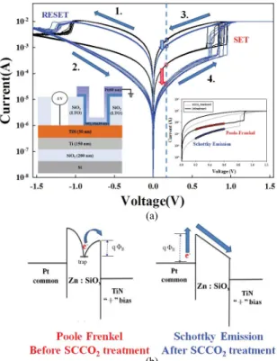
In order to further discuss the resistance switching mech-anisms in the co-sputtered and SCCO2-treated Zn:SiOx thin film, the high resistive state (HRS) and the low resistive state
(a)
(b)
Fig. 2. (a) Current–voltage curves are the resistive switching characteristics of Zn:SiOxdevice with and without SCCO2treatment. The current conduction in HRS for Zn:SiOxdevice is transferred from Poole–Frenkel conduction to
Schottky emission after SCCO2 treatment. (b) Band diagrams of Zn:SiOx
RRAM device before and after SCCO2treatment.
(LRS) of current–voltage (I–V) curves were discussed and investigated for the current conduction mechanisms. Fig. 2(a) shows typical I–V characteristics of the Zn:SiOx RRAM devices with and without SCCO2 treatment, which exhibit the bipolar behavior by applying bias on TiN electrode as shown in inset of Fig. 2(a) (left), and the current compliance was set at 10 mA to prevent the permanent breakdown of devices during operation. By sweeping the bias to negative over the reset voltage, a gradual decrease of current was presented to switch the cells from LRS to HRS (reset process). Conversely, the cell turns back to LRS while applying a larger positive bias than the set voltage (set process).
As shown in Fig. 2(a), the HRS state of the Zn:SiOx thin films treated by SCCO2 was also decreased from 0.2 to 0.02 mA. The HRS state of the SCCO2-treated films was ten times lower than untreated films. In applied voltage of 0.21∼0.58 V, the untreated thin films for HRS state were the Poole–Frankel emission conduction by ln(I/V)-V1/2 curve fitting. According to experimental results, we suggested that doping zinc into SiO2 resulted in an increased amount of hetero-defects in the Zn:SiOx thin films. For this reason, the electrons were transferred through the hetero-defects to make the current conduction dominated by Poole–Frenkel conduction. In addition, the SCCO2-treated films for HRS state obey the Schottky Emission conduction in lnI-V1/2curve. The transfer of Poole–Frenkel to Schottky Emission conduc-tion was attributed to defect and oxygen vacancy decreased and repaired in bulk Zn:SiOx thin films after SCCO2treatment [Fig. 2(b)].
CHANG et al.: LOW TEMPERATURE IMPROVEMENT METHOD ON Zn:SiOxRRAM DEVICES 513
(a)
(b)
(c)
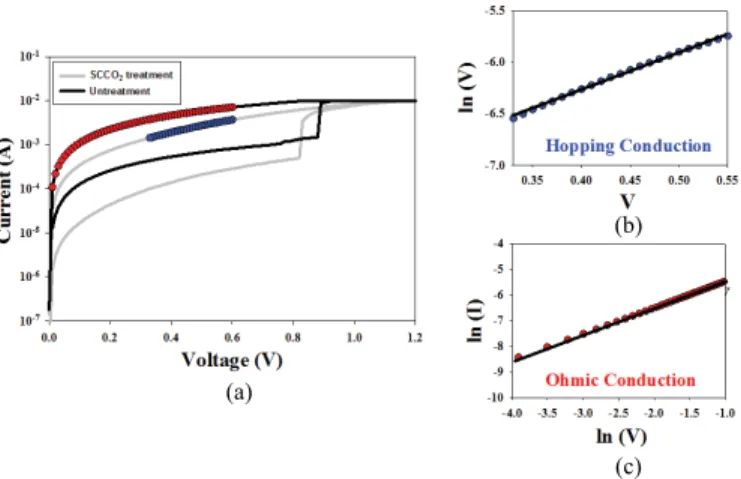
Fig. 3. (a) Electrical characteristics of Zn:SiOxdevice with (blue cycle) and
without (red cycle) SCCO2 treatment. (b) A plot of ln(I) versus V in low resistance state (LRS) for SCCO2-treated Zn:SiOxdevice. (c) A plot of ln(I)
versus ln(V) in LRS for untreated Zn:SiOxdevice.
As shown in Fig. 3, the LRS state of the Zn:SiOx thin films prepared by SCCO2 treatment was decreased from 2 to 0.8 mA at a reading voltage of 0.1 V. The LRS state of the SCCO2-treated films was twice lower than untreated films. The untreated thin films exhibited the ohmic conduction by ln(I)-ln(V) curve fitting. This result indicated that the conductive filament formed by the current flowing through the zinc-induced defect in the Zn:SiOx film. In addition, the SCCO2 -treated thin films exhibited the hopping conduction by ln(I)-V curve fitting. According to the relationship of hopping con-duction, J = q Naυ0e−q Ea/K TeqaV/2dkT, where N, a, υ0, Ea, and d are density of space charge, mean of hopping distance, intrinsic vibration frequency, barrier height of hopping, and film thickness, respectively. The hopping conduction is due to trapped electrons surpass to the Ea barrier and form the leakage current for the SCCO2-treated device. We found and suggested the active energy barrier lowering of SCCO2-treated thin films caused by trapped electrons jump from the defects and form continuous potential well with positive charges [12]. The change of carrier transport in Zn:SiOx will reduce power consumption and joule heating degradation of RRAM due to hydration–dehydration reaction through SCCO2 treatment at low temperature.
IV. CONCLUSION
In conclusion, the bipolar resistance switching character-istics were successfully achieved by doping Zn metal into SiO2 film for untreated and treated SCCO2 fluid treatment. To analyze HRS state of current fitting, the conduction mech-anism of thin films for untreated and treated SCCO2 process obeys the Poole–Frankel model and Schottky Emission model, respectively. For LRS state of current fitting, the untreated and treated thin films exhibited the ohmic contact model and
hopping conduction model, respectively. Besides, we believed that the resistance switching performance of silicon oxide-based RRAM device can be improved in virtue of SCCO2low temperature treatment for IC applications. Finally, the smaller operated current and lower power consumption of the Zn:SiOx thin films can be effectively achieved by SCCO2treatment at low temperature for portable flat panel display applications.
REFERENCES
[1] T. M. Tsai, K. C. Chang, T. C. Chang, Y.-E. Syu, S.-L. Chuang, G.-W. Chang, G.-R. Liu, M.-C. Chen, H.-C. Huang, S.-K. Liu, Y.-H. Tai, D.-S. Gan, Y.-L. Yang, T.-F. Young, B.-H. Tseng, K.-H. Chen, M.-J. Tsai, C. Ye, H. Wang, and S. M. Sze, “Bipolar resistive RAM characteristics induced by nickel incorporated into silicon oxide dielectrics for IC applications,” IEEE Electron Device Lett., vol. 33, no. 12, pp. 1696–1698, Dec. 2012.
[2] Y. E. Syu, T. C. Chang, T. M. Tsai, Y. C. Hung, K. C. Chang, M. J. Tsai, M. J. Kao, and S. M. Sze, “Redox reaction switching mechanism in RRAM device with Pt/CoSiOX/TiN structure,” IEEE Electron Device Lett., vol. 32, no. 4, pp. 545–547, Apr. 2011.
[3] K. C. Chang, T. M. Tsai, T. C. Chang, Y. E. Syu, S. L. Chuang, C. H. Li, D. S. Gan, and S. M. Sze, “The effect of silicon oxide based RRAM with tin doping,” Electrochem. Solid-State Lett., vol. 15, no. 3, pp. H65–H68, 2012.
[4] Q. Liu, S. B. Long, W. Wang, Q. Y. Zuo, S. Zhang, J. N. Chen, and M. Liu, “Improvement of resistive switching properties in ZrO2-based ReRAM with implanted Ti ions,” IEEE Electron Device Lett., vol. 30, no. 12, pp. 1335–1337, Dec. 2009.
[5] Y. Wang, Q. Liu, S. B. Long, W. Wang, Q. Wang, M. H. Zhang, S. Zhang, Y. T. Li, Q. Y. Zuo, J. H. Yang, and M. Liu, “Investiga-tion of resistive switching in Cu-doped HfO2 thin film for multilevel non-volatile memory applications,” Nanotechnology, vol. 21, no. 4, p. 045202, 2010.
[6] Y. T. Li, S. B. Long, M. H. Zhang, Q. Liu, L. B. Shao, S. Zhang, Y. Wang, Q. Y. Zuo, and S. Liu, and M. Liu, “Resistive switching properties of Au/ZrO2/Ag structure for low voltage nonvolatile memory applications,” IEEE Electron Device Lett., vol. 31, no. 2, pp. 117–119, Feb. 2010.
[7] C. T. Tsai, T. C. Chang, P. T. Liu, P. Y. Yang, Y. C. Kuo, K. T. Kin, P. L. Chang, and F. S. Huang, “Low-temperature method for enhancing sputter-deposited HfO2 films with complete oxidization,” Appl. Phys.
Lett., vol. 91, no. 1, pp. 012109-1–012109-3, Jul. 2007.
[8] T. M. Tsai, K. C. Chang, T. C. Chang, Y. E. Syu, K. H. Liao, B. H. Tseng, and S. M. Sze, “Dehydroxyl effect of Sn-doped silicon oxide resistance random access memory with supercritical CO2 fluid treatment,” Appl. Phys. Lett., vol. 101, no. 11, pp. 112906-1–112906-4, Sep. 2012.
[9] M. C. Chen, T. C. Chang, S. Y. Huang, K. C. Chang, H. W. Li, S. C. Chen, J. Lu, and Y. Shi, “A low-temperature method for improving the performance of sputter-deposited ZnO thin-film-transistors with supercritical fluid,” Appl. Phys. Lett., vol. 94, no. 16, pp. 162111-1–162111-3, Apr. 2009.
[10] K. C. Chang, T. M. Tsai, T. C. Chang, Y. E. Syu, C.-C. Wang, S. K. Liu, S. L. Chuang, C. H. Li, D. S. Gan, and S. M. Sze, “Reducing operation current of Ni-doped silicon oxide resistance random access memory by supercritical CO2 fluid treatment,” Appl. Phys. Lett., vol. 99, no. 26, pp. 263501-1-263501-4, Dec. 2011.
[11] T. M. Tsai, K. C. Chang, T. C. Chang et al., “Origin of hop-ping conduction in Sn-doped silicon oxide RRAM with supercritical CO2 fluid treatment,” IEEE Electron Device Lett., vol. 33, no. 12, pp. 1693–1695, Dec. 2012.
[12] T. Y. Tseng and H. Nalwa, Handbook of Nanoceramics and Their Nased Nano Devices, Valencia, CA, USA: American Scientific Pub., 2009, pp. 175–176.