Switching Between Transverse Electric and Magnetic Mode in
InAs/AlGaAs/GaAs Quantum Dot Infrared Photodetector
Shen-De Chen, Ying-Ying Chen, and Si-Chen Lee
Department of Electrical Engineering/Graduate Institute of Electronics Engineering
National Taiwan University, Taipei, Taiwan, Republic of China
Abstract — By introducing a 2-nm-Al0.3Ga0.7As capping
layer on the InAs quantum dots, a transverse electric (TE) field dominant response in quantum dot infrared photodetector (QDIP) has been achieved. The TE enhanced peaks are due to the transition from the S-like ground state to the P-like first excited states induced by the strain on the quantum dot. After rapid thermal annealing (RTA), the compressive strain changes. Therefore, the TE favorite peaks can be changed to transverse magnetic (TM) field enhanced and vice versa.
Index Terms — InAs quantum dot, infrared photodetector,
polarization, solid source molecular beam epitaxy, transverse electric field, transverse magnetic field.
I. INTRODUCTION
Compared to the quantum well infrared photodetector (QWIP) or superlattice infrared photodetector (SLIP), the 3D confinement of InAs QDIP can increase the TE response resulting from the intersubband transition [1]. Thus, QDIP has the advantage over QWIP or SLIP when applying in the focal plane array, i.e. normal incident absorption without grating coupling. What the interesting thing is that there is still TE-mode response in the SLIP [1]. In the early years during the development of QWIP, i.e., GaAs/AlGaAs, InGaAs/InAlAs, and InGaAs/AlAs [2-6], many researchers observed the TE absorption as well as the transverse magnetic (TM) absorption and this was attributed to the formation of a strain induced energy level which favors TE absorption. Several different explanations, such as spin-flip intersubband transitions induced by the spin-orbit coupling [9] and the D2d
tetragonal perturbation of the local (crystal and strain) field effects on the quantum well [4], were also proposed in their reports.
In this paper, the polarization-resolved responses of multi-color InAs/AlGaAs/GaAs QDIP are reported. The responses are TE or TM mode enhanced, depending on the detection wavelength and post-growth annealing. Possible mechanisms were also proposed.
II. EXPERIMENTS
The InAs/AlGaAs/GaAs QDIP was grown by a VG V80 solid-source molecular beam epitaxy (MBE) on (100) semi-insulating GaAs substrate. The ten-stacked active region was grown at 510℃. Every stack consisted of 2.2 monolayer (ML) Si-doped InAs QDs covered with 2 nm Al0.3Ga0.7As and 30 nm GaAs spacer. After the growth of
InAs QDs, all shutters were closed for 5 sec to allow atoms to migrate on the surface. The active region was sandwiched by two 15-nm-thick Al0.3Ga0.7As blocking
layers grown at 510℃ in order to block the dark current and n-GaAs contact layers were grown at 580 ℃. The dopant concentrations in both InAs QDs and contact layers are 1×1018cm−3. After growth, the samples were
processed with or without rapid thermal annealing (RTA) at 650 ℃ for 30, 60, and 90 sec as a comparison. Finally, the 100×100
µ
m2 device was fabricated by standardlithography process. The responsivity of the device was measured under an 450-edge-coupling scheme, as shown
as Figure 1, with closed-cycle cryogenics and Perkin-Elmer S2000 Fourier transform infrared spectroscopy.
III. RESULTS AND DISCUSSION
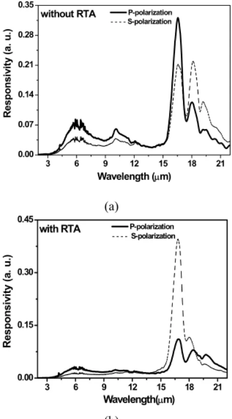
Figure 2 shows the polarization-resolved spectral responses of 2.2 ML InAs/AlGaAs/GaAs QDIPs (a) before and (b) after RTA, respectively. The S and P polarizations of incident light are defined as shown in Fig. 1(b). The S-polarization stands for the TE mode, and the P-polarization has the electric field component parallel to the growth direction. The two shorter-wavelength peaks at 6 and 10 µm are suggested to be due to the bound-to-continuous transitions from InAs QDs with different size distributions, and the responsivities of TM mode are larger than those of TE mode both with and without RTA. This result is in good agreement with the previous reports of conventional InAs/GaAs QDIPs [4, 10-12]. The non-zero responsivity of the TE mode is usually suggested as being resulted from the non-planar shaped dots. Another minor factor is the breaking of symmetry/asymmetry of Proceedings of 2005 5th IEEE Conference on Nanotechnology
Nagoya, Japan, July 2005
wave functions due to the Si dopants in the QDs. As shown in the figure, all the peak positions almost stay the same or just slightly shift while changing the polarizations. This indicates that the anisotropic strain inside QD comes from both the lateral and vertical confinements which mix the wave functions and create a single broad peak whose position is independent of polarization. On the other hand, the energy separations between TE and TM mode absorptions exist both in strained and unstrained quantum wells [4-6]. The three peaks located around 16 µm are assigned to be the ground state to first excited state transitions within QD of different sizes, different trends are observed in terms of different polarizations.
In Fig. 2(a), the 18- and 19.3-µm peaks exhibit unexpected TE-dominant responses while the 16.5-µm peak is still TM-mode favorite. Although Maimon et al [10] have reported almost equal responsivities in both S and P polarizations, the strongly TE dominant responses and their changes with respect to polarizations, to our knowledge, are first observed. Peng et al [4] have shown that, at Brillouin zone center
k
=
0
, the ground state, corresponding tol
=
0
, will be S-like; while the excited states, corresponding tol
=
1
, are P-like triply degenerate states that will split into a(
P
x,
P
y)
doublet,
1
(
m
l=
m
TE active) and aP
z singlet(
m
l=
0
,
TM active) under a tetragonal perturbation. Their work proved that both TE and TM mode absorptions from ground to first excited states are possible and the observed splitting between TE and TM absorption peaks is due to theD
2d tetragonal perturbation of the local (crystal and strain) field effects on the quantum well. For our QDIP, the strain inside the InAs QD is anisotropic [11] which is unlike the in-plane stress in the quantum well. This anisotropic strain couples the doublet and singlet and makes the splitting between(
P
x,
P
y)
doublet andP
z singlet less. Also, the in-plane confinement contributes to the TE mode response. Finally, with the unmissable large fluctuation of dot size, in-plane quantum confinement and anisotropic strain, the non-zero TE mode or S-polarization dominant responses represented in Fig. 2(a) without energy shift could be explained as the contributions from the(
P
x,
P
y)
doublet.Moreover, the responses of the 2.2 ML InAs/AlGaAs/GaAs QDIP changed with respect to electric field polarization after RTA, as shown in Fig. 2(b). Without RTA, the three peaks from short to long wavelength around 18 µm exhibit TM, TE, and TE dominant response, respectively. After RTA, they become TE, TE, and TM dominant, respectively. We have examined several devices with the same structure, this changing behavior is assured. Also, the PL spectra of the same structure with different RTA times, i.e. 30, 60, 90 seconds, are measured as shown in Fig. 3. It is clear from
the figure that the PL peak position red shifted and the intensity decreases while increasing the annealing time from 0 to 90 seconds. It is suggested that the RTA process breaks the bounds and creates defects at the interface of QD and its surrounding material. These defects relax the compressive strain within QDs. Thus, the PL intensity decreases and the peak position red shifted. The current-voltage characteristics, as shown in Fig. 4, reconfirms this explanation. After 30-sec RTA, the dark current slightly increases under the same bias. After 60-sec RTA, the dark current increases rapidly. The curve of the 90-sec RTA is not shown here because it exceeds the maximum of our measurement system. It indicates that the RTA-induced defects form leakage channels, so the dark current increases after RTA.
IV.CONCLUSIONS
In summary, we have successfully fabricated InAs/AlGaAs/GaAs QDIPs with enhanced TE mode response which can be engineered by RTA. Three peaks were observed in the long-wavelength infrared region around 18 μ m. They exhibit different polarization selective responses and can be changed by RTA. It is due to the transition from the S-like ground state to the strain induced splitting of P-like first excited states.
ACKNOWLEDGEMENT
This work is supported by the National Science Council of Republic of China under contact No. NSC 92-2120-M-002-029.
REFERENCES
[1] Shih-Yen Lin, Yao-Jen Tsai, and Si-Chen Lee, Jpn. J.
Appl. Phys. 40, L 1290 (2001).
[2] H. C. Liu, M. Buchanan, and Z. R. Wasilewski, Phys. Rev.
B 44, 1411 (1991).
[3] D. Elbert, E. Ehrenfreund, J. Bajaj, G. J. Sullivan, and D. Lind, J. Appl. Phys. 71, 6199 (1992).
[4] L. H. Peng, J. H. Smet, T. P. E. Broekaert, and C. G. Fonstad, Appl. Phys. Lett. 61, 2078 (1992).
[5] H. S. Li, R. P. G. Karunasiri, Y. W. Chen, and K. L. Wang,
J. Vac. Sci. Technol. B 11, 922 (1993).
[6] Gamani Karunasiri, Jin Suk Park, John Chen, Robert Shih, J. F. Scheihing, and M. A. Dodd, Appl. Phys. Lett. 67, 2600 (1995).
[7] S. Sauvage, P. Boucaud, F. H. Julien, J. M. Gerard, and V. Thierry-Mieg, Appl. Phys. Lett. 71, 2785 (1997).
[8] S. J. Chua, S. J. Xu, X. H. Zhang, X. C. Wang, T. Mei, W. J. Fan, C. H. Wang, J .Jiang, and X. G. Xie, Appl. Phys. Lett. 73, 1997 (1998).
[9] S. Sauvage, P. Boucaud, T. Brunhes, V. Immer, E. Finkman, and J. –M. Gerard, Appl. Phys. Lett. 78, 2327(2001).
[10] S. Maimon, E. Finkman, G. Bahir, S. E. Schacham, J. M. Garcia, and P. M. Petroff, Appl. Phys. Lett. 73, 2003(1998). [11] H. S. Lee, J. Y. Lee, T. W. Kim, and M. D. Kim, Appl Phys.
Lett. 83, 2256 (2003).
Fig. 1. the 450-edge-coupling scheme and the definition of
polarizations.
(a)
(b)
Fig. 2. Spectral response of 2.2 ML InAs/AlGaAs/GaAs QDIP in terms of polarization (a) without and (b) with RTA.
Fig. 3. PL spectra of 2.2 ML InAs/AlGaAs/GaAs QDIPs without or with 30, 60, and 90 seconds RTA.
Fig. 4. Dark current at 9 K of 2.2 ML InAs/AlGaAs/GaAs QDIPs without or with 30 and 60 seconds RTA.
450 QDIP Substrate Top Contact Bottom Contact S 0 O 90 O P 3 6 9 12 15 18 21 0.00 0.07 0.14 0.21 0.28 0.35 P-polarization - - - - S-polarization without RTA Re sp on si vi ty ( a. u .) Wavelength (µm) 3 6 9 12 15 18 21 0.00 0.15 0.30 0.45
with RTA P-polarization
- - - - S-polarization Wavelength(µm) Responsi vi ty ( a. u. ) 800 900 1000 1100 1200 1300 1400 0.0 0.2 0.4 0.6 0.8 1.0 300 K In te n sit y (A .U ) Wavelength (nm) Annealed not 30 sec 60 sec 90 sec -2 -1 0 1 2 10-12 10-9 10-6 10-3 D ar k C u rr en t (A ) Voltage (volt) Annealed not 30 sec 60 sec