IEEE ELECTRON DEVICE LETTERS, VOL. 14, NO. 3, MARCH 1993 113
Electrical Characteristics of Textured
Polysilicon Oxide Prepared
by
a
Low-Temperature Wafer
Loading and N,
Preannealing
Process
Shye
LinWu, Ta Yow
Lin,Chung
Len Lee, Member, IEEE, andTai Fu
LeiAbstract-A low-temperature wafer loading and N, preanneal-
ing process is used to grow a thin textured polysilicon oxide. The polyoxide grown on the heavily doped polysilicon film exhibits less oxide tunneling leakage current and higher dielectric strength when the top electrode is positively biased.
I. INTRODUCTION
XTURED polysilicon oxides (polyoxides) have been nonuniformity of oxide thickness and the asperity at the polyoxide-polysilicon interface, the electrical properties and the dielectric strength of polyoxides are inferior to
those of oxides grown on the single-crystal silicon [2].
It is well known that polyoxides exhibit a higher con- ductance and a lower dielectric breakdown field when the
top electrode is applied by a positive bias [21. This is due
to the higher local field induced by the interface rough- ness at the lower polyoxide-polysilicon interface caused
by the enhanced oxidation at the grain boundaries [2].
Recently, it has been reported that the electrical charac- teristics of polyoxides grown on a textured polysilicon layer are independent of the applied voltage polarity [31. This letter reports a thin textured polyoxide, prepared by using a low-temperature wafer loading and N, prean- nealing process, which exhibits a lower leakage current and a higher breakdown field when the top electrode is positively bias.
T"
widely used in nonvolatile memories [l]. Due to the11. EXPERIMENTAL PROCEDURES
Thin textured polyoxide capacitors were fabricated on a 3000-A polysilicon film (poly 1) deposited on a substrate
that was thermally oxidized an oxide of 1000
A.
The poly 1Manuscript received August 18, 1992; revised October 26, 1992. This work was supported by the National Science Council of the Republic of China through research contract NSC 81-0404-E009-138.
The authors are with the Department of Electronics Engineering and Institute of Electronics, National Chiao Tung University, Hsinchu, Tai- wan, Republic of China.
IEEE Log Number 9207336.
was deposited in an LPCVD system at 625°C and then
doped by POCI, at 925 or 950°C. A lOOO"C, N,
+
0,,30-min drive-in process was performed to activate the dopant and simultaneously to texturize the poly 1 due to
the enhanced oxidation at grain boundaries [3
1.
After thetexturization process, the sheet resistance of the textured
polysilicon layer was measured to be about 55
n / o
forthe 925°C predeposition sample (referred to as median-
doped polysilicon) and 22 C l / 0 for the 950°C predeposi-
tion sample (referred to as heavily doped polysilicon). The polyoxide was prepared by loading the wafers into furnace at a low temperature (e.g., 600°C) to reduce the thermal
stress and to minimize the native oxide growth [4]. Then,
the temperature was gradually raised to 1000°C in an N, ambient. After an N, preannealing stage for about 30 min, thin polyoxides with thicknesses ranging from 90 to
250
A
were grown by turning on 0, while turning off N,.After the polyoxide formation, a second layer of polysili-
con (poly 2) of a thickness of 4000
A
was deposited anddoped by POCl, to the sheet resistance of 20
a/
U .111. RESULTS AND DISCUSSIONS
Fig. 1 shows the J-E characteristics of the polyoxides of
about 130
A
grown on the median-doped (M) and heavilydoped (H) polysilicon films, respectively. It is seen that
the median-doped polyoxide conducts a higher Fowler- Nordheirn (F-N) current and has a lower dielectric break- down field ( E b d ) when poly 2 is positively biased, i.e., electrons are injected from the lower polyoxide-polysili- con interface. This is consistent with previous reports [2]. However, for the heavily doped polyoxide, the polarity asymmetry is opposite, i.e., the heavily doped polyoxide
has less tunneling current and a higher Ebd value when
poly 2 is positively biased. Besides, the heavily doped
polyoxide has a higher Ebd value in both the positive bias
and the negative bias as compared to the median-doped polyoxide. The trapping behaviors of these polyoxides
stressed by a constant current of 100 kA/cm2 are shown
I14 IEEE ELECTRON DEVICE LETTERS, VOL. 14, NO. 3, MAKCH 1993 1 0 0 1 o-2 n
r5
10-4 2 6 8 10 12 Eox ( M V / c m ) (b) Fig. 1. The J-E characteristics of polyoxides of about 130 A grown onthe median-doped (MI and heavily doped (H) polysilicon, respectively.
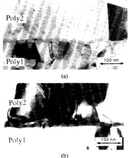
Fig. 3. The TEM micrograph of polyoxide-polysilicon interface of (a) the median-doped polyoxide and (b) the heavily doped polyoxide
- 1 1 I I I I I I 5 I
0 LO 80 120 160 200
Stressing Tlrne (sec)
Fig. 2.
a constant current of capacitor is 1.256 X 10
The gate voltage shift versus stressing time of polyoxides under 100-pA/cmZ stressing. The area of polyoxide cm2.
in Fig. 2. The gate voltage shifts in both polarities of the median doped polyoxide are much larger than those of
the heavily doped polyoxide. Also, for the heavily doped
polyoxide, the voltage shifts for both polarities are almost the same. The results in Figs. 1 and 2 indicate that the heavily doped polyoxide has a better quality as well as a smoother polysilicon-polyoxide interface as compared to the median-doped polyoxide. Fig. 3(a) and (b) shows the cross-sectional transmission electron microscopy micro- graphs of the median-doped and heavily doped polyoxides, respectively. It is seen that the polysilicon-polyoxide in-
terfaces of the heavily doped polyoxide are much smoother than those of the median-doped polyoxide. This is be- cause during the low-temperature wafer loading and N,
preannealing process
[4],
the grain sizes of the heavilydoped polysilicon were significantly increased and the number of grain boundaries were reduced as compared to the case of the median-doped polysilicon, as seen from the figure. This results in a smoother polyoxide-polysili- con interface.
IV. CONCLUSION
The low-temperature wafer loading and N, preanneal- ing process can produce a smoother surface of the heavily doped polysilicon such that the lower polysilicon-poly-
oxide interface is smoother than that of the upper one. As
a result, the heavily doped polyoxide has less tunneling
current and a higher Ehd value when poly 2 is positively
biased. This asymmetrical J-E characteristic may have
special advantages for the application of EEPROM [l].
REFERENCES
[l] T. Ono, T. Mori, T. Ajioka, and T. Takayashiki, “Studies of thin poly-Si oxides for E and E’PROM,” in IEDM Tech. Dig., 1985, pp. R. M. Anderson and D. R. Kerr, “Evidence for surface asperity mechanisn of conductivity in oxide grown on polycrystalline silicon,” J. Appl. Phys., vol. 48, pp. 4834-4836, 1977.
L. Faraone, “Thermal SiO, films on n + polycrystalline silicon: Electrical conduction and breakdown,” IEEE Truns. Electron De-
uices, vol. ED-33, pp. 1785-1794, 1986.
S. L. Wu, C. L. Lee, and T. F. Lei, “Characterization of ultra-thin oxide prepared by low-temperature wafers loading and nitrogen pre-annealing before oxidation,” J. Appl. Phys., vol. 68, pp. 380-383.
[2] [3] [4]