990 IEEE ELECTRON DEVICE LETTERS, VOL. 28, NO. 11, NOVEMBER 2007
Improved Electrical Characteristics and Reliability of
MILC Poly-Si TFTs Using Fluorine-Ion Implantation
Chih-Pang Chang and YewChung Sermon Wu
Abstract—In this letter, fluorine-ion (F+) implantation was employed to improve the electrical performance of metal-induced lateral-crystallization (MILC) polycrystalline-silicon thin-film transistors (poly-Si TFTs). It was found that fluorine ions mini-mize effectively the trap-state density, leading to superior electri-cal characteristics such as high field-effect mobility, low threshold voltage, low subthreshold slope, and highON/OFF-current ratio. F+-implanted MILC TFTs also possess high immunity against the hot-carrier stress and, thereby, exhibit better reliability than that of typical MILC TFTs. Moreover, the manufacturing processes are simple (without any additional thermal-annealing step), and compatible with typical MILC poly-Si TFT fabrication processes. Index Terms—Fluorine-ion implantation, metal-induced lateral crystallization (MILC), polycrystalline-silicon thin-film transis-tors (poly-Si TFTs).
I. INTRODUCTION
L
OW-TEMPERATURE polycrystalline-silicon thin-film transistors (poly-Si TFTs) have attracted considerable interest for their use in active-matrix liquid-crystal displays because they exhibit good electrical properties and can be integrated in peripheral circuits on inexpensive glass substrates [1]. As poly-Si TFTs require glass substrates, intensive studies have thus been carried out, reducing the crystallization tem-perature of amorphous silicon (α-Si) films. Ni-metal-induced lateral crystallization (MILC) is one of these efforts. In MILC, Ni islands are selectively deposited on top of α-Si films and allowed to crystallize at a temperature below 600◦C [2], [3].Unfortunately, the poly-Si grain boundaries trap Ni and NiSi2precipitates, thus increasing leakage current and shifting
the threshold voltage [4]–[8]. A hydrogen plasma-treatment process has been utilized to reduce the trap states of poly-Si film to improve the device performance [9]. However, not only was it difficult to control hydrogen concentration in the poly-Si film but the formed Si–H bonds were also not strong enough to avoid the hot-carrier generation. Fluorine (F)-ion incorporation has been applied in the manufacturing of many electronic devices [10], [11]. On poly-Si TFTs implanted with fluorine, the Si–F bonds can eliminate the trap-state density, thus enhancing the performance of n-channel TFTs.
In this letter, a new manufacturing method for MILC poly-Si TFTs using fluorine-ion implantation was proposed. This
un-Manuscript received July 3, 2007. This work was supported by the Na-tional Science Council of China under Grants NSC95-2221-E009-087MY3 and NSC95-2221-E009-125. The review of this letter was arranged by Editor J. Sin. The authors are with the Department of Materials Science and Engineer-ing, National Chiao Tung University, Hsinchu 300, Taiwan, R.O.C. (e-mail: [email protected]).
Digital Object Identifier 10.1109/LED.2007.906803
complicated and effective method involves implanting fluorine atoms into poly-Si films, which produces MILC poly-Si TFTs of high performance and high reliability.
II. EXPERIMENT
A 100-nm-thick undoped (α-Si) layer was deposited onto a 500-nm-thick oxide-coated silicon wafer by low-pressure chemical-vapor-deposition (LPCVD) system. The photoresist was patterned to form desired Ni lines, and a 20-Å-thick Ni film was deposited on the α-Si, subsequently annealed at 540 ◦C for 18 h to form the MILC poly-Si film. To reduce Ni contamination, the unreacted Ni metal was removed by chemical etching. The islands of poly-Si regions on the wafers were defined by reactive-ion etching; fluorine ions were then implanted into the MILC film. The projection range of fluorine ions was set at the middle of MILC layer. The dosage of fluorine ions and ion-accelerating energy was 2× 1013 cm−2 and 30 KeV, respectively. Next, a 100-nm-thick gate insulator was deposited by plasma-enhanced CVD. Then a 200-nm-thick poly-Si film was deposited for gate electrodes by LPCVD. After defining the gate, self-aligned 40 KeV P ions were implanted at a dose of 5× 1015cm−2to form the source/drain and gate. The F+-implanted MILC film and the P-implanted
source/drain/gate were then annealed/activated at 600 ◦C for 24 h. Moreover, the manufacturing processes without any ad-ditional thermal annealing step and compatible with typical MILC poly-Si TFT fabrication processes.
III. RESULTS ANDDISCUSSIONS
Fig. 1 shows the ID–VGtransfer characteristics for the MILC poly-Si TFTs, with and without F+implantation. The measured and extracted key device parameters are summarized in Table I. The performance of F+-implanted TFTs was far superior to
that of MILC TFTs. This indicates the trap-state density (Nt) was effectively terminated using F+ implantation. The
trap-state density was extracted using Levinson’s and Proano’s method, which can estimate the Nt from the slope of the linear segment of ln[IDS/(VGS–VFB)] versus 1/(VGS–VFB)2
at low VDS and high VGS, where VFB is defined as the gate
voltage that yields the minimum drain–current at VDS= 0.1
[12], [13]. The trap density of F+-implanted MILC TFTs is 4.24× 1012 cm−2, which is less than that of MILC TFTs (6.29× 1012 cm−2). The reduction in Nt values implies that those defects have been terminated using F+ implantation. As a result, the carrier mobility increases. The minimum
OFF-current of the F+-implanted device, however, did not
CHANG AND WU: IMPROVED ELECTRICAL CHARACTERISTICS AND RELIABILITY OF MILC POLY-Si TFTs 991
Fig. 1. Typical IDS–VGStransfer characteristics of the MILC poly-Si TFTs,
with and without F+implantation.
TABLE I
DEVICECHARACTERISTICS OF THEMILC POLY-Si TFTs, WITH ANDWITHOUTF+IMPLANTATION
change much. Similar performances and defects have been previously reported in other poly-Si TFTs that were passivated by the F+implantation [14]–[16].
In MILC poly-Si, there are two kinds of defects related to trap-state density: 1) Ni-related defects and 2) grain-boundary defects. Most of Ni-related defects were located at poly-Si/ buffer-oxide interface and grain boundaries, which trap Ni and NiSi2 precipitates [4]–[8]. Ni-related defects would
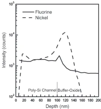
de-grade electric performance because the trap states introduced dangling and strain bonds. Secondary-ion mass spectroscopy (SIMS) was used to study the distribution of Ni and F. Fig. 2 shows the depth profile of the F+-implanted MILC poly-Si/ buffer-oxide structure after thermal annealing at 600 ◦C for 24 h. High-Ni and high-F contents are both present at the MILC poly-Si/buffer-oxide interface. This observation suggested that F ions have diffused to the interface/boundaries to terminate Ni-related trap states and lead to improve electrical characteristics. On the other hand, the trap states in the grain boundaries will also increase the leakage current. Use of F atoms to fluorinate Si films can improve performance and reliability of poly-Si TFTs [16]. This is because F atoms can terminate dangling bonds and replace weak bonds in the grain boundaries and
Fig. 2. SIMS depth profile of nickel and fluorine in the structure of MILC poly-Si channel/buffer-oxide.
Fig. 3. Threshold-voltage variation versus stress time for the MILC poly-Si TFTs, with and without F+implantation.
SiO2/poly-Si interface and, thus, reduce the trap states in the
poly-Si channel. As a result, the carrier mobility increases due to the decrease in the boundary scattering by passivation-of-boundaries defects. However, the minimum OFF-currents were nearly unchanged [14]–[16].
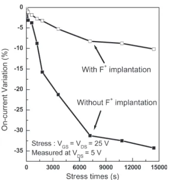
The other important issue of poly-Si TFTs is their reliability, which was examined under hot-carrier stress. As shown in Figs. 3 and 4, the threshold voltage and the ON-current of TFTs were degraded, because dangling bonds are created due to the trapping of electrons at weak Si–Si and Si–H bonds [17], [18]. Compared with those of typical MILC TFTs, the threshold voltage andON-current degradations of F+-implanted
992 IEEE ELECTRON DEVICE LETTERS, VOL. 28, NO. 11, NOVEMBER 2007
Fig. 4. ON-current degradation versus stress time for the MILC poly-Si TFTs, with and without F+implantation.
MILC TFTs are greatly improved by the implantation process. F+-implanted MILC TFTs also possess high immunity against the hot-carrier stress and, thereby, exhibit lower ∆VTH and
∆ION/ION than that of typical MILC TFTs. In other words,
weaker Si–H and Si–Si bonds were replaced by stronger Si–F bonds, which could not be broken under hot-carrier stress, thus leading to improved electrical reliability.
Electrical properties of the F+-implanted MILC TFTs with heavy implantation dosages (2× 10¹⁴ and 2× 1015 cm−2) were also studied in this letter. It is found that the electrical characteristics of MILC TFT are degraded as the implantation dosage increases. When the dosage reached 2× 1015 cm−2, the device performance was very poor. This is because, when the implantation dosages are higher than Si solid solu-bility, the trap-state density and fluorine clusters increased with the dosage [19].
IV. CONCLUSION
An investigation of the effects of F+-implantation process
on the electrical characteristics and reliability of MILC poly-Si TFTs has led to the development of a simple effective process for improving the TFT electrical properties. Results show that, compared with typical MILC TFTs, F+-implanted
TFTs exhibit higher field-effect mobility, superior subthreshold slope, lower threshold voltage, higher ON/OFF-current ratio, and lower trap-state density (Nt). It was also found that F+ -implantation process can greatly alleviate the threshold voltage and the ON-current degradations under hot-carrier stress. F+ -implanted MILC TFTs possess high immunity against the hot-carrier stress and, thereby, exhibit lower ∆VTHand ∆ION/ION
than that of typical MILC TFTs. This is because the weaker Si–H and Si–Si bonds were replaced by stronger Si–F bonds, which could not be broken under hot-carrier stress, thus leading to improved electrical reliability.
ACKNOWLEDGMENT
The authors would like to thank the technical support from the National Nano Device Laboratory of NSC and Nano Facil-ity Center of National Chiao Tung UniversFacil-ity.
REFERENCES
[1] M. Stewart, R. S. Howell, L. Pires, and M. K. Hatalis, “Polysilicon TFT technology for active matrix OLED displays,” IEEE Trans. Electron
Devices, vol. 48, no. 5, pp. 845–851, May 2001.
[2] S. W. Lee and S. K. Joo, “Low temperature poly-Si thin-film transis-tor fabrication by metal-induced lateral crystallization,” IEEE Electron
Device Lett., vol. 17, no. 4, pp. 160–162, Apr. 1996.
[3] Z. Meng, M. Wang, and M. Wong, “High performance low tempera-ture metal-induced unilaterally crystallized polycrystalline silicon thin film transistors for system-on-panel applications,” IEEE Trans. Electron
Devices, vol. 47, no. 2, pp. 404–409, Feb. 2000.
[4] P. J. van der Zaag, M. A. Verheijen, S. Y. Yoon, and N. D. Young, “Ex-planation for the leakage current in polycrystalline-silicon thin-film tran-sistors made by Ni-silicide mediated crystallization,” Appl. Phys. Lett., vol. 81, no. 18, pp. 3404–3406, Oct. 2002.
[5] G. A. Bhat, Z. Jin, H. S. Kwok, and M. Wong, “Effects of longitudinal grain boundaries on the performance of MILC-TFTs,” IEEE Electron
Device Lett., vol. 20, no. 2, pp. 97–99, Feb. 1999.
[6] Z. Jin, K. Moulding, H. S. Kowk, and M. Wong, “Performance of thin-film transistors with ultrathin Ni-MILC polycrystalline silicon channel layers,”
IEEE Electron Device Lett., vol. 20, no. 4, pp. 167–169, Apr. 1999.
[7] G. A. Bhat, H. S. Kwok, and M. Wong, “Behavior of the drain leakage current in metal-induced laterally crystallized thin film transistors,” Solid
State Electron., vol. 44, no. 7, pp. 1321–1324, Jul. 2000.
[8] D. Murley, N. Young, M. Trainor, and D. McCulloch, “An investigation of laser annealed and metal-induced crystallized polycrystalline silicon thin-film transistors,” IEEE Trans. Electron Devices, vol. 48, no. 6, pp. 1145– 1151, Jun. 2001.
[9] I. W. Wu, W. B. Jackson, T. Y. Huang, A. G. Lewis, and A. C. Chiang, “Passivation kinetics of two types of defects in polysilicon TFT by plasma hydrogenation,” IEEE Electron Device Lett., vol. 12, no. 5, pp. 181–183, May 1991.
[10] C. H. Tu, T. C. Chang, P. T. Liu, C. Y. Yang, H. C. Liu, W. R. Chen, Y. C. Wu, and C. Y. Chang, “Improvement of electrical characteristics for fluorine-ion-implanted poly-Si TFTs using ELC,” IEEE Electron Devices
Lett., vol. 27, no. 4, pp. 262–264, Apr. 2006.
[11] C. H. Tu, T. C. Chang, P. T. Liu, H. W. Zan, Y. H. Tai, C. Y. Yang, Y. C. Wu, H. C. Liu, W. R. Chen, and C. Y. Chang, “Enhanced perfor-mance of poly-Si thin film transistors using fluorine ions implantation,”
Electrochem. Solid-State Lett., vol. 8, no. 9, pp. G246–G248, Jul. 2005.
[12] J. Levinson, G. Este, M. Rider, P. J. Scanlon, F. R. Shepherd, and W. D. Westwood, “Conductivity behavior in polycrystalline semiconduc-tor thin film transissemiconduc-tors,” J. Appl. Phys., vol. 53, no. 2, pp. 1193–1202, Feb. 1982.
[13] R. E. Proano, R. S. Misage, and D. G. Ast, “Development and electrical properties of undoped polycrystalline silicon thin-film transistors,” IEEE
Trans. Electron Devices, vol. 36, no. 9, pp. 1915–1922, Sep. 1989.
[14] H. N. Chern, C. L. Lee, and T. F. Lei, “The effects of fluorine passiva-tion on polysilicon thin-film transistors,” IEEE Trans. Electron Devices, vol. 41, no. 5, pp. 698–702, May 1994.
[15] C. H. Kim, S. H. Jung, J. S. Yoo, and M. K. Han, “Poly-Si TFT fabricated by laser-induced in-situ fluorine passivation and laser doping,” IEEE Electron Device Lett., vol. 22, no. 8, pp. 396–398, Aug. 2001.
[16] S. D. Wang, W. H. Lo, and T. F. Lei, “CF4 plasma treatment for fabrication high-performance and reliable solid-phase-crystallized poly-Si TFTs,” J. Electrochem. Soc., vol. 152, no. 9, pp. G703–G706, Jul. 2005.
[17] S. Banerjee, R. Sundraesan, H. Shichijo, and S. Malhi, “Hot-electron degradation of n-channel polysilicon MOSFETs,” IEEE Trans. Electron
Devices, vol. 35, no. 2, pp. 152–157, Feb. 1988.
[18] M. Hack, A. G. Lewis, and I. W. Wu, “Physical models for degradation effects in polysilicon thin-film transistors,” IEEE Trans. Electron Devices, vol. 40, no. 5, pp. 890–897, May 1993.
[19] C. H. Tu, T. C. Chanf, P. T. Liu, C. H. Chen, C. Y. Yang, Y. C. Wu, H. C. Liu, L. T. Chang, C. C. Tsai, S. M. Sze, and C. Y. Chang, “Electrical enhancement of solid phase crystallized poly-Si thin-film transistors with fluorine ion implantation,” J. Electrochem. Soc., vol. 153, no. 9, pp. G815– G818, Jul. 2006.