Synthetic Metals 158 (2008) 130–134
High-efficiency blue multilayer polymer light-emitting diode
fabricated by a general liquid buffer method
Shin-Rong Tseng
a, Hsin-Fei Meng
a,∗, Chi-Hung Yeh
b, Huan-Chung Lai
b, Sheng-Fu Horng
b,
Hua-Hsien Liao
b, Chain-Shu Hsu
c, Li-Chi Lin
daInstitute of Physics, National Chiao Tung University, 1001 Ta Hsueh Road, Hsinchu 300, Taiwan, ROC bInstitute of Electronics Engineering, National Tsing Hua University, Hsinchu 300, Taiwan, ROC
cDepartment of Applied Chemistry, National Chiao Tung University, Hsinchu 300, Taiwan, ROC dDelta Optoelectronics, Science-Based Industrial Park, Hsinchu 308, Taiwan, ROC
Received 29 October 2007; received in revised form 20 December 2007; accepted 21 December 2007 Available online 20 February 2008
Abstract
A bright, highly efficient blue polymer light-emitting diode is fabricated by spin-coating with multilayer structure. By introducing a liquid buffer layer, the dissolution problem is overcome successfully. This general method can be applied to fabricate arbitrary polymer multilayer structure, in particular the addition of the carrier blocking layers to balance the electron and hole currents and improve the device efficiency. By adding an electron-blocking layer, the external quantum efficiency for blue emission can be increased to 5.5% (9.1 cd/A) which is even higher than the theoretical limit of 5%. The luminance reaches 26,530 cd/m2and the Commission Internationale de L’Eclairage (CIE) coordinates is (0.15, 0.23).
Further more the lifetime is increased by three times relative to the single layer device. © 2007 Elsevier B.V. All rights reserved.
Keywords: Polymer light-emitting diodes; Multilayer; Blue; White; High efficiency
Conjugated polymer light-emitting diodes (PLED) attract a lot of interests due to their easy solution process and potentially high-emission efficiency. Therefore it is viewed as the material for the next generation of flat panel display [1]. One promis-ing way for display application is uspromis-ing white PLED combined with colorfilters. For this purpose highly efficient blue PLED is a prerequisite, because through energy transfer process one can achieve white PLED by using the blue emitters as host and red/green emitters as dopants[2–4]. Efficient blue PLED remains a challenge so far partly due to their large band-gap and difficulty in charge balance. Many efforts have been made to improve efficiency by molecular design [5,6]and molecu-lar weight selection [7]. Recently phosphorescent blue PLED achieved efficiency as high as 22 cd/A[8], but till now the highest efficiency for fluorescent blue PLED is around 3 cd/A[9,10]. It is still far below the blue small-molecular organic light-emitting diodes (OLED)[11], which take advantages of the multilayer
∗Corresponding author. Tel.: +886 5731955.
E-mail address:[email protected](H.-F. Meng).
structure for balanced electron and hole currents. The main rea-son for this efficiency gap is that the solution process itself causes dissolution between spin-coated layers. Consequently for PLED the multilayer design is incompatible with the easy solution process so far. This dilemma unfortunately implies that the advantage of separating different functions such as charge injection, charge transport, and light emission into different lay-ers cannot be used to improve PLED efficiency. Many strategies were attempted to overcome the dilemma and make multilayer PLEDs[12–20]. Recently, we introduce a new liquid buffer layer (BL) method[21] which completely prevents the dissolution between solution-processed polymer layers and use it to add a hole blocking layer to the hole-dominated emissive polymers to improve the efficiency. In this work we apply this BL method to add an electron-blocking layer to the electron-dominated blue polymers. The efficiency and brightness are several times higher than the results reported by the Dow Chemical Company.
The material of the BL must be a viscous non-solvent liq-uid with relatively low-boiling point. The protection capability is directly related to the viscosity. Before depositing the next polymer layer over an existing soluble polymer surface, the BL
0379-6779/$ – see front matter © 2007 Elsevier B.V. All rights reserved. doi:10.1016/j.synthmet.2007.12.016
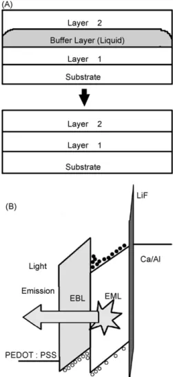
is first spin-coated. The next layer is then spun on the top of the liquid surface of the BL. Because the viscosity of the BL is much higher than the usual solvent, the next layer will initially float over the BL instead of mixing with it. The polymer underneath is therefore protected by the BL against the solvent of the next layer. During the spinning most of the solvent of the next layer and part of the liquid BL are evaporated, resulting in a double-layer structure with possibly some residue of the BL in between. The residual BL is removed by baking in vacuum. Therefore, besides the high viscosity low-boiling point and small-molecule weight of BL are also important for easy removal by baking. We found that 1,2-propylene glycol combines the unique properties of high viscosity (248η/mPa s at 0◦C, 40.4η/mPa s at 25◦C) and low-boiling point (188◦C), which are crucial for the protec-tion and subsequent removal of BL as stated above. Despite of low-molecular weight (76.095 amu), 1,2-propylene glycol derives its high viscosity from strong hydrogen bond which for-tunately diminishes with temperature rapidly. Prior to spinning, 1,2-propylene glycol is cooled to ensure enough initial viscosity. The exact optimal temperature depends on the material of layer 1, because different polymers have different degrees of adhesion with 1,2-propylene glycol. It is generally between 0 and 10◦C. We are not able to measure the steady state thickness of the buffer liquid during spinning. However it is judged to be at least sev-eral micron thick considering the high viscosity.Fig. 1(A) shows the steps of the BL method. This method is used to fabricate a bilayer blue PLED with layer 1 as the electron-blocking layer (EBL) and layer 2 as the emissive layer (EML). The energy bands and carrier recombination are schematically shown inFig. 1(B). The method is very easy to apply and does not involve and pro-cess other than spin-coating and baking. There is no need to design and synthesize new functional materials. One can gener-ally choose the combinations of existing materials with desired properties as long as they can be dissolved in some solvent. Note that alcohols with multiple OH groups have been used as dopants in the poly-(3,4-ethylenedioxythiophene):poly-(styrene sulfonate) (PEDOT:PSS) anode to improve the conductivity and device performance[22,23]. The effect of the buffer liquid like 1,2-propylene glycol on our PLED is however independent of the doping effect since the buffer liquid does not touch the PEDOT:PSS layer at all.
In this work, all the PLED devices were fabricated on glass substrates with layers which include a PEDOT:PSS layer on a patterned ITO layer. Before depositing the emissive layer, poly[(9,9-dioctylfluorenyl-2,7-diyl)-co-(4,4’-(N-(4-sec y-butylphenyl))diphenylamine)] (TFB with chemical structure shown inFig. 2(A); purchased from American Dye Source) are spin-coated on the PEDOT:PSS layer as an hole-transport layer (HTL) and electron-blocking layer (EBL). LUMATION BP105 (electron affinity (EA)/ionization potential (IP)= 3.0/5.8 eV) from the Dow Chemical Company is chosen to be the blue poly-mer. BP105 is currently very good blue polymer for PLED. Even so the electron–hole balance is far from perfect. In single layer LED the current is dominated by electron current because of the high electron mobility and large hole injection barrier. Such imbalance is evidenced by the much smaller hole-only current than the LED current to be shown inFig. 2(B). Four kinds of
Fig. 1. (A) Double-layer polymer films fabrication process by inserting an inter-mediate liquid buffer layer (BL) of 1,2 propylene glycol. The liquid BL can be removed by baking in vacuum and (B) schematic electronic energy profile for the double-layer device structure.
devices are made to present the advantage of the buffer method. The first two are ITO/PEDOT: PSS/TFB/EML/Cathode made by the BL method and the spin-rinse method[14]. The second two are ITO/PEDOT: PSS/EML/Cathode made by pure BP105 or BP105:TFB blend (10:1). The ITO substrates are cleaned and the surfaces are treated by oxygen plasma followed by spin-coating 50 nm of PEDOT:PSS. PEDOT:PSS film is baked at 200◦C for 5 min in vacuum environment (10−3Torr). TFB film (30 nm) is spin-coated on PEDOT:PSS film (1% in xylene) and annealed at 180◦C in vacuum for 40 min. For the BL method, a 67 nm BP105 film is spin-coated (2% in xylene) over the liquid buffer covering TFB. The double-layer device is baked at 120◦C for 1 h in vacuum to remove the residue 1,2-propylene glycol. Since the size of 1,2-propylene glycol molecules is about the same as com-mon organic solvents like xylene, there should be no problem for them to diffuse across the layer 2 polymer during anneal-ing. In fact any significant residue of 1,2-propylene glycol at the interface would be detrimental to the device performance. The excellent performance to be discussed below is another evidence for the complete removal of the buffer liquid. There is no loss
Fig. 2. The performances of blue PLED: single layer BP105 (solid circle), double-layer TFB/BP105 with BL process (open circle), spin-rinsed TFB/BP105 (solid triangle), BP105 blending with TFB (open triangle). (A) The current efficiency. Inset are the EL spectrum and TFB chemical structure and (B) the luminance. Inset is the current density. Note the current for hole-only BP105 device (PEDOT/BP105/Al, solid star) is much smaller than the single layer LED current, indicating dominance of electron current without blocking layer.
in the double-layer film thickness compared with the sum of the two individual films within the error of thickness measurement. In other words, the inter-diffusion of the two polymers is less than the experimental error of the individual thickness, which is about 5 nm. For the spin-rinsing method, a very thin TFB layer (about 10 nm) was achieved by spin-rinsing the TFB layer with pure xylene to remove the remaining soluble part. A 67 nm BP105 film is then spin-coated on the spin-rinsed TFB layer and baked at 120◦C for 40 min in vacuum. For the other devices the EML films are baked in vacuum for 40 min at 120◦C. Finally all the devices are coated with LiF/Ca/Al cathode and pack-aged in the glove box. The film thicknesses are measured by a Kosaka ET4000 Surface Profiler. The electroluminescence (EL) spectra and current–luminance–voltage (I–L–V) characteristics are measured by a Photo Research PR650 spectrophotometer integrated with Keithley 2400 multi-meter.
Fig. 2shows the results of the four kinds of blue PLEDs. A is ITO/PEDOT:PSS/BP105/LiF/Ca/Al, B is ITO/PEDOT: PSS/TFB/(BL)/BP105 /LiF/Ca/Al, C is ITO/PEDOT:PSS/spin-rinsed TFB/BP105 /LiF/Ca/Al, and D is ITO/PEDOT/BP105:
TFB/Ca/Al. B and C have EBL/EML bilayer structure while A and D are single layer devices. From the EL spectrum shown in inset ofFig. 2(A), the emission colors are almost the same in all devices, indicating TFB only affects carrier transport. Compar-ing devices A and B, the maximum current efficiency is enhanced from 2.7 to as high as 9.1 cd/A by the double-layer structure using BL method. The corresponding external quantum effi-ciency (EQE) is enhanced from 1.5 to 5.5%, which is even higher than the theoretical limit of 5%, indicating the electron and hole currents are balanced in the EML. The current does not become smaller, probably due to the emergence of large recombination current occurring in the electron accumulation region near the TFB/BP105 barrier. The maximum luminance is increased from 6675 to 26,530 cd/m2. As for device C the efficiency is moder-ately enhanced from 2.7 to 3.5 cd/A, far behind the dramatic case of device B. The spin-rinsed TFB is either too thin to block the electrons effectively or is re-dissolved by the BP105 solution and leaves a mixed area near the PEDOT:PSS and BP105 inter-face. In fact the result for device D is very similar to device C, strongly suggesting the second scenario above. From the above results, BL method is far superior than spin-rinsing and blending for device performance. We believe that this is because a sharp interface between two polymers is required for a good device and such interface can only be realized by the liquid buffer method due to the excellent protection capability.Fig. 3shows the life-time of single layer (A) and bilayer (B) devices. The devices were tested at room temperature and ambient pressure under the condition of the constant dc current. Initial luminances for the devices are about 1000 cd/m2. By linear fitting we estimate the lifetime are 600 min of B device and 200 min of A device. In addition to high efficiency the lifetime of the bilayer device is increased by three times. This might be because the TFB layer prevents the degradation of BP105 layer by the acid PEDOT:PSS [24]. Based on the high efficiency blue PLED we introduce green and red guest dopants to the blue polymer host to make white PLED. The guest polymers are also polyfluorene copolymer from the LUMATION series of the Dow Chemical Company with EA/IP = 2.19/4.56 eV for the green and 2.84/5.12 eV for the red. The concentrations are 1.7 wt% for green and 0.55 wt%
Fig. 3. The lifetime of BP105 PLED with TFB (open circle) and without TFB (solid circle).
Table 1
Performance of PLEDs in this work
Label Maximum current efficiency (cd/A) Maximum EQE (%) Maximum luminance (cd/m2)
BP105(A) 2.7 (at 10 V) 1.50 6,675 (at 11 V)
TFB/BP105(B) 9.1 (at 5.5 V) 5.54 26,530 (at 8 V)
Spin-rinsed TFB/BP105(C) 3.5 (at 8 V) 1.85 21,546 (at 12 V)
BP105:TFB(D) 3.92 (at 7 V) 2.25 21,924 (at 11 V)
White PLED 3.0 (at 10 V) 1.45 5,633 (at 13 V)
TFB/White PLED 4.7 (at 10 V) 2.46 21,180 (at 13 V)
for red in the host. The film thicknesses of white EML are 55 and 70 nm with and without TFB layer.Fig. 4shows the results of white PLEDs with and without TFB as EBL applied by BL method. The CIE coordinates are (0.29, 0.38) for single layer and (0.27, 0.34) for bilayer white PLED. The maximum luminance is increased from 5633 to 21,180 cd/m2. The current efficiency is enhanced from 3.0 to 4.7 cd/A, and the corresponding EQE from 1.45 to 2.46%.Table 1shows the maximum current effi-ciency, its corresponding EQE and maximum luminance of all the devices.
In conclusion we develop a buffer layer method to fabricate all-solution-processed multilayer polymer device. By applying
Fig. 4. The performances of white PLED with TFB (open circle) and without TFB (solid circle). (A) The current efficiency. Inset is the EL spectrum and (B) the luminance. Inset is the current density.
this method to add a hole-transport/electron-blocking layer to balance the electron and hole currents of blue PLED, the effi-ciency is improved to nearly the theoretical limit. This method can be applied to not only PLED but also other solution-process multilayer polymer devices like solar cells which need the inter-face to increase the efficiency.
Acknowledgements
We thank the Dow Chemical Company for supplying the LUMATION series polymers. This work is supported by the National Science Council of the Republic of China (No. NSC 96-2112-M-009-036).
References
[1] R.H. Friend, R.W. Gymer, A.B. Holmes, J.H. Burroughes, R.N. Marks, C. Taliani, D.D.C. Bradley, D.A.D. Santos, J.L. Bredas, M. Logdlund, W.R. Salaneck, Nature 397 (1999) 121.
[2] M. Granstrom, O. Inganas, Appl. Phys. Lett. 68 (1996) 147. [3] B. Hu, F. Karasz, J. Appl. Phys. 93 (2003) 1995.
[4] J. Huang, W.J. Hou, J.H. Li, G. Li, Y. Yang, Appl. Phys. Lett. 89 (2006) 133509.
[5] X. Gong, W. Ma, J.C. Ostrowski, G.C. Bazan, D. Moses, A.J. Heeger, Adv. Mater. 16 (2004) 615.
[6] F.I. Wu, P.I. Shih, C.F. Shu, Y.L. Tung, Y. Chi, Macromolecules 38 (2005) 9028.
[7] K.H. Weinfurtner, H. Fujikawa, S. Tokito, Y. Taga, Appl. Phys. Lett. 76 (2000) 2502.
[8] M.K. Mathai, V.E. Choong, S.A. Choulis, B. Krummacher, F. So, Appl. Phys. Lett. 88 (2006) 243512.
[9] C.D. Muller, A. Falcou, N. Reckefuss, M. Rojahn, V. Wiederhirn, P. Rudati, H. Frohne, O. Nuyken, H. Becker, K. Meerholz, Nature 421 (2003) 829.
[10] W. Wu, M. Inbasekaran, M. Hudack, D. Welsh, W. Yu, Y. Cheng, C. Wang, S. Kram, M. Tacey, M. Bernius, R. Fletcher, K. Kiszka, S. Munger, J. O’Brien, Microelectron. J. 35 (2004) 343.
[11] C.H. Liao, M.T. Lee, C.H. Tsai, C.H. Chen, Appl. Phys. Lett. 86 (2005) 203507.
[12] Z. Liang, O.M. Cabarcos, Adv. Mater. 16 (2004) 823.
[13] W. Ma, P.K. Iyer, X. Gong, B. Liu, D. Moses, G.C. Bazan, A.J. Heeger, Adv. Mater. 17 (2005) 274.
[14] J.S. Kim, R.H. Friend, I. Grizzi, J.H. Burroughes, Appl. Phys. Lett. 87 (2005) 023506.
[15] G.K. Ho, H.F. Meng, S.C. Lin, S.F. Horng, C.S. Hsu, L.C. Chen, S.M. Chang, Appl. Phys. Lett. 85 (2004) 4576.
[16] C.C. Huang, H.F. Meng, G.K. Ho, C.H. Chen, C.S. Hsu, J.H. Huang, S.F. Horng, B.X. Chen, L.C. Chen, Appl. Phys. Lett. 84 (2004) 1195. [17] T.W. Lee, M.G. Kim, S.Y. Kim, S.H. Park, O. Kwon, T. Noh, T.S. Oh, Appl.
[18] D.C. M¨uller, T. Braig, H.G. Nothofer, M. Arnoldi, M. Gross, U. Scherf, O. Nuyken, K. Meerholz, ChemPhysChem 1 (2000) 207.
[19] S.A. Choulis, V.E. Choong, A. Patwardhan, M.K. Mathai, F. So, Adv. Funct. Mater. 16 (2006) 1075.
[20] X. Gong, S. Wang, D. Moses, G.C. Bazan, A.J. Heeger, Adv. Mater. 17 (2005) 2053.
[21] S.R. Tseng, S.C. Lin, H.F. Meng, H.H. Liao, C.H. Ye, H.C. Lai, S.F. Horng, C.S. Hsu, Appl. Phys. Lett. 88 (2006) 163501.
[22] S.K.M. Jonsson, J. Birgerson, X. Crispin, G. Greczynski, W. Osikowicz, A.W. Denier van der Gon, W.R. Salaneck, M. Fahlman, Synth. Met. 139 (2003) 1.
[23] X. Crispin, F.L.E. Jakobsson, A. Crispin, P.C.M. Grim, P. Andersson, A. Volodin, C. van Haesendonck, M. Van der Auweraer, W.R. Salaneck, M. Berggren, Chem. Mater. 18 (2006) 4354.
[24] A. van Dijken, A. Perro, E.A. Meulenkamp, K. Brunner, Org. Electron. 4 (2003) 131.