國 立 交 通 大 學
光 電 工 程 學 系 碩 士 班
碩 士 論 文
Up-Conversion 螢光量測系統的架設和
極小尺寸氮化銦奈米棒陣列的變溫螢光
量測
The Construction of Up-Conversion
Luminescence System and
Temperature-dependent PL Study of InN
Nanorod Arrays with Critical Size
研 究 生:劉育昇
指導教授:安惠榮 教授
Up-Conversion 螢光量測系統的架設和極小尺寸
氮化銦奈米棒陣列的變溫螢光量測
The Construction of Up-Conversion Luminescence
System and Temperature-dependent PL Study of
InN Nanorod Arrays with Critical Size
研 究 生:劉育昇 Student:Yu-Sheng Liu
指導教授:安惠榮 教授 Advisor:Prof.Hyeyoung Ahn
國 立 交 通 大 學
光電工程學系碩士班
碩 士 論 文
A Thesis
Submitted to Department of Photonics and
Institute of Electro-Optical Engineering
College of Electrical Engineering
National Chiao Tung University
In partial Fulfillment of the Requirements
for the Degree of
Master of Science
in
Electro-Optical Engineering
July 2013
Hsinchu, Taiwan, Republic of China
I
The Construction of Up-Conversion Luminescence System and
Temperature-dependent PL Study of InN Nanorod Arrays with
Critical Size
Student : Yu-Sheng Liu Advisors : Prof. Hyeyoung Ahn
Institute of Electro-Optical Engineering National Chiao Tung University
Abstract
Photoluminescence (PL) can characterize the emission property of various semiconductors, which is in turn used to understand the purity, crystalline quality, disorders, etc. of semiconductors such as InGaAs and InP. In this work, we have intensively studied the PL from vertically aligned indium nitride (InN) nanorods (NRs) grown on Si (111) substrates. In particular, the abnormal behavior of PL from InN NRs with the rod diameter comparable to the surface electron accumulation layer was observed. Exceptionally large activation energy of the NRs with the critical diameter implies that holes within these narrow NRs need to surpass the band bending near the surface in order to recombine with electrons accumulated in the surface layer. Time-resolved PL (TRPL) also plays an important role in providing the information of dynamic behavior of radiative recombination of semiconductors. However, time-correlated single photon counting method, which is typically used for life science, has rather long time resolution for elucidating the dynamic phenomena of semiconductors. In the second part of this thesis, the development of up-conversion PL system is introduced. The basic concept of sum frequency generation and its application to the ultrafast luminescence spectroscopy are
II
described in detail. Furthermore, the optical configuration, photon counting technique, and the automatic control of the up-conversion PL system are demonstrated. The theoretical calculation of TRPL signal level are compared to the preliminary experimental results of our system.
III
Content
Abstract ... I
Content ... III
List of Figures ... VI
List of table ... X
Chapter 1 Introduction ... 1
1.1 Background ... 1 1.2 Motivation ... 2 1.3 Thesis Structure ... 3Chapter 2 Design of Up-conversion Luminescence System ... 4
2.1 Introduction ... 4
2.2 Carrier Relaxation ... 4
2.3 Detection Methods ... 6
2.3.1 Time-correlated Single Photon Counting ... 6
2.3.2 Streak Camera ... 9
2.4 Upconvesion Spectroscopy Using Sum-frequency Generation ... 10
2.4.1 Sum-frequency Generation ... 10
2.4.2 Phase Matching Angle ... 14
2.4.3 Quantum Efficiency of Upconversion ... 21
2.5 Design of Upconversion Luminescence System ... 23
2.5.1 Optical Setup ... 23
2.5.2 Single Photon Counting Technique... 25
2.5.3 Data Acquisition by LabView ... 27
2.6 Theoretical Calculation of TRPL Signal Level ... 30
IV
2.6.2 Power Loss by Optics ... 33
2.6.3 Output Electronic Signal from PMT ... 34
2.6.4 Photon Counter Discrimination Level. ... 35
2.7 Test and Improvement ... 36
2.7.1 Angular Resolution ... 36
2.7.2 Photon Counter Test ... 37
2.7.3 Dispersion of Optical Lens ... 42
2.7.4 Reduce the Background Noise ... 45
Chaper3 PL from InN Nanorods Arrays with a Critical Size ... 46
3.1 Introduction ... 46
3.2 Background of Photoluminescence ... 47
3.2.1Band-to-Band Luminescence ... 48
3.2.2 Donor-Acceptor Pair Luminescence ... 48
3.2.3 Free and Bound Excitons Luminescence ... 49
3.2.4 Free-to-Bound Luminescence ... 50
3.3 Nonradiative Recombination ... 51
3.4 Recent Researches in InN Nanorods and InN Epilayer ... 52
3.4.1 Electron Accumulation Layers of InN film ... 52
3.4.2 Carrier Localization of InN Film ... 53
3.4.3 Anomalous Optical Property in InN Nanorods ... 54
3.5 Sample and Experimental Setup ... 55
3.5.1 InN film ... 55
3.5.2 InN Nanorods ... 57
3.5.3 Temperature-Controlled NIR PL Measurement System ... 63
3.6 Result and Discussion ... 64
V
3.6.2 Temperature-dependent PL ... 65
3.6.3 Peak Energy Shift ... 69
3.6.4 Activation Energy ... 71
3.6.5 FWHM ... 74
Chapter4 Conclusion ... 75
VI
List of Figures
Figure 1-1. The energy bandgaps of III-Nitride group semiconductors .[2] ... 1 Figure 2-1. Four temporally-overlapping relaxation regime in photoexcited
semiconductors.[5] ... 5 Figure 2-2. Typical setup for fluorescence lifetime measurements with TCSPC. ... 7 Figure 2-3. Schematic of how the histogram is formed over multiple cycles.
Fluorescence is excited by laser pulses. The time difference between excitation and emission is recorded by electronics that act like a stopwatch. The histogram is collected in a block of memory, where one memory cell holds the photon counts for one corresponding time bin. ... 8 Figure 2-4. The internal structure of Streak Camera ... 9 Figure 2-5. (a) Sum-frequency generation. (b) Photon description of the interaction of
three optical waves. ... 13 Figure 2-6. (a) Difference-frequency generation. (b) Photon description of the
interaction of three optical waves. ... 14 Figure 2-7. Sum frequency radiation of type I is generated in a nonlinear crystal. The
inset defines the angles θ and φ. ... 17 Figure 2-8. The theoretical calculation of SFG wavelength and the phase-matching
angle, where PL is in the range of wavelength from 380nm to 900nm. ... 18 Figure 2-9. How sum frequency generation act as a gate ... 18 Figure 2-10. The view of crystal and laboratory frame coordinates, showing a typical
arrangement for upconversion in a noncollinear case within a crystal. ... 20 Figure 2-11. The quantum efficiency of SFG in type I phase-matching condition in the PL wavelength range from 400 nm to 2000 nm... 22 Figure 2-12. (a)Femtosecond pulses output at 82Mhz repetition rate and pulse width
VII
120fs. (b)The chameleon laser head ... 23 Figure 2-13. Schematic experimental arrangement for up conversion spectroscopy .. 24 Figure 2-14. Photomultiplier tubes operation in single photoelectron state[16] ... 25 Figure 2-15. The signals of PMT tubes generated and output in higher light level and
lower light level. [16] ... 26 Figure 2-16. Typical photon counting system ... 27 Figure 2-17. The flow chart showed how the program worked in a whole scanning
process ... 28 Figure 3-18. The timing diagram illustrated how photon counter and stage worked in a period. ... 28 Fig. 2-19 The labview front panel that used in the automatically control of
upconversion system. ... 29 Figure 2-20. The power-dependent PL spectra of SFG of a wavelength 400nm
generated from 800nm+800nm. ... 32 Figure 2-21. It is the Plots of the power of SFG versus the power of PL. ... 33 Figure 2-22. The angular-dependent semi-logarithmic-scale PL spectrum of SFG of
400nm. The inset spectrum on a linear scale showed the FWHM of 0.27degree. ... 37 Figure 2-23. The spectrum is the time-resolved PL of SFG 266nm which measured by
the photodiode detector. ... 38 Figure 2-24. The spectra of time-resolved PL of SFG of 266nm which measured by
single photon counting technique. The counts integrated at 0.3, 1, 3 and 9 second that Showed different pulse widths and signal-to-noise ration. ... 40 Figure 2-25. Cross-correlation signal of 266nm from discrimination level from 42 to 56
mV. The peak raise with the decrease of level from 56 mV to 50 mV and began caved at the level below 48 mV. ... 41
VIII
Figure 2-26. The spectrum of 266nm at the level of 50 mV showed better
signal-to-noise ratio and the pulse width near the laser pulse. ... 42 Figure 2-27. The numerical value of back focal length of the silica lens calculated by
OSLO. ... 44 Figure 2-28. The numerical value of back focal length of the N-BK7 lens calculated by OSLO. ... 44 Figure 3-1. Four kinds of radiative recombination processes:(a) band-to-band
recombination, (b) donor-accepter pair recombination (c) free and bound exciton recombination (d) free to bound recombination. ... 48 Figure 3-2. Nonradiative recombination processes:(a) defect recombination, (b)surface state recombination ... 51 Figure 3-3. The process of Auger recombination. C, H, L, S, is conduction band, heavy hole band, light hole band, and split-off band, respectively. ... 52 Figure 3-4. InN film was grown on Si (111) substrates and use the epitaxial
AlN/β-Si3N4 double-buffer layer technique. ... 56 Figure 3-5. The side view of InN film by SEM. The thickness of the sample is 1μm. 56 Figure 3-6. InN nanorods were grown on Si(111) substrates without the AlN and
β-Si3N4 buffer layer by PAMBE at different rods height and diameter. ... 57 Figure 3-7. The SEM top view (a), side view (b) and the distribution of rod number
versus diameter of sample A (c). ... 59 Figure 3-8. The SEM top view (a), side view (b) and the distribution of rod number
versus diameter of sample B (c). ... 60 Figure 3-9. The SEM top view (a) and side view of sample C (b). ... 61 Figure 3-10. The SEM top view (a), side view (b) and the distribution of rod number
versus diameter of sample D (c). ... 62 Figure 3-11. Schematic is a setup for temperature-dependent NIR PL system. ... 63
IX
Figure 3-12. The power-dependent PL spetra of InN film from 3.8W/cm2 to
6369W/cm2. ... 64 Figure 3-13. It is the plot of integrated PL intensity vs excitation power density of
sample A D at a temperature of 5 K. ... 65 Figure 3-14 (a)-(e). Temperature-dependent PL spectra measured from InN film and
sample A D. ... 68 Figure 3-15. Temperature-dependent PL peak energy of the InN epitaxial film and the
nanorod samples. The temperature dependence of PL peak energy of the epilayer shows a characteristic blueshift at low temperature range. The solid lines were obtained by Varshni’s equation. ... 70 Figure 3-16. Intensity variation of the PL intensity as a function of reciprocal
temperature for the InN epilayer and the nanorods samples. The activation energies obtained by Eq. (65) are listed in Table 3-2. Schematics in the figure illustrate the downward surface band bending in sample B and C in an exaggerated scale. ... 73 Figure 3-17. Temperature-dependent PL band widths of the InN epilayer and the
nanorod arrays. The temperature dependent broadening is not significant for sample C and D. ... 74
X
List of table
Table 2-1. Two Phase-matching types for uniaxial crystals ... 15
Table 2-2. Effective coefficient of nonlinear crystal ... 21
Table 2-3. The system parameter ... 31
Table 2-4. The Optical parameter of BBO crystal ... 31
Table 2-5. The power lost by optical element. ... 34
Table 2-6. The character of PMT R4632 ... 34
Table 3-1. Physical parameter of InN nonorods ... 58
1
Chapter 1 Introduction
1.1 Background
Group III-nitride semiconductors, especially GaN, InN, AlN, and their ternary or quaternary alloys, have been intensively investigated over the past decade and have proven to be useful for electronic and optoelectronic devices[1]. The bandgap of InGaN alloys ranging from 0.64 to 3.42 eV provides an almost perfect match to the solar spectrum, as shown in Figure 1-1. On the other hand, semiconductor nanostructures have attracted particular attention due to the ability to modify material properties through control of their size, dimensionality, and interface properties. In particular, a wide range of demonstrated and potential applications have made semiconductor nanowires and quantum dots a rapidly growing and measuring of research.
2
1.2 Motivation
Typically, time-resolved PL spectroscopy can highly improve the time resolution to the limit of laser pulse width. Many different techniques have been used for obtaining time resolution for photoluminescence spectroscopy. The most convenient method is using the time-correlated single photon counting technique in conjunction with fast photomultipliers, but it can only provide the time resolution to picoseconds,[3] which is greater than the limit of laser pulses. In order to obtain the ultrafast carrier dynamics, using streak camera is preferred to make the time resolution even better than 1 picosecond.[4] The disadvantage of streak camera is that the spectral response range is limited by that of photocathode, which is high-priced in the NIR range.
To observe the dynamics of spectroscopy with time-resolution up to the limit of laser pulse and to extend the spectral range to near-infrared (NIR), up-conversion of luminescence spectroscopy can be used. Due to the high sensitivity of photomultiplier tube (PMT) in the spectrum of UV-visible range, the measurable wavelength can be extended from visible to NIR by sum-frequency generation with high temporal and spectral resolution. Instead of a high-priced IR detector, up-conversion PL system is consisted of a nonlinear crystal, some UV-visible optics, and detectors.
By using time-integrated PL measurement technique, the emission mechanism of InN films and nanorods (NRs) were studied. However, since the peak PL energy of InN locates in NIR spectral range, the carrier dynamics of radiative recombination cannot be elucidated. Therefore, in this work, we constructed the up-convsersion PL system to investigate the carrier dynamic of InN NRs with band gap in NIR range and measure the temperature-dependent PL.
3
1.3 Thesis Structure
In chapter 1, we make an overview of InN materials and motivation. In chapter 2, we address carrier relaxation mechanisms and explain the physical theory of up-conversion spectroscopy. Details of building-up process of the up-conversion system and the preliminary results are shown. In chapter 3, we mainly discuss the study of time-integrated PL of InN NRs arrays with a critical size. The results in chapter3 were published in Appl. Phys. Express 6 (2013) 062103.
4
Chapter 2 Design of Up-conversion Luminescence
System
2.1 Introduction
Using the ultrafast optical spectroscopy, the nonradiative decay time τ of the InN thin film with different background carrier concentrations can be obtained. For radiative recombination of carriers, the carrier lifetime can be described by the relation:
τ τ
where τ , and are radiative lifetime, mobility edge and localization energy. In order to understand the ultrafast carrier dynamics of radiative recombination, we designed a temperature-controlled upconversion luminescence system. The details of system development would be addressed in this chapter.
2.2 Carrier Relaxation
[5]When the carriers are excited in a semiconductor by the ultrafast laser pulses, they undergo four stages of relaxation before returning to thermodynamic equilibrium. The carrier relaxation process can be classified into four temporally overlapping regimes.
5
Figure 2-1. Four temporally-overlapping relaxation regime in photoexcited semiconductors.[5]
Coherent Regime .
When the ultrashort pulses generate the free electron-hole pairs, carriers are coherent with the laser pulses. The carriers have the same phase with the electromagnetic field that induces the excitations. After an extremely short time, various scattering process will destroy the coherence.
Non-Thermal Regime
The distribution of free carrier is likely to be non-thermal, after the coherence of free carrier is destroyed. The dynamics of free carriers cannot be described in this stage and does not depend on the temperature.
Hot-Carrier Regime
Carrier-carrier (or exciton-exciton) scattering is responsible for the redistribution of the energy within the carrier (exciton) system, and leads to the distribution that can be characterized by temperature. Every subsystem has its different temperature that is
6
higher than lattice temperature. Electron-hole pairs interact with the non-equilibrium phonons to achieve lattice temperature. In this regime, electrons, holes, and non-equilibrium phonons are not in equilibrium with each other.
Isothermal Regime
In this regime, carriers, excitons and phonons are in equilibrium, and have the same temperature with lattice. The excess electron- hole pairs or excitons continued to recombine to achieve the thermodynamic equilibrium.
By measuring the PL decay time at different time scale of different photon energies, and we can get the carrier distribution in non-thermal equilibrium in the conduction band with time at different temperature.
2.3 Detection Methods
There are several methods to detect the ultrafast time constants of time-resolved PL signals. Here we introduce time-correlated single photon counting (TCSPC) technique and the streak camera.
2.3.1 Time-correlated Single Photon Counting
[6]Typical fluorescence from important organic fluorophore lasts only some hundreds picoseconds to tens nanoseconds. To study not only the fluorescence lifetime but also the decay shape, it is necessary to use the transient recorder with at least 50 ps time steps, which is hard to be achieved with ordinary electronic transient recorders. Moreover, the emitted light can be simply too weak to be detected and in many cases the signal may be consisted of just a few photons per excitation cycle. With the periodic excitation from a laser, it is possible to extend the data collection to multiple cycles and one can reconstruct the single cycle decay profile from single photon events collected over many cycle. By setting the count rate small enough than
7
the repetitive excitation source from the laser, TCSPC measures the time difference between the single pulses from the trigger that is synchronized with excitation signals in the single photoelectron state as shown in Figure 2-2. In a single cycle, the timing electronics will record the single photon and the time delay with the trigger pulse. After multiple cycles, we can get the probability distribution of photons related to delay time as shown in Figure 2-3.
Figure 2-2. Typical setup for fluorescence lifetime measurements with TCSPC.
8
Figure 2-3. Schematic of how the histogram is formed over multiple cycles. Fluorescence is excited by laser pulses. The time difference between excitation and emission is recorded by electronics that act like a stopwatch. The histogram is collected in a block of memory, where one memory cell holds the photon counts for one corresponding time bin.
9
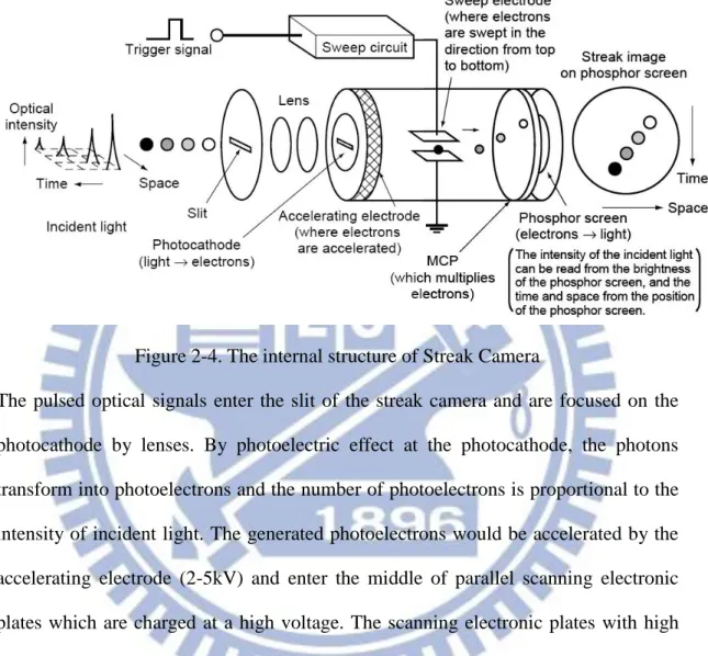
2.3.2 Streak Camera
Streak Camera detects the electronic signals which are proportional to the photoelectrons generated on the photocathode by photoelectric effect.
Figure 2-4. The internal structure of Streak Camera
The pulsed optical signals enter the slit of the streak camera and are focused on the photocathode by lenses. By photoelectric effect at the photocathode, the photons transform into photoelectrons and the number of photoelectrons is proportional to the intensity of incident light. The generated photoelectrons would be accelerated by the accelerating electrode (2-5kV) and enter the middle of parallel scanning electronic plates which are charged at a high voltage. The scanning electronic plates with high voltage will shift the direction of electrons with time and the swept electrons go into the multi-channel-plate (MCP). Photoelectrons will be enhanced by thousands of times when passing through the MCP and hit the screen with fluorescent agent, at which they would be transformed into the optical signals. The horizontal axis represents space axis and the vertical axis represents time axis on the screen. The resolution of the streak camera depends on the scan rate and then higher resolution needs fast scan rate which depends on the electronic system. Although the streak camera can get the all spectrum, it cannot detect the find structure.
10
2.4 Upconvesion Spectroscopy Using Sum-frequency
Generation
[7, 8]2.4.1 Sum-frequency Generation
In nonlinear optical media, the Maxwell’s equations can be written in Gaussian unit form.
In free space, there is no free charge ( ) and free currents ( ). We assume that the materials are nonmagnetic ( ). In nonlinear optical materials, the relation between and is
The polarization vector and the displacement field can be decomposed into linear and nonlinear term.
The separation of the linear part of the polarization vector and the displacement field is given by
11
Take curl of the Faraday’s law and replace by to obtain the equation
By extending the displacement field into linear and nonlinear term, the wave equation becomes
Consider the case of a lossless, dispersionless medium. The relation between and can be presented in term of a real frequency-independent dielectric tensor . For isotropic materials, the from tensor would be changed into scalar then it can simplify the equation.
(anisotropic) (isotropic) Eq. (12)
For the case of an isotropic material, the wave equation becomes
This equation has the form of driven (i.e., inhomogeneous) wave equation; the nonlinear response of the medium acts as a source term which appears on the right-hand side of this equation. This wave equation admits solutions of the term of free wave propagation with the velocity , where n = [] 1/2 is the linear index of refraction. By using an identity form vector calculus, the first term on the left-hand side can be written as
12
The wave equation in nonlinear optical medium can be simplified to the form
In nonlinear optics, the nonlinear optical response can be written by the polarization as a power series in the field strength as
It shall refer to as the second-order nonlinear polarization and to as the third-order nonlinear polarization. Two different frequencies incident to the nonlinear optical medium can be characterized by a nonlinear susceptibility . The field can be express as
The second-order contribution to the nonlinear polarization can be written
13
c.c.+2 2E1E1 +E2E2 Eq. (19)
The distinct amplitude of various frequency components of was defined as second-harmonic generation (SHG), sum-frequency generation (SFG), differential-frequency generation (DFG), and optical rectification (OR).
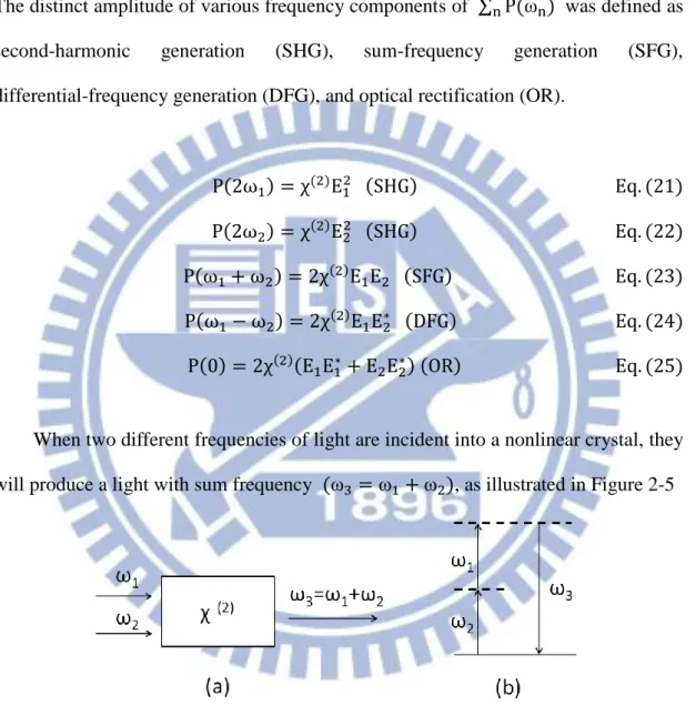
When two different frequencies of light are incident into a nonlinear crystal, they will produce a light with sum frequency , as illustrated in Figure 2-5
Figure 2-5. (a) Sum-frequency generation. (b) Photon description of the interaction of three optical waves.
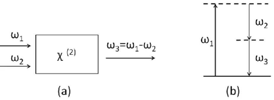
For different-frequency generation, incident optical signals with two different frequencies will produce a light, the frequency of which is = , as illustrated in Figure 2-6.
14
Figure 2-6. (a) Difference-frequency generation. (b) Photon description of the interaction of three optical waves.
2.4.2 Phase Matching Angle
To get the nonlinear optical effect with high conversion efficiency, we need to choose the particular incident angle of the nonlinear crystal satisfying phase-matching condition. For sum-frequency generation, the intensity of the generated field at frequency varies with the wave vector mismatch
According to
It shows that the sum-frequency efficiency decreases dramatically when the phase matching condition, , is not satisfied. The conditions for perfect phase matching with collinear beams are,
15
It is possible to achieve the phase matching condition by making use of anomalous dispersion and for this we can use the birefringent materials. The refractive index of birefringent materials depends on the direction of polarization of the optical radiation in birefringence.
Midwinter and Warner (1965) defined the type Ⅰ phase matching where the lower-frequency waves have the same polarization , and type Ⅱ to be the case where the polarizations are orthogonal, as illustrated in Table 2-1.[10]
Table 2-1. Two Phase-matching types for uniaxial crystals
We can make a mathematical derivation to get the phase-matching angle in nonlinear crystal. We consider the case of collinear phase-matching and then the condition for perfect phase matching reduces to
If the x, y, and z are the principal dielectric axes and nx, ny, nz are the indices of refraction for waves polarized along these directions, for the wave propagation along the direction k in the inset of Figure 2-7, the index ni at energy i satisfies
16
It only considers uniaxial crystal for which the optic axis along the z direction and (ordinary index), (extraordinary index) and then the equation can be rewrite by the expression.
It can also be rewritten as
The refraction index with different wavelength can be expressed in the form of Sellmeier’s equation
In our experiment, we use TypeⅠphase matching condition : . The phase-matching angle θ is given by
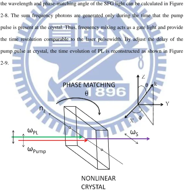
17 It can generate sum frequency wave when the crystal is rotated to the phase-matching angle θ as shown in Figure 2-7. If the PL light is in a different wavelength range, the wavelength and phase-matching angle of the SFG light can be calculated in Figure 2-8. The sum frequency photons are generated only during the time that the pump pulse is present at the crystal. Thus, frequency mixing acts as a gate light and provide the time resolution comparable to the laser pulsewidth. By adjust the delay of the pump pulse at crystal, the time evolution of PL is reconstructed as shown in Figure 2-9.
Figure 2-7. Sum frequency radiation of type I is generated in a nonlinear crystal. The inset defines the angles θ and φ.
18
Figure 2-8. The theoretical calculation of SFG wavelength and the phase-matching angle, where PL is in the range of wavelength from 380nm to 900nm.
19
For simplicity, the phase matching angle which calculated before is in the collinear case. However, In order to easily discriminate the SFG signal from other lights, the system setup is in the noncollinear case as shown in Figure 2-1. The sum-frequency efficiency decreases dramatically when the phase matching condition which extended to 3-D is not satisfied. For a finite crystal length L and a Gaussian transverse pump intensity profile of finite width W, SFG is possible to occur even , that is, with imperfect phase-matching.
The function is a weighting function for the intensity of the emitted downconversion that has a maximum value of 1 for , and falls to zero as the phase mismatch increase. For the noncollinear phase-matching shown in Figure 2-1, the phase-matching condition is satisfied with
Where
The equation can be rewritten as:
The phase-matching angle θ form Eq. (36) can be rewritten. Where the is given by Eq. (46).
20 θ By solving the equations, the retracing behaviors of the phase matching angle in non-collinear case can be numerically calculated.[12] When and increases, the phase matching angle shifts to a large value.
Figure 2-10. The view of crystal and laboratory frame coordinates, showing a typical arrangement for upconversion in a noncollinear case within a crystal.
21
2.4.3 Quantum Efficiency of Upconversion
Under the condition that only a small fraction of the power at is transferred to (negligible pump depletion), the quantum efficiency is given by
Here, is the pump beam, is the area of beam overlap with PL beam at the nonlinear crystal, is the effective nonlinear coefficient of the crystal, c is the velocity of light, is the free-space permittivity, and is the thickness of nonlinear crystal.
Crystal Lithium Iodate
LiIO3[13] BBO[14] Index λ in μm Transparency Range (μm) 0.3-5.5 0.19-3.5 deff strongest
22
In type I phase-matching condition, the of BBO can be calculated from Table2-2.
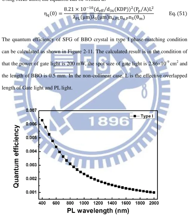
Using MKS units, the equation can be written as
The quantum efficiency of SFG of BBO crystal in type I phase-matching condition can be calculated as shown in Figure 2-11. The calculated result is in the condition of that the power of gate light is 200 mW, the spot size of gate light is 2.86×10⁻⁹ cm2 and the length of BBO is 0.5 mm. In the non-collinear case, L is the effective overlapped length of Gate light and PL light.
Figure 2-11. The quantum efficiency of SFG in type I phase-matching condition in the PL wavelength range from 400 nm to 2000 nm.
23
2.5 Design of Upconversion Luminescence System
2.5.1 Optical Setup
In this work, we use the Chameleon Ultra laser system, which delivers femtosecond pulses at an 82 MHz repetition rate with pulses width 120 fs, with a average power up to 3.6W at 800nm.
Figure 2-12. (a)Femtosecond pulses output at 82Mhz repetition rate and pulse width 120fs. (b)The chameleon laser head
In our up-conversion system as shown in Figure 2-13, the laser output beam of 800nm goes into the nonlinear crystal BBO to produce second harmonic generation and then the fundamental pulses at 800nm and the SHG signals at 400nm are separated by a dichronic mirror. The transmitted beam of 800nm goes through the time-delay stage to control the optical path difference and a half-wave plate to adjust the polarization. Finally, the light of 800 nm is focused on the second BBO crystal. The light of 400nm is used to photoexcite the sample. The sample is placed in the vacuum chamber which is connected to a closed-loop liquid helium cooling system as is shown in Chap. 3. The photoluminescence is collected and collimated by a lens. The collimated PL light is transmitted to the dichronic mirror and focused on the BBO crystal.
24
Figure 2-13. Schematic experimental arrangement for up conversion spectroscopy
In order to get sum-frequency generation, we needed to ensure that (1) two focused beam are overlapped, (2) the optical path differences of two light are zero and (3) the BBO is rotated to the phase-matching angle. If these three points are under control, we can get better SFG signals. The generated SFG signals pass through an aperture and a color filter to filter the scattered light of 800nm and 400nm. The optical fiber was used to deliver the signal to the monochromator to select the accurate wavelength in an accuracy of 0.01nm. The detector we used was Hamamatsu photomultiplier tube (PMT) R4632 with amplifier. The PMT transforms the photonic signal into electronic signal and delivers the electronic signal to the photon counter SR400. By using the single photon counting technique with a PMT and photon counter SR400, we could get high signal-to-noise ratio time-resolved spectrum.
25
2.5.2 Single Photon Counting Technique
[15, 16]Single photon counting technique is a powerful technique to highly enhanced signal-to-noise ratio in an extremely low signal. It consists of a PMT and a photon counter. We will make a description of the structure of PMT, and show how the photon counter worked in this part.
(I)PMT
A PMT consists of a photocathode, an electron multiplier (composed of several dynodes) and anode as shown in figure 2-14. When the light enters the photocathode of PMT tube, the photocathode generates photoelectrons. A photoelectron will be multiplied when pass through many dynodes. The photoelectron forms an electronic pulse from the anode.
Figure 2-14. Photomultiplier tubes operation in single photoelectron state[16]
Photomultiplier tubes (PMT), photodiodes, CCD image sensor are widely used in low-light-level detection. These detectors collect the light and output analogs electrical signal (current or voltage) in most application. When the light level becomes so weak that only a few photons are collected and the incident photons are
26
detected as separate pulses, we use single photon counting method which is also referred to as digital mode. Because of the operating characteristic of PMT tubes, single photon counting method has better stability, efficiency and signal-to-noise ratio than analogs signals measurement as illustrated in Figure 2-15.
Figure 2-15. The signals of PMT tubes generated and output in higher light level and lower light level. [16]
(II) Photon Counter
The output electronic pulses are sent to the preamplifier to enhance its voltage and then sent into the photon counter SR400. There are build-in discriminator, pulse shaper and counter in the SR400 as illustrated in Figure 2-16. We set the discriminate level in the interval between the pulse voltage and background. The passable pulse
27
goes into the pulse shaper and becomes the TTL signal. The counter can count the number of TTL signal. We can select an appropriate voltage to get the undistorted spectrum and open the gate in a long time interval to enhance the signal-to-noise ratio.
Figure 2-16. Typical photon counting system
2.5.3 Data Acquisition by LabView
In order to make a practical measurement, it needs to use automatic control in our measurement. The translation stage, rotation stage and photon counter should be controlled by LabView program. The flow chart of the program is shown in Figure 2-17. At first, we set the origin point of the stage and then the stage started to move. The stage moves one step and the gate of photon counter opens in a time interval depending on T. Finally, the gate is closed in a time interval depending on dwell and finishes one period. After N periods, the data is saved. However, the control of the stage and photon counter is not synchronous, so it needs to consider the correlation of time, as shown in Figure 2-18, to make the periodical measurement. Figure 2-19 is the front panel of the upconversion program. All the control of stage and photon counter can be done in this interface.
28
Figure 2-17. The flow chart showed how the program worked in a whole scanning process
Figure 3-18. The timing diagram illustrated how photon counter and stage worked in a period.
29
Fig. 2-19 The labview front panel that used in the automatically control of upconversion system.
①The channel of CH1:T or CH2:R is used to switch the control in translation stage or rotation stage.
② The stage control panel
Scanning step:Selecting the step in a whole measurement.
Pulse/step :Enter the numbers of pulses in one step. In the translation stage, the pulse is mathematically converted into μm (1μm = 20 pulses) while the pulse is converted into degree (1 deg = 400 pulses) in the rotation stage.
30
original position is also converted into μm or degree in the mathematical relationship as mentioned above.
③ The photon counter control panel
Dwell time:It controlled the time that the gate was closed. We set the dell time in the minimum of 2 msec.
Input level (V):This is the control of discrimination level in a range of -300 mV to 300 meV.
# of measurement:In the photon counting mode of CW that we used, we set the value of 1.
T set: This is the control of the time interval that gate opened. The time is depends on the trigger which we use the internal trigger of 10 MHz. The T set is
mathematically converted into sec in the mathematical relationship of 1 sec = 107 set.
④These are the graphs of output spectrum when the whole scanning is finished. In the left, it is the translation stage graph where the x-axis is from optical path difference mathematically converted into time delay in the relationship of 1μm = 6.6 . In the left it is the rotation stage graph.
⑤The control of translation stage delay time. It needs to be set at the time of one period which is the summation of T set and dwell.
2.6 Theoretical Calculation of TRPL Signal Level
Because of the sensitivity of system is limited by the loss of optical component and the quantum efficiency of PMT, we need to know the level of signal intensity to select the appropriate optical component and a usable detector.
31
2.6.1 SFG Quantum Efficiency
First, the quantum efficiency of sum-frequency generation was calculated in our system. Use Eq. (45) and replace the variable by the system parameter and the optical parameter of BBO, as shown in Table 2-3, 2-4. All the parameters could be theoretically calculated in section 2.3 or measured in our system.
System Parameter Value
Gate light area
PL light area
Gate light power
PL light power
BBO length
Table 2-3. The system parameter
Optical Parameter of BBO crystal Value μ μ @800 nm 1.660554 @800 nm 1.660554 @400 nm 29.19 deg 1.660553 3.948937
Table 2-4. The Optical parameter of BBO crystal
The theoretical quantum efficiency of sum-frequency generation in the system is calculated to be 0.7729%. Furthermore, the experimental quantum efficiency of sum-frequency generation was measured and compared to the theoretical result.
32
As shown in Figure 2-19, the power-dependent PL of SFG of 400 nm was measured with PL power from 200 μW to 0.1 μW. Using the parameter of detector cathode sensitivity, the output voltage can be converted into input power. By this way, the theoretical power-dependent PL intensity of SFG could be compared with the experimental value. We found that the actually measurement is five times smaller than the theoretical value as shown in Figure 2-20. The theoretical value of quantum efficiency of sum-frequency generation is needed to be corrected, multiplied by one fifth, in our system,
Figure 2-20. The power-dependent PL spectra of SFG of a wavelength 400nm generated from 800nm+800nm.
33
Figure 2-21. It is the Plots of the power of SFG versus the power of PL.
2.6.2 Power Loss by Optics
The system was separated into two parts by the position of BBO. All the transmissions of optical component obtained from the catalog as shown in Table 2-5 and the quantum efficiency of sum-frequency generation was calculated by Eq. (51) in section 2.3.3 and was corrected by multipling by one fifth. The InGaN nanorods with PL power of 40 nW with central wavelength 550nm was used as test sample. Finally, the signal intensity that entered into the PMT is measured to be 2.798 pW.
34
Element Focal Transmission QE Power(nW)
Sample 40 Ø 1" Silica lens 25.4mm 94.2%@550nm 37.68 Ø 2" Dichronic 98.0%@550nm 36.92 Ø 2" Silver mirror 96.0%@550nm 36.17 Ø 2"N-BK7 lens 100mm 90.1%@550nm 35.44 BBO 0.0954 % 0.0338 Ø 2"Silica lens 75mm 90.2%@326nm 0.0304 Ø 1"Silica lens 75mm 96.8%@326nm 0.0294 Color Filter 38.0%@326nm 0.0111 Grating 240/480mm 25.0%@326nm 0.00279 PMT
Table 2-5. The power lost by optical element.
2.6.3 Output Electronic Signal from PMT
We use the Hamamtsu PMT R4632 for extremely low light level detection. The specification from the Hamamatsu website is listed in Table 2-6.
Parameter Value
Collection Efficiency(side-on) 60%
Quantum efficiency@326nm
Gain@1000V
Dark Counts@ 50 s-1
Anode Pulse Rise Time 2.2 ns
Table 2-6. The character of PMT R4632
One photon can generate one electron from the photocathode in the ideal condition. In the real case, however, it depends on the collection efficiency and quantum efficiency of PMT. With the light of 32.1 pW of 326nm, the number of photon (Np) is
35
The output number of electronic pulse ( ) from PMT is
Where QE is the quantum efficiency@326nm and is the collection efficiency of side-on type. We got a theoretical calculation the number of PMT output electronic pulses. The output signal level is high enough to the dark counts at 25 of 50 s-1 counts.
2.6.4 Photon Counter Discrimination Level.
The characteristics of the single electronic pulse can also be calculated. In the photon counting mode, a single photoelectron is emitted from the photocathode with . The gain μ of PMT tube is . The charge of output electronic pulse is
The pulse width of the output signal is 2.2ns, so we can get the output pulse peak current
36
The input impedance of amplifier is 50 and the output peak voltage becomes
If set the discrimination level at the range about 12.7 mV, it can get the better signal-to-noise ratio for single photon counting technique.
2.7 Test and Improvement
In order to get the SFG of InGaN PL, we first used 800nm+800nm to find the visible SFG of 400nm and then changed to 800nm+400nm to find the SFG of 266nm in the UV range. Finally, change to 800nm+550nm to find the SFG of 326nm. For every change of different wavelength, we ensured that the optical path of pair of lights would be fixed and checked the three parameters we mentioned in the section 2.5.2, overlapping, optical path difference and phase-matching angle, are in the accurate vales.
2.7.1 Angular Resolution
The motorized rotation stage could scan the angular-dependence PL of SFG of 400mm. Figure 2-22 is the profile with the angular-dependence semi-logarithmic PL spectra. The linear scale PL spectra and the FWHM are shown in the inset with the value 0.27 degree. It means that the phase matching angle needs to be adjusted in an accuracy of 0.13 degree. Our motorized rotation stage can rotate in an accuracy of 0.01degree.
37
Figure 2-22. The angular-dependent semi-logarithmic-scale PL spectrum of SFG of 400nm. The inset spectrum on a linear scale showed the FWHM of 0.27degree.
2.7.2 Photon Counter Test
The SFG of 266nm was used to test the Photon Counter. The pump light was fixed at 400 nm in a power of 40 nW. Using the photodiode detector to measure the cross-correlation signal as shown in Figure 2-23, we could fit the spectra by gauss function and got the pulse width of 228 fs, which is greater than the laser pulse width 120 fs. The broadened pulse width may be due to the dispersion of optical lens or the low signal-to-noise ratio of photodiode. The photon counter integrates the counts by opening the gate in a different time interval and all the measurement was fixed at the discrimination level of 31meV as shown in Figure 2-24. At the 0.3s integrated time, the spectrum was distorted because of the low signal-to-noise ratio in a short integrated time. At the 1s integrated time, the spectrum showed the better time-resolution with the pulse width 122 fs which is closed to the laser pulse width of
38
120 fs. The increase of integrated time resulting in the increase of signal-to-noise ratio, but is also reduced the time-resolution according to the broadened pulse width.
Figure 2-23. The spectrum is the time-resolved PL of SFG 266nm which measured by the photodiode detector.
40
Figure 2-24. The spectra of time-resolved PL of SFG of 266nm which measured by single photon counting technique. The counts integrated at 0.3, 1, 3 and 9 second that Showed different pulse widths and signal-to-noise ration.
41
In order to estimate the discrimination level of photon counter at 326nm, SFG of 266nm combined with the 400nm light of 40nW, which is in the level of InGaN PL of 550nm, was used. By selecting the proper discrimination voltage from 56 mV to 42 mV, the cross-correlation peak was increased with the decreased voltage and began to be caved when the voltage is below 48 mV, as shown in Figure 2-25. It is because the discrimination level is near the background level that the background signal was measured and the signal of 266nm was cut. Selecting the level at 50 mV, we could get the better signal-to-noise ratio and a pulse width of 139 fs as shown in Figure 2-26.
Figure 2-25. Cross-correlation signal of 266nm from discrimination level from 42 to 56 mV. The peak raise with the decrease of level from 56 mV to 50 mV and began caved at the level below 48 mV.
42
Figure 2-26. The spectrum of 266nm at the level of 50 mV showed better signal-to-noise ratio and the pulse width near the laser pulse.
2.7.3 Dispersion of Optical Lens
When the simulation light of 400nm change into the PL light of 550nm, it can’t promise that the optical path is unchanged. Because of the dispersion in optical lens, the spot size and the position of overlapping vary depending on the wavelength. The effect of dispersion could be numerically calculated by OSLO which is the lens design software. The back focal length versus wavelength of first and second lenses in our system was calculated by OSLO as shown in Figure2-27 and 2-28. The effect of dispersion is obvious in the lens with long focal length when the wavelength of simulated light was far from the wavelength of PL. In our experimental process, the wavelength from 400nm change to 550nm make a focal point move about 1 2mm. The movement of focal point could be compensated by adjust the translated stage of lens. We used a long working distance camera lens and a CCD camera with high sensitivity to monitor the spot to ensure that the two lights still overlap.
43
If we want to do upconvsersion of InN in NIR range in the future, we need to use the laser light of 800nm to simulate the light of PL of 1900nm. In this case, the effect of dispersion cannot be neglected and a parabolic mirror can replace the lens to remove the dispersion effect.
44
Figure 2-27. The numerical value of back focal length of the silica lens calculated by OSLO.
Figure 2-28. The numerical value of back focal length of the N-BK7 lens calculated by OSLO.
45
2.7.4 Reduce the Background Noise
In the real case, the power density of 400 nm from laser couldn’t directly represent the power density of 550nm from InGaN because of the 400nm is an ultrafast pulse and the PL of InGaN is a pulse with long time evolution. The system need to be more sensitive to the lower signal level. We need to ensure that the noise from the environment is filtered clearly and the noise from the electronic instrument inside the system is stable. The noise from the environment can be filtered clearly by the color filter, pinhole and monochromator. To reduce the electronic noise from the instrument, the PMT with low dark count is necessary as show in section 2.5.3. Using the oscilloscope to measure the output background level, we can find that the background of PMT output has an evidently sinusoidal oscillation due to the oscillation from the high power supply. To solve this problem, the Hamamtsue DAP-Type socket assemble with low ripple of 2 mV was selected to substitute the AD111 Photobyte-P™ Photomultiplier Detection System with high noise to enhance the sensitivity of the upconversion system.
46
Chaper 3 PL from InN Nanorods Arrays with a
Critical Size
3.1 Introduction
Indium nitride (InN) with a narrow direct band gap has superior electronic transport properties compared with other group-III nitrides so that InN has become attractive for various applications such as high-frequency electronic devices, near-infrared optoelectronics, and high-efficiency solar cells. In order to meet the request of the rapid down-sizing of electronic and photonic device dimensions, one-dimensional (1D) InN nanomaterials in the forms of nanowires (NWs), nanorods (NRs), and nanotubes (NTs) have been developed.[17-22] The high surface-to-volume ratio of 1D InN nanomaterials has also been proved to be beneficial in the enhancement of terahertz wave emission.[23] Several studies reported the results of photoluminescence (PL) of the InN films and its nanostructures.[24-28]Despite superior structural advantages, the observed photoluminescence (PL) from 1D InN is typically much weaker and its band is broader compared to the InN epilayers and the PL mechanism critically depends on the size of nanomaterials. In order to understand the size dependence of the thermal evolution of PL properties, we prepared a set of InN nanorods arrays with critical size and used the IR spectrometer to measure the temperature-dependent PL spectra.
In this chapter, we will introduce the basic PL theory, review the recently study in InN and finally make a whole temperature-dependent PL study in InN NRs of various rod size.
47
3.2 Background of Photoluminescence
[5, 29-31]Photoluminescence (PL) measurement is one of the useful optical methods to understand the material property. PL has been studied by large number of scientists as early as the late 19th century. By analysis the peak position, intensity and FWHM of PL spectrum, we can get invaluable information such as crystal quality, impurity, defect, thermal effect and band structure that may affect the material properties and the device performance in semiconductors. Luminescence in semiconductors is the phenomenon that involved electrons and holes. Electrons were excited from ground state to excited state by some energy from an external source, usually come from short-wavelength light, and leave a hole in the top of valence band. After an extremely short time (~100ps), electrons were relaxed from high energy level to the bottom of conduction band through carrier-carrier and carrier-phonon scattering to get thermodynamic equilibrium. Finally, the electrons were recombined with the hole. In the meantime, the excited energy is released as a light or thermal energy. The electron-hole pair from generated to be recombined through three processes.
1. Energy Absorption 2. Carrier Relaxation 3. Carrier Recombination
In this section, emphasis is placed on the radiative carrier recombination. When the carriers recombined, the energy released as a light or phonon. The light emitting process is called radiative recombination. There are four mainly radiative recombination processes as shown in Figure 3-1.
48
Figure 3-1. Four kinds of radiative recombination processes : (a) band-to-band recombination, (b) donor-accepter pair recombination (c) free and bound exciton recombination (d) free to bound recombination.
3.2.1Band-to-Band Luminescence
The transition process is attributed to the recombination of an electron in conduction band with a hole in the valence band. This carrier transition process has been observed in very pure crystal like Si, Ge and some Ⅲb-Ⅴb compounds at relatively high temperatures. At low temperature, the interaction of electron and hole is higher than thermal disturbance and then the luminescence is transfer into exciton luminescence.
3.2.2 Donor-Acceptor Pair Luminescence
49
between donor and acceptor. In the beginning of DAP recombination, the electron is located at the donor level and the hole is located at acceptor level. The initial energy state of DAP is
Where and are the energy of energy gap, donor state and acceptor state.When the recombination process is over, the electron is removed from the donor level, while in the donor level left an effective charge +1. When the hole was removed from the acceptor level also left an effective charge -1. The Coulomb force act on the donor and the acceptor, so the final energy state of DAP is
Where is dielectric constant for the static field, and r is the intrapair separation. The emission energy can be expressed as the function of .
When the was increased, the emission energy shifts toward lower energy. The in the crystal is discrete, so the spectra of DAP luminescence is composed of many sharp line.
3.2.3 Free and Bound Excitons Luminescence
An exciton is a composite particle made up of an excited electron and a hole interaction with each other. It moves in the crystal transporting energy and produces luminescence through the recombination of an electron and a hole. There are two kinds of excitons: the Wannier exciton and the Frenkel exciton. The Wannier exciton model is work well in Ⅲb-Ⅴb semiconductor. It is composed of an electron in conduction band and a hole in valence band. They are bonded together by Coulomb interaction. Wannier exciton can analogy to the hydrogen atom. The energy of an
50
exciton is given by
Where is the binding energy of the exciton. The binding energy with quantum number is like the energy state of hydrogen atom. It is given as
,
Where is the plank constant and μ is the reduced mass of the exciton given by μ . Although exciton can be looked like a hydrogen atom, there are radical differences in the mechanic of optical transitions. Hydrogen atom tended to exist in the ground state through released specific energy, but the released energy of the exciton involves in its generation and annihilation. The exciton travels in the crystal interacts with phonon, scattered by the defect, impurity center, and fluctuations by the chemical composition; therefore, the internal kinetic energy is changed. This leads to the broadening of luminescence band. If the exciton composed of the charge located at the donor level or acceptor level, it can’t travel in the crystal. The kinetic energy of translation is zero. This is called bond exciton. This radiation linewidth is less than free exciton and the ground level of a bond exciton is lower than the level of free exciton (n=1).
3.2.4 Free-to-Bound Luminescence
At higher temperatures, all the shallow impurities are ionized. The band-to-band transition is the main recombination process. At sufficiently low temperatures, the carriers are frozen on the impurities. We consider a p-type sample contain NA acceptors per volume. At low photoexcitation, the density of ne of free electrons in the
51
conduction band is less than NA. These free electrons can recombination with the hole trapped on the acceptors and release energy through radiation. This transition involving a free carrier and a charge bound to an impurity, is called free-to-bound transitions. The emitted photon energy in this case is given by Eg-EA, where EA is the shallow acceptor binding energy. The free-to-bound transitions is a simple way of measuring impurity binding energy.
3.3 Nonradiative Recombination
[32]The energy emitted in the form of heat in the semiconductor crystal lattice that due to the recombination of electron in the conduction band and a hole in the the valence band is called nonradiative recombination. On the whole, there are three ways of nonradiative recombination: defect recombination, surface state recombination, and Auger recombination. The defect and surface state recombination process were shown as Figure 3-2.
Figure 3-2. Nonradiative recombination processes : (a) defect recombination, (b)surface state recombination
Auger recombination include three particles:the energy released from an electron and hole which recombine in a band-to-band transition to another electron or hole. As illustrated in Figure 3-3, there was no energy released in a form of photon
52
when electron 1 recombines with hole 2. Instead of the photon was emitted, the energy transfer energy to carrier 3 to position 4. In the way of clash, it will observe the conservation law of energy and momentum.
Figure 3-3. The process of Auger recombination. C, H, L, S, is conduction band, heavy hole band, light hole band, and split-off band, respectively.
3.4 Recent Researches in InN Nanorods and InN Epilayer
3.4.1 Electron Accumulation Layers of InN film
[33, 34]Recently, the surface accumulation layers in InN film have been studied. In a fully relaxed and uniform quality InN film, the sheet carrier density increased linearly with film thickness, which means there is a constant carrier density throughout the bulk InN. However, the sheet carrier density was nonzero when the thickness of InN approached to zero. It is means that the carriers are not uniformly distributed in the InN film. By study metal/InN contact and the C-V measurements, it is determined that the residual sheet charge should composed of surface sheet charge and interface sheet charge. An intrinsic surface electron accumulation layer was measured by investigated
53
the electronic structure of clean InN (0001) surface by a high resolution electron-energy-loss spectroscopy of the conduction band electron plasmon excitations. The observed electron accumulation at the surface of n-type InN is due to the presence of positively charged donor-type surface state. Charge-profile calculation reveals a surface state density of , which gives rise to a band bending of 0.56 eV to maintain charge neutrality, thus locating the Fermi-level 1.64 eV above the valence band maximum.
3.4.2 Carrier Localization of InN Film
[35-37]The radiative and nonradiative recombination process in lnN film has studied. The nonradiative recombination rate were thermally activated could be expressed as the equation
Where is activation energy and is boltzmann constant. On the steady state, the PL Intensity is proportional to τ . We can obtain the familiar expression of PL intensity
If there are two competitive nonradiative recombination channels, the equation can be rewrite as
. Where and are the activation energies at low and high temperature, respectively, related with the thermal quenching and is the Boltzmann’s constant, and and C1 and C2 are fitting constant.
The activation energy by the Eq. (64) is 7.8meV. The peak energy of lnN film shown the s-shift because of the excitons localization phenomena and found the localization energy is 14meV. Using the ratio between radiative lifetime and the
54
localization energy at a small variation could roughly get the localization energy of of 30meV. This value is twice the value of 14 meV. The activation (7.8 meV) that ruled the nonradiative recombination channels is too small for compete the localization energy. The discrepancy would due to underestimate the material parameter which used in the mathematical description in localization energy.
The concentration dependence of carrier localization in InN epilayers has also been discussed. The PL intensity of InN as a function of temperature could be successfully fitted by the two channels Eq. . could be extracted at the high temperature regions (above 100) and at low temperature (10-100 K). The activation energy is 30meV, and the activation energy is depends on the carrier concentration. The localization energy is the function of carrier concentration. It is 4.5meV when the carrier concentration is about . The activation energy is closed to the value of localization energy. They suggested that is caused by the nonradiative channel through defect or dislocations in InN and is due to the thermalization processes that make the carriers from localized state change into delocalized.
3.4.3 Anomalous Optical Property in InN Nanorods
[25, 27]The temperature-dependent near-infrared photoluminescence of InN nanorods compared with the InN film has been discussed. The naonorods of uniform diameter of 130nm showed slight blueshift and significantly broaden bandwidths when increasing temperature from 12-300 K. Compared with the nanorods of uniform diameter of 130nm, the peak positions of nanorods of mean diameter of ~130nm, ~60nm showed no shift with increasing temperature while the PL peak shift of InN epilayer followed a normal trend. The PL phenomena were largely because of intrinsic electron accumulation at the surface on n-type lnN. The considerable band bending
55
due to the surface accumulation layer has been established. It results in an inhomogeneous spatial distribution of the degenerate electron concentration, and it can generate the anomalous shift and broadening of PL. At low temperature, the photoholes are distributed over the inner of core where is remote from the electron accumulation layer. The increasing in temperature leads to the distribution of photoholes over broader region inside the nanorods, where the hole potential energy is in the order of thermal energy KBT. With a strongly inhomogeneous electron distribution, the phenomena can overcome the trend of band gap shrinkage and results in the anomalous blueshift. Due to the structurally less perfect InN nonorod of 130nm diameter contain more valence band tail state, these unusual temperature effects are most pronounced.
3.5 Sample and Experimental Setup
In our experiment, All InN nanorods and film were performed by Y.-L. Hong in Prof. S. Gwo’s lab in National Tsing Hua University.
3.5.1 InN film
A wurtziteN-polar (c-axis) undoped indium nitride (InN) film was grown on Si(111) substrates at 520 by plasma-assisted molecular beam (PAMBE) using the epitaxil AlN/β-Si3N4 double-buffer layer technique, as show Figure 3-4. From the scanning electron microscope (SEM), as shown in Figure 3-5, we can know that the film thickness of the sample is 1μ . The electron concentration of InN Film is by room-temperature Hall Effect measurements.
56
Figure 3-4. InN film was grown on Si (111) substrates and use the epitaxial AlN/β-Si3N4 double-buffer layer technique.


![Figure 1-1. The energy bandgaps of III-Nitride group semiconductors . [2]](https://thumb-ap.123doks.com/thumbv2/9libinfo/7980522.159023/13.892.131.763.410.1071/figure-energy-bandgaps-iii-nitride-group-semiconductors.webp)