Selective Growth of Carbon Nanotubes on Prepatterned
Amorphous Silicon Thin Films by Electroless Plating Ni
C. W. Chao,
*
,zYewChung Sermon Wu, Gau-Ren Hu,*
and Ming-Shian FengDepartment of Materials Science and Engineering, National Chiao Tung University, Hsinchu 300, Taiwan, China
Selective growth of carbon nanotubes共CNTs兲 synthesized at low temperature by electroless plating Ni was proposed for the first time in this study. After electroless plating, Ni nanoparticles were selectively deposited on the prepatterned amorphous silicon 共a-Si兲 thin films. After plasma-enhanced chemical vapor deposition, well-aligned CNTs were observed only on the Ni-coated a-Si islands. The diameter, density, and the field emission of CNTs could be controlled easily by the Ni plating time. The achievement of controlling the site density and growth area is significant for applications of carbon nanotubes as field emission devices, nanoelectrode arrays, etc.
© 2003 The Electrochemical Society. 关DOI: 10.1149/1.1596953兴 All rights reserved.
Manuscript submitted September 23, 2002; revised manuscript received March 12, 2003. Available electronically July 30, 2003.
Carbon nanotubes共CNTs兲 have attracted extensive attention due to their unique physical properties and applications.1-5 One of the most attractive applications of CNTs is the electron emitter for field emission displays because CNTs have a low field emission voltage and a large current density.6-8For field emission displays, the sub-strates are usually made of glass substrate because of its low price and good vacuum sealing. Therefore the growth temperature of CNTs for field emission displays must be lower than glass strain temperature共600°C兲.
Intensive studies have been done to lower the synthesis tempera-ture of CNTs.9-12Metal catalyst is one of these efforts, in which Ni, Fe, and Co are used either separately or together as composite catalysts.6-15 When CNTs were synthesized with low temperature, the size of metal catalysts needs as small as possible because the size of metal catalysts must be smaller than the diffusion length of carbon,16which increased with the temperature.
The diameter and the site density of CNTs can be controlled by changing the particle size and the site density of catalysts.15,17The density of catalysts can be controlled by lithography,18,19 micro-contact printing,20shadow mask,4etc. However, all these methods either require expensive equipment and intensive labor or cannot control the site density in large area.15In order to control the site density of the catalysts, Tu et al. used the pulse-current electro-chemical deposition technique to prepare Ni nanoparticles.15 The experiment was carried out on a two-electrode system. The working electrode was prepared by sputtering a layer of Cr on a silicon wafer to get a conductive surface. The nucleation site density of the Ni nanoparticles was controlled by changing the magnitude and dura-tion of the pulse current. After plasma enhanced共PE兲 hot filament chemical vapor deposition 共CVD兲, the site density of the aligned CNTs varied from 105to 108cm⫺2.
In addition to the site density of CNTs, the selective growth of CNTs is another important issue for the application of field emission displays. In a previous study, Chen et al.14 proposed a new field emission device composed of carbon nanotubes and a thin film tran-sistor 共TFT兲, in which iron film was selectively deposited on the drain area of poly-Si TFT which was followed by synthesis of the CNTs on the drain area. They found that the emission stability has been significantly improved.
In this study, a similar electrochemical deposition technique as described in Ref. 21 was used. An electroless plating Ni method was introduced to control the growth of Ni nanoparticles. During the plating process, Ni nanopartilces were deposited by a redox reac-tion. Since there was no external current and voltage involved, no conductive electrode layer was required. To control the deposition of
the Ni nanoparticles, a-Si films were patterned by photolithography before plating. After the PECVD process, CNTs were found to grow selectively on the a-Si islands.
Experimental
The substrates used in this study were 1⫻ 1 cm silicon 共100兲 chips with 500 nm thick SiO2films, which simulated the glass sub-strate. Amorphous silicon共a-Si兲 films with a thickness of 100 nm were then deposited by a low-pressure CVD 共LPCVD兲 system at 550°C. Amorphous Si islands were defined by photolithography and etched by reactive ion etching 共RIE兲 method. The samples were cleaned with a solution of H2SO4 and H2O2. After being dipped into the diluted HF solution to remove the native oxide on the samples, the samples were dipped into the plating solution for 60, 90, or 120 s to coat Ni nanoparticles. The composition of plating solution was NiCl2•6H2O 30 g L⫺1, NH4Cl 50 g L⫺1, NaH2PO3 H2O 10 g L⫺1, and C6H5Na3O7H2O 84 g L⫺1.21The plating tem-perature was kept at 80°C and the PH value of the plating solution was 8.0.
After electroless plating, the substrates with Ni nanoparticles were loaded into a PECVD chamber, where CNT growth was per-formed. Before the growth of CNTs, H2gas was introduced into the chamber to activate the surface of Ni nanoparticles for 10 min The pressure of reaction was 20 Torr and the flow rate of H2 was 80 standard cubic centimeter per minute 共sccm兲. The microwave plasma input power was 1000 W and the substrate temperature was 580°C. To grow the CNTs, a mixture of methane and hydrogen gases was then admitted to the chamber. The flow rates of methane and hydrogen were 4 and 80 sccm, and the negative bias of substrate was⫺100 V.
Field emission measurements were carried out on these samples using the apparatus shown in Fig. 1. The anode electrode was placed 100m away from the substrate. The size of measured field emit-ting area was 5 mm2.
*Electrochemical Society Student Member.
zE-mail: [email protected] Figure 1. Schematic diagram of the field emission measurement apparatus.
Journal of The Electrochemical Society, 150共9兲 C631-C634 共2003兲
0013-4651/2003/150共9兲/C631/4/$7.00 © The Electrochemical Society, Inc.
C631
) unless CC License in place (see abstract). ecsdl.org/site/terms_use
address. Redistribution subject to ECS terms of use (see 140.113.38.11
Results and Discussion
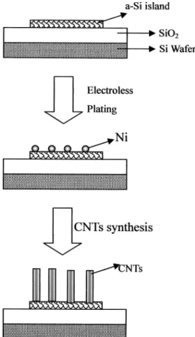
The scanning electron microscope共SEM兲 images of Ni nanopar-ticles with various lengths of plating time are shown in Fig. 2. Re-gardless of the plating time共60-120 s兲, no Ni cluster was found on the oxide area. The Ni nanoparticles were only selectively deposited on the a-Si islands. When the plating time was 60 s, the typical diameter of Ni nanoparticles was about 20 nm and the density of Ni nanoparticles was 7⫻ 107/cm2. As shown in Fig. 2 and Table I, the density and the size of Ni nanoparticles increased monolithically with the plating time, as expected. When the plating time increased to 120 s, the diameter of Ni nanoparticles reached 150 nm and the density reached 1⫻ 1010/cm2. Figure 3a shows the typical SEM images of samples after the growth of CNTs. The light features seen in the micrographs correspond to CNTs grown on the top of a-Si islands. CNTs were only selectively synthesized on the Ni-coated a-Si islands. No CNT was found on the oxide surface. The nature of the well-aligned CNTs was verified using SEM as shown in Fig. 3b. The advantages of Ni catalysts prepared by electroless plating are illustrated in Fig. 4. The Ni catalysts were only deposited on the a-Si island but not on the oxide surface. Therefore, during low tempera-ture CNT synthesis, CNTs could be selectively synthesized on the a-Si pattern without using the lithograph process.
When the plating time was 60 s, the diameter of the bottom of CNTs was 45 nm, while the diameter of the top of CNTs was only 20 nm. These carbon nanotips were formed because CNTs were anisotropically etched by hydrogen plasma.22-24It is believed that during the growth of CNTs, the active carbon species in the plasma are accelerated to the substrate by the negative bias to form the
Figure 2. SEM images of Ni nanoparticles on the a-Si patterns after
elec-troless Ni plating for共a兲 60 s, 共b兲 90 s, and 共c兲 120 s.
Figure 3. 共a兲 SEM image of CNTs selectively synthesized on the a-Si
pat-terns, and共b兲 high resolution SEM image of these vertical aligned CNTs.
Table I. Effects of Ni plating time on the site density and diam-eter of Ni nanoparticles, and the diamdiam-eter of CNTs.
Ni plating time 共s兲 Density of Ni nanoparticles 共particle/cm2兲 Diameter of Ni nanoparticles 共nm兲 Diameter of CNTs 共nm兲 60 7 ⫻ 107 20-30 20-45 90 2 ⫻ 109 40-80 60-80 120 1 ⫻ 1010 30-150 75-200
Journal of The Electrochemical Society, 150共9兲 C631-C634 共2003兲
C632
) unless CC License in place (see abstract). ecsdl.org/site/terms_use
address. Redistribution subject to ECS terms of use (see 140.113.38.11
CNTs. Meanwhile, the accelerated active hydrogen radicals etch the top of CNTs and form the carbon nanotips.23Fortunately, the for-mation of these nanotips could enhance the field emission of CNTs.24
It was also found that the density of CNTs increased with the Ni plating time, as shown in Fig. 5. This is due to that CNTs were induced by Ni particles. As shown in Fig. 1 and Table I, the density of Ni particles increased with the plating time; therefore, the density of CNTs increased. Figure 5 and Table I also indicate that the diam-eter of CNTs increased with the plating time. In other words, the larger the Ni nanoparticles, the larger the CNTs. This result is con-sistent with the conclusion drawn by Ref. 15 and 17, during their CNT growth studies. They found that larger catalyst particles pro-duced larger CNTs. As shown in Fig. 4, the diameters of the top of CNTs were also found to be sharpened by the anisotropically hydro-gen plasma etching, regardless of the Ni plating time. Fortunately, this reduction of the CNTs diameter could enhance the field emis-sion of CNTs.
The field emission current of CNTs versus applied electric field is shown in Fig. 6. The threshold field, which was defined as the current densities reached 1A cm⫺2, was significantly affected by the Ni plating time. When the Ni plating time was 60 s, the threshold field was 4.5 V/m where the current started to increase exponen-tially with electric field. When the plating time increased to 90 s, the threshold field decreased to 3.5 V/m. With further increase of the plating time to 120 s, the threshold field, however, did not decrease but increased to 4.0 V/m.
Two factors can affect the threshold field共field emission current兲: the radius共diameter兲 of CNTs and density of CNTs. The effect of the radius on the field emission current can be deduced from the Fowler-Nordheim model.25,26In this model, the dependence of the emitted current I on the local electric field F and the work function⌽ is given by
I␣共F2/⌽兲exp共⫺B⌽3/2/F兲 关1兴
where B⫽ 6.83 ⫻ 109共V eV⫺3/2m⫺1兲. The local electric field F is not simply V/do, which is the macroscopic electric field obtained by applying a voltage V between two planar and parallel electrodes separated by a distance do. The local field is given by
F⫽ V/do 关2兴
where is determined by the shape of the emitter, and especially by its radius of curvature at the tip, ro. The basic approximation of is
Figure 4. The electroless plating processes for CNTs synthesis.
Figure 5. SEM images of CNTs on the a-Si patterns with electroless Ni
plating for共a兲 60 s, 共b兲 90 s, and 共c兲 120 s.
Journal of The Electrochemical Society, 150共9兲 C631-C634 共2003兲 C633
) unless CC License in place (see abstract). ecsdl.org/site/terms_use
address. Redistribution subject to ECS terms of use (see 140.113.38.11
 ⯝ d/共kro兲 关3兴 where k is a constant. Combining Eq. 1, 2, and 3, it is clear that both the local field F and emitted current I increased with decreasing radius of curvature. In other words, the threshold field increases with the diameters of CNTs.
Besides the diameter of the CNTs, the density of the CNTs also affects the threshold field. When the density of the CNTs increased, the distance between CNTs became shorter, which degraded the field emission of CNTs due to the screening effect.27,28
In this study, since the diameter increased with the Ni plating time, the threshold field of each CNT increased with the plating time. However, the density of CNTs increased significantly from 7 ⫻ 107
to 1⫻ 1010/cm2; therefore, the total emission current of CNTs still increased. In other words, the threshold field of CNTs decreased when the plating time increased from 60 to 90 s. With further increase of the plating time to 120 s, the diameter and den-sity of CNTs became too large. The threshold field of each CNT increased and the short distance between CNTs degraded the field emission of CNTs. Therefore, the threshold field increased to 4.0 V/m.
Conclusions
Selective growth of vertical aligned CNTs on the prepatterned amorphous silicon islands by electroless plating Ni has been ob-served for the first time in this study. The synthesis temperature of CNTs was as low as 580°C due to the Ni cluster catalyst. The di-ameter and density of Ni nanoparticles were found to increase with the Ni plating time. Since CNTs were induced by Ni nanoparticles, the density and diameter of CNTs could be easily controlled by the Ni plating time. Therefore, the field emission properties of CNTs could also be controlled by plating time. Using this selective growth
of vertical aligned CNTs, this simple process may be adequate for integration of CNTs into TFT on glass substrates, nanoelectrode arrays and other devices.
Acknowledgments
This research was supported in part by the National Science Council共NSC兲 of the Republic of China under grant NSC 91-2215-E009-046. Technical supports from the National Nano Device Labo-ratory of NSC and Semiconductor Research Center of National Chiao Tung University are also acknowledged.
National Chiao Tung University assisted in meeting the publication costs of this article.
References
1. R. Saito, M. Fujita, G. Dresselhaus, and M. S. Dresselhaus, Appl. Phys. Lett., 60, 2204共1992兲.
2. G. Che, B. B. Lakshmi, E. R. Fisher, and C. R. Martin, Nature (London), 398, 346 共1998兲.
3. A. C. Dillon, K. M. Jonse, T. A. Bekkedahl, C. H. Kiang, D. S. Bethune, and M. J. Heben, Nature (London), 386, 377共1997兲.
4. S. Fan, M. G. Chapline, N. R. Franklin, T. W. Tombler, A. M. Cassell, and H. Dai, Science, 283, 512共1999兲.
5. C. Zhou, J. Kong, and H. Dai, Appl. Phys. Lett., 76, 1597共2000兲. 6. W. A. deHeer, A. Chatelain, and D. Ugarte, Science, 270, 1179共1995兲. 7. W. Zhu, C. Bower, O. Zhou, G. Kochanski, and S. Jin, Appl. Phys. Lett., 75, 873
共1999兲.
8. K. A. Dean and B. R. Chalamala, Appl. Phys. Lett., 75, 3017共1999兲.
9. Z. F. Ren, Z. P. Huang, J. W. Xu, J. H. Wang, P. Bush, M. P. Siegal, and P. N. Provncio, Science, 282, 1105共1998兲.
10. J. H. Han, H. J. Kim, M. H. Yang, C. W. Yang, J. B. Yoo, C. Y. Park, Y. H. Song, and K. S. Nam, Mater. Sci. Rep., 16, 65共2001兲.
11. G. W. Ho, A. T. S. Wee, J. Lin, and W. C. Tjiu, Thin Solid Films, 388, 73共2001兲. 12. C. Klinke, J. M. Bonard, and K. Kern, Surf. Sci., 492, 191共2001兲.
13. J. Kim and K. No, J. Appl. Phys., 90, 2591共2001兲.
14. H. C. Cheng, W. K. Hong, F. G. Tarntair, K. J. Chen, J. B. Lin, K. H. Chen, and L. C. Chen, Electrochem. Solid-State Lett., 4, H5共2001兲.
15. Y. Tu, Z. P. Hung, D. Z. Wang, J. G. Wen, and Z. F. Ren, Appl. Phys. Lett., 80, 4018 共2002兲.
16. Y. Y. Wei, G. Eres, V. I. Merkulov, and D. H. Lowndes, Appl. Phys. Lett., 78, 1394 共2001兲.
17. Z. P. Hung, D. Z. Wang, J. G. Wen, M. Sennett, H. Gilbson, and Z. F. Ren, Appl. Phys. A: Mater. Sci. Process., 74, 387共2002兲.
18. Z. F. Ren, Z. P. Hung, D. Z. Wang, J. G. Wen, J. W. Xu, J. H. Wang, L. E. Calvet, J. Chen, J. F. Klemic, and M. A. Reed, Appl. Phys. Lett., 75, 1086共1999兲. 19. H. Murakami, M. Hirakawa, C. Tanaka, and H. Yamakawa, Appl. Phys. Lett., 76,
1776共2000兲.
20. L. Nilsson, O. Groening, C. Emmenegger, O. Kuettel, E. Schaller, L. Schlapbach, H. Kind, J. M. Bonard, and K. Kern, Appl. Phys. Lett., 76, 2071共2000兲. 21. A. Brenmer, Met. Finish., 11, 53共1954兲.
22. S. H. Tsai, C. W. Chao, C. L. Lee, and H. C. Shih, Appl. Phys. Lett., 74, 3462 共1999兲.
23. C. L. Tsai, C. F. Chen, and L. K. Wu, Appl. Phys. Lett., 81, 721共2002兲. 24. X. D. Bai, C. Y. Zhi, S. Liu, E. G. Wang, and Z. L. Wang, Solid State Commun.,
125, 185共2003兲.
25. J. M. Bonard, M. Croci, I. Arfaoui, O. Noury, D. Sarangi, and A. Chaˆtelain, Dia-mond Relat. Mater., 11, 763共2002兲.
26. J. M. Bonard, M. Croci, C. Klinke, R. Kurt, O. Noury, and N. Weiss, Carbon, 40, 1715共2002兲.
27. R. Kurt, J. M. Bonard, and A. Karimi, Thin Solid Films, 398, 193共2001兲. 28. K. B. K. Teo, M. Chhowalla, G. A. J. Amaratunga, W. I. Milne, G. Pirio, P.
Legagneux, F. Wyczisk, D. Pribat, and D. G. Hasko, Appl. Phys. Lett., 80, 2011 共2002兲.
Figure 6. Emission current vs. applied electric field curves.
Journal of The Electrochemical Society, 150共9兲 C631-C634 共2003兲
C634
) unless CC License in place (see abstract). ecsdl.org/site/terms_use
address. Redistribution subject to ECS terms of use (see 140.113.38.11