Ultra-low voltage implicit multiplexed
differential flip-flop with enhanced noise
immunity
W.-H. Sung, M.-C. Lee, C.-C. Chung and C.-Y. Lee
An ultra-low voltage 22T implicit multiplexed differential (IMD) flip-flop (FF) is proposed. An implicit multiplexer is designed to simplify the differential FF complexity, while its control data path is able to enhance the FF noise immunity as well. So, the fully static IMD-FF with modified differential topology provides a sufficient noise margin under voltage scaling. On the other hand, the IMD-FF oper-ation avoids considerable DC current dissipoper-ation to save active power and suppresses the idle leakage by stacked transistors. The post-layout simulation in 90 nm CMOS process with 400 mV supply voltage shows that the IMD-FF achieves 56% active power and 42.2% leakage power reduction. The tolerable noise energy is enhanced by 18.9% on average. Finally, this work provides 93% func-tion yield rate under the effect of process-voltage-temperature vari-ations and 40 pJ input noise energy.Introduction: The flip-flop (FF) is the most critical circuit in low energy VLSI systems. This is because FFs not only consume a large portion of system power and leakage, but also remain as the bottleneck in voltage scaling due to higher complexity than other logics. As supply voltage drops to near the sub-threshold region, the ratio between the
conduc-tance current IONand cutoff current IOFFis degraded in an exponential
order. ION is more difficult to charge and discharge internal nodes
against IOFFtowards the correct state. Such degradation is even worse
when considering the effect of process-voltage-temperature (PVT)
vari-ations, resulting in a poor static noise margin (SNM)[1]. That is, FFs
become quite sensitive to input noise induced from coupling crosstalk
or supply ripple[2].
To enhance the SNM for low voltage operation, FFs must maintain
sufficient driving ION and noise immunity at the same time. The
former can be achieved by removing dynamic logics or current conten-tion nodes, e.g. 2-INV positive feedback latch, from FF designs, while the latter normally depends on circuit topologies. The master-slave (MS) based FF is a well-known power and area efficient topology.
Especially, the clocked CMOS (C2MOS) FF[3]and transmission-gate
(TG) FF[4]are PVT insensitive owing to their static and complementary
design without a current contention node. However, MS-based FFs suffer weak immunity to noise appearing on the clock input since any induced noise pulse with merely short duration, i.e. a transmission-gate delay, might easily turn on the master/slave latch incorrectly. In
contrast, the static differential FF[5]requires higher noise energy to
drive the storage latch and related control signals, implying better noise immunity. Unfortunately, this structure occupies considerable
transistor counts and consumes more power. Note that, except [5],
most of differential FFs are unable to operate at low voltage because the commonly adopted NMOS shorting device (providing a ground path to avoid floating) fails to generate correct control signals with degraded current. Accordingly, an ultra-low voltage 22T implicit multi-plexed differential (IMD) FF is proposed for low energy operation. An implicit multiplexer (I-MUX) is designed to simplify the differential FF complexity, while its control data path is able to enhance noise immunity. The fully static IMD-FF with modified topology provides sufficient SNM under voltage scaling. In addition, the IMD-FF oper-ation avoids DC current dissipoper-ation to save active power, and its leakage current is reduced by stacked transistors.
Proposed design: Differential FFs contain the precharge unit and SR-latch. The precharge unit is applied to precharge and evaluate control signals S/SB (set) and R/RB (reset). The SR-latch determines output Q/QB according to S/SB and R/RB. For SB ¼ ‘0’ and RB ¼ ‘1’, Q will be set to high. For SB ¼ ‘1’ and RB ¼ ‘0’, Q will be reset to low. If SB and RB are both high, output Q will remain the same
logic. To solve the high complexity issue in[5]for power and area
reduction, the proposed IMD-FF utilises an implicit multiplexer
(I-MUX) to complete SR logics. Fig. 1a shows the I-MUX design
concept. From a truth table, the SR-latch function is realised by an equivalent 4-to-1 MUX simply. Then, the 4-to-1 MUX can be further translated to I-MUX, including an internal data latch constructed by INV1 and INV2. The differential N-MOS pass gates MN5 and MN6 are in charge of dual discharge path selection. For SB ¼ ‘0’ and
RB ¼ ‘1’, MN6 is turned on to discharge QB; for SB ¼ ‘1’ and RB ¼ ‘0’, MN5 is turned on to discharge QQ and Q. When SB ¼ ‘1’ and RB ¼ ‘1’, MN5 and MN6 are turned off for latch storage. Based on the operation of the I-MUX, the proposed IMD-FF circuit diagram
is shown in Fig. 1b. When CLK is low, SB/RB are precharged to
high, and then S/R are discharged to low. I-MUX (MN5 and MN6) is turned off to hold the data (QQ and QB) stored in MP1, MN1, MP2 and MN2, where SB/RB and S/R act as virtual VDD and virtual GND, respectively. When CLK is triggered to high, D (DB) will dis-charge SB (RB) to low through MN8 (MN7), and S (R) is dis-charged to high (low). Then, the I-MUX performs data path selection as indicated inFig. 1a. That is, when D ¼ ‘1’ (DB ¼ ‘1’), MN6 (MN5) is turned on to discharge QB (QQ), while QQ (QB) is charged by MP1 and MP3 (MP2 and MP4). QB QQ CLK DB SB CLK RB SB S R CLK D RB CLK Q MP5 MP3 MP4 MP6 MP7 MP1 MP2 MP8 MN1 MN2 MN 7 MN8 MN5 MN6 MN3 MN4 MN9 MN10 a b Q SB RB 0 0 0 0 1 1 1 1 X 1 0 Q RB SB QQ QB MN5 MN6 Q S R INV1 INV2 I-MUX RB SB 00 01 10 11 Q X
Fig. 1 Proposed IMD-FF design a I-MUX design concept b IMD-FF circuit diagram
Conventional differential FFs require an extra retention latch holding the ‘0’ logic of SB/RB in the evaluation phase to avoid floating until the next precharge of SB/RB, resulting in increased transistor counts. Instead, IMD-FF connects SB (RB) with data latch output QB (QQ) through MN4 and MN6 (MN3 and MN5) since QB (QQ) exists as a
dis-charge path to MN7 (MN8) as CLK ¼ ‘1’.Fig. 2shows the
implemen-tation of the SR-latch applied in a differential FF[5]and an IMD-FF,
excluding the precharge unit for simplicity. The IMD-FF occupies
14T to implement the SR-latch, while[5]contains 14T and 8T in the
data latch and the retention latch. Considering the precharge unit, the IMD-FF totally saves 14T. Besides, the operation of the IMD-FF pre-vents current contention to eliminate DC current dissipation because all charge and discharge paths of the SR-latch output QQ (QB) are con-trolled by MP3 and MN7 (MP4 and MN8) according to SB (RB). The I-MUX will not discharge QQ (QB) until SB (RB) turns off MP3 (MP4). On the other hand, as the I-MUX begins to discharge QQ (QB), QB (QQ) is being charged concurrently and its discharge path MN8 (MN7) has already been turned off by RB (SB). Moreover, most of the IMD-FF internal nodes are designed as a stacked structure to
min-imise VDSfor leakage suppression. For instance, RB, QQ, and S (SB,
QB, and R) are inserted between cascode transistors MP1, MN1, MN3, MN5, and MN9 (MP2, MN2, MN4, MN6, and MN10) since these nodes have the same logic value in the evaluation phase.
CLK=1 CLK=1 DB D RB SB SB SB RB RB R R S S SB RB S R CLKS CLKR QQ QB SR retention latch SR data latch Q Q SB RB conventional differential FF [5] MN5 MN9 MN3 S R MN6 MN10 MN4 retention path for SB=0 retention path for RB=0 proposed IMF-FF
Fig. 2 SR-latch implementation in[5]and IMD-FF
In the precharge phase, differential FFs provide better noise immunity than MS-based FFs since the noise pulse must retain sufficiently long duration to turn on the SR logics and lead the SR-latch to error state. However, differential FFs remain unstable in the evaluation phase since the noise pulse might easily enable the single gate delay precharge unit to erase the SR signals. Alternatively, to force IMD-FF function failure, the noise is required to turn on the precharge unit, SB/RB in-verter and the I-MUX successively, indicating the robustness of the IMD-FF for all conditions. Moreover, after noise pulse duration, the
I-MUX retention path is able to recover the SB/RB signal correctly to avoid an unknown state of SB/RB.
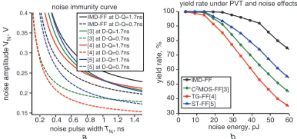
Experimental results: The IMD-FF and related designs are
implemented in 90 nm CMOS process, where the FF sizing is deter-mined by choosing minimal energy for a fixed D-to-Q delay. The
post-layout simulation inFig. 3shows the FF reliability analysis with
400 mV supply voltage and +10% variation.Fig. 3ais the noise
im-munity curve [2] which indicates the maximum tolerable noise
without function failure in terms of noise amplitude VN and pulse
width TN. When D-to-Q delay equals 0.7 ns, the IMD-FF improves
40.6% tolerable TN for VN¼ 0.2 V. Fig. 3b shows the FF function
yield rate under PVT and noise effects. Each point indicates the correct-ness probability from 20000 times of Monte-Carlo simulation with
varied process, temperature (0 – 1008C) and VTmismatch. The X-axis
represents input noise energy. The IMD-FF achieves 93% yield rate for 40 pJ input noise energy, but related designs decrease to below 80%. Table 1 lists the performance comparisons. Compared to [5], this work achieves 56% active power and 42.2% leakage power reduction. Besides, the index average noise threshold energy (ANTE)
[2]is enhanced by 18.9%, where the ANTE represents the average
toler-able noise energy of each curve inFig. 3a, i.e. E(VN2× TN), to
bench-mark noise immunity.
0 10 20 30 40 50 60 30 40 50 60 70 80 90 100 IMD-FF C2MOS-FF[3] TG-FF[4] ST-FF[5] 0.2 0.4 0.6 0.8 1 1.2 1.4 0.15 0.2 0.25 0.3 0.35 0.4 IMD-FF at D-Q=1.7ns IMD-FF at D-Q=0.7ns [3] at D-Q=1.7ns [3] at D-Q=0.7ns [4] at D-Q=1.7ns [4] at D-Q=0.7ns [5] at D-Q=1.7ns noise amplitude VN , V
noise pulse width TN, ns noise energy, pJ noise immunity curve yield rate under PVT and noise effects
yield rate, %
a b
[5] at D-Q=0.7ns
Fig. 3 Reliability analysis under PVT and noise effects a Noise immunity curve
b FF function yield rate
Table 1: Performance comparisons
Proposed [5] [3] [4]
Transistor counts 22T 36T 26T 24T
Topology Diff. Diff. MS MS
Setup time (ns) 20.08 20.4 0.26 0.27
Hold time (ns) 0.14 0.5 20.18 20.14
Active power∗(nW) 24.4 55.4 32.3 28.7
Leakage (nW) 15.2 26.3 18.2 18.6
ANTE ( pJ) 74.5 60.4 48.7 44.3
∗Switching activity ¼ 50%, voltage ¼ 400 mV, D-Q
delay ¼ 1.7 ns, output load ¼ 16Cmin
Conclusion: A 22T IMD-FF is presented for low voltage operation. By applying I-MUX, the IMD-FF can be realised in minimal transistor counts. Hence, the fully static IMD-FF with modified differential topology provides reliable tolerance against PVT and noise effects for voltage scaling. Besides, this work also reduces considerable active power and idle leakage, giving an adequate solution for low energy applications.
Acknowledgment: This work was supported by the National Science Council of Taiwan under grant NSC 100-2220-E-009-016.
#The Institution of Engineering and Technology 2012
30 August 2012
doi: 10.1049/el.2012.3016
One or more of the Figures in this Letter are available in colour online. W.-H. Sung, M.-C. Lee and C.-Y. Lee (Department of Electronics Engineering and Institute of Electronics, National Chiao Tung University, 1001 University Road, Hsinchu 300, Taiwan)
E-mail: weihao.sung@gmail.com
C.-C. Chung (Department of Computer Science and Information Engineering, National Chung Cheng University, 168 University Road, Minhsiung Township, Chiayi County 621, Taiwan)
References
1 Alioto, M.: ‘Understanding DC behavior of sub-threshold CMOS logic through closed-form analysis’, IEEE Trans. Circuits Syst. I, Reg. Pprs, 2010, 57, (7), pp. 1597 – 1607
2 Balamurugan, G., and Shanbhag, N.R.: ‘The twin-transistor noise-tolerant dynamic circuit technique’, IEEE J. Solid-State Circuits, 2001, 36, (2), pp. 273 – 280
3 Suzuki, Y., Odagawa, K., and Ade, T.: ‘Clocked CMOS calculator circuitry’, IEEE J. Solid-State Circuits, 1973, 8, (12), pp. 462 – 469 4 Gerosa, G., et al.: ‘A 2.2 W, 80 MHz superscalar RISC microprocessor’,
IEEE J. Solid-State Circuits, 1994, 29, (12), pp. 1440 – 1454
5 Nedovic, N., Oklobdzija, V.G., and Walker, W.W.: ‘A clock skew absorbing flip-flop’. IEEE Int. Solid-State Circuits Conf. Dig. Tech. Pprs, San Francisco, CA, USA, February 2003, pp. 342 – 352
![Fig. 2 SR-latch implementation in [5] and IMD-FF](https://thumb-ap.123doks.com/thumbv2/9libinfo/7976407.158816/1.892.485.775.870.1001/fig-sr-latch-implementation-in-and-imd-ff.webp)