Tunable optical group delay in quantum
dot vertical-cavity surface-emitting laser
at 10 GHz
P.C. Peng, C.T. Lin, H.C. Kuo, G. Lin, W.K. Tsai,
H.P. Yang, K.F. Lin, J.Y. Chi, S. Chi and S.C. Wang
This investigation experimentally demonstrates tunable optical group delay in a 1.3 mm quantum dot vertical-cavity surface-emitting laser (QD VCSEL). The QD VCSEL is fabricated on a GaAs substrate. Tunable delays are achieved by varying the bias currents, and the maximum delay of 42 ps at 10 GHz has been demonstrated at room temperature.
Introduction: Vertical-cavity surface-emitting lasers (VCSELs) are now very attractive for optical communication applications. VCSELs fabricated on GaAs-based materials have been expected to realise high-performance and low-cost light sources. The large conduction band offset improves temperature performance over that of general InP-based materials. The most promising materials at long-wavelength semiconductor lasers on GaAs-based materials are GaInAsN and InAs quantum dots (QDs). Recently, there has been significant progress in the development of monolithically singlemode QD VCSELs[1, 2]. Variable optical delay lines and buffers will be crucial components in optical communication, phased array antennas, and signal processing systems. Recently, tunable optical group delay in a quantum well Fabry-Perot laser has been reported[3]. Tunable delays of 14 ps for 2 GHz sinusoidal signal have been demonstrated. Moreover, tunable optical group delay in a quantum well VCSEL fabricated on InP-based materials also has been reported[4]. The modulation frequency of a probe signal between 1–3 GHz was presented. However, tunable optical group delay in a QD VCSEL has not yet been addressed. Moreover, the relationship between the signal power and the tunable optical group delay also has not been studied in detail.
In this Letter we report tunable optical group delay in a QD VCSEL for the first time. The QD VCSELs are grown by molecular beam epitaxy (MBE) with fully doped n- and p-doped AlGaAs distributed Bragg reflectors (DBRs). Tunable optical group delay can be achieved by adjusting the bias current.
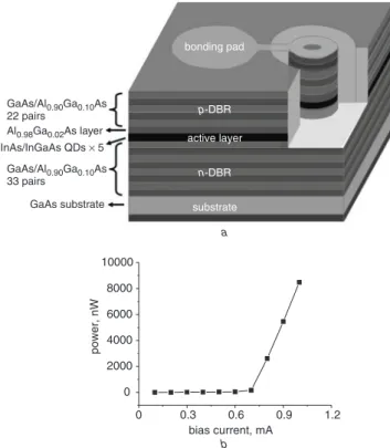
0 0.3 0.6 0.9 1.2 0 2000 4000 6000 8000 10000 power, nW bias current, mA b GaAs/Al0.90Ga0.10As 22 pairs GaAs/Al0.90Ga0.10As 33 pairs GaAs substrate InAs/InGaAs QDs × 5 Al0.98Ga0.02As layer bonding pad p-DBR active layer n-DBR substrate a
Fig. 1 Schematic diagram of QD VCSEL and light-current characteristics a Schematic diagram
b Light-current characteristics
Experiment and results: Fig. 1ashows the schematic diagram of the monolithically singlemode QD VCSEL. The structure is grown on a
GaAs (100) substrate using MBE by NL Nanosemiconductor GmbH (Germany). The fabrication method has been described in our previous works [2, 5]. In addition, the QD VCSEL is hermetically sealed by a standard TO-Can package with a built-in lens. The TO-Can packaged QD VCSEL and the singlemode fibre are assembled by laser welding technique.Fig. 1bshows the light-current characteristics of the QD VCSEL. The threshold current is about 0.7 mA.Fig. 2shows the experimental setup for measuring the optical group delays in the QD VCSEL. A probe signal is generated by a tunable laser modulated with an electro-optical modulator. The signal power is controlled by a variable optical attenuator at the output of the electro-optical modulator. The polarisation of the probe signal is adjusted to reach the maximum time delay in the QD VCSEL. An optical circulator is used to couple the probe signal into the QD VCSEL.
oscilloscope trigger power splitter RF signal generator C PD QD VCSEL DC bias PC tunable laser VA 1 2 3 RFA Mod DC bias OSA OC tunable delay line
Fig. 2 Experimental setup for measuring optical group delays in QD VCSEL
Mod: electro-optic modulator; VA: variable optical attenuator; C: optical circu-lator; OC: optical coupler; PC: polarisation controller; RFA: RF amplifier; PD: photodetector; OSA: optical spectrum analyser
intensity, a.u. time, 20ps/div. ref. 0.6mA 1 0.7 0.9 T=42ps
Fig. 3 Measurements of time delay for 10 GHz probe signal at various bias currents of QD VCSEL
a b –12 dBm –10 intensity, a.u. 1mA T = 36 ps T = 27ps 0.6mA –12 dBm –10 intensity, a.u. time, 20 ps/div. T = 9ps T = 7ps time, 20 ps/div. –15 –14 –13 –12 –11 –10 –9 –8 –7 –10 0 10 20 30 40 50 60 70 delay, ps 1.0mA 0.9mA 0.7mA 0.6mA signal power, dBm
Fig. 4 Waveform at different powers of probe signals; time delays against bias currents of QD VCSEL and optical power of probe signal
a Waveform at different powers of probe signals
b Time delays against bias currents of QD VCSEL and optical power of probe signal
Fig. 3shows the measurements of time delay for a 10 GHz probe signal at the various bias currents of the QD VCSEL. The probe signal is tuned to the resonance of the QD VCSEL cavity, and the signal power
is 14 dBm. Increasing the bias current of the QD VCSEL can increase the time delay of the probe signal. The maximum group delay of 42 ps is observed, and the driving current is at 1 mA.Fig. 4a shows the waveform at different powers of probe signals when the bias current of the QD VCSEL are at 1 and 0.6 mA. The time delays are 36 and 27 ps for 12 and 10 dBm, respectively, when the bias current is at 1 mA. In addition, the time delays against bias currents of the QD VCSEL and the optical power of probe signal are shown inFig. 4b. We observe that the time delay increases as the signal power decreases.
Conclusion: We have experimentally demonstrated tunable optical group delay in a 1.3 mm QD VCSEL at room temperature for the first time. The monolithic QD VCSEL based on GaAs substrate is the fully doped structure. Tunable delays of 42 ps for 10 GHz are achieved by varying the bias current.
Acknowledgments: The authors thank S.-L. Chuang (Department of Electrical and Computer Engineering, University of Illinois at Urbana-Champaign) for useful discussions and A.R. Kovsh (NL Nanosemiconductor GmbH) for his assistance and cooperation in epitaxial growth. This work is supported by the National Science Council, Republic of China, under contract NSC 94-2752-E-009-007-PAE.
#The Institution of Engineering and Technology 2006
26 April 2006
Electronics Letters online no: 20061316 doi: 10.1049/el:20061316
P.C. Peng, C.T. Lin, H.C. Kuo, W.K. Tsai, S. Chi, and S.C. Wang (Department of Photonics and Institute of Electro-Optical Engineer-ing, National Chiao Tung University, 1001 Ta Hsueh Road, Hsinchu, Taiwan 300, Republic of China)
E-mail: [email protected]; [email protected] G. Lin, H.P. Yang, K.F. Lin and J.Y. Chi (Opto-Electronics and System Laboratory, Industrial Technology Research Institute, Hsinchu, Taiwan 300, Republic of China)
References
1 Yang, H.P., Chang, Y.H., Lai, F.I., Yu, H.C., Hsu, Y.J., Lin, G., Hsiao, R.S., Kuo, H.C., Wang, S.C., and Chi, J.Y.: ‘Singlemode InAs quantum dot photonic crystal VCSELs’, Electron. Lett., 2005, 41, (20), pp. 1130–1132
2 Chang, Y.H., Lin, G., Kuo, H.C., Chi, J.Y., and Wang, S.C.: ‘Singlemode monolithically quantum-dot vertical-cavity surface-emitting laser in 1.3 mm with side-mode suppression ratio > 30 dB’. IEEE Lasers and Electro-Optics Society 2005 Annual Mtg (LEOS 2005), Paper No. TuAA4, pp. 400–401, 2005
3 Minin, S., Fisher, M.R., and Chuang, S.L.: ‘Current-controlled group delay using a semiconductor Fabry-Perot amplifier’, Appl. Phys. Lett., 2004, 84, pp. 3238–3240
4 Zhao, X., Palinginis, P., Pesala, B., Chang-Hasnain, C.J., and Hemmer, P.: ‘Tunable ultraslow light in vertical-cavity surface-emitting laser amplifier’, Opt. Express, 2005, 13, pp. 7899–7904
5 Yu, H.C., Chang, S.J., Su, Y.K., Sung, C.P., Lin, Y.W., Yang, H.P., Huang, C.Y., and Wang, J.M.: ‘A simple method for fabrication of high speed vertical cavity surface emitting lasers’, Mater. Sci. Eng. B, 2004, 106, pp. 101–104