國立交通大學
電子工程學系 電子研究所碩士班
碩 士 論 文
以脈波閂鎖器之存活記憶體單元為基礎之低功率維特
比解碼器
A Low-power Viterbi Decoder Based on
Pulse Latch Survivor Memory
學生:李欣儒
指導教授:李鎮宜教授
以脈波閂鎖器之存活記憶體單元為基礎之低功率維特
比解碼器
A Low-power Viterbi Decoder Based on
Pulse Latch Survivor Memory
研 究 生:李欣儒
Student:Xin-Ru Lee
指導教授:李鎮宜教授
Advisor:Chen-Yi Lee
國 立 交 通 大 學
電子工程學系 電子研究所 碩士班
碩 士 論 文
A ThesisSubmitted to Department of Electronics Engineering & Institute Electronics College of Electrical and Computer Engineering
National Chiao Tung University In Partial Fulfillment of the Requirements
for the Degree of Master of Science
in
Electronics Engineering September 2009
以脈波閂鎖器之存活記憶體單元為基礎之低功率維特
比解碼器
學生:李欣儒
指導教授:李鎮宜 教授
國立交通大學
電子工程學系 電子研究所碩士班
摘 要
近來由於無線及可攜式裝置的普及,高速低功率的維特比解碼器成為設計上 重要的考量。為了有效降低維特比解碼器的功率消耗,本論文提出一個脈波閂鎖 器來實現解碼器的記憶體部分。由於電壓低擺伏的優點及通行電晶體的特性,可 降低單一記憶體單元的功率消耗,進而降低資料存取時的功率消耗。模擬結果顯 示,在雜訊比為 3 分貝的環境下,本研究所提出的方法可省下 21%的解碼器功 率消耗與 29%的存活記憶體單元功率消耗。A Low-power Viterbi Decoder Based on
Pulse Latch Survivor Memory
Student:Xin-Ru
Lee Advisor:Dr. Chen-Yi Lee
Department of Electronics Engineering
Institute of Electronics
National Chiao Tung University
ABSTRACT
Recently, a high-speed and low-power Viterbi decoder is needed due to wireless and portable devices. In order to reduce the power consumption of Viterbi decoder, we proposed a full-custom pulse latch as the data storage unit in the survivor memory. Because of the low-swing and the characteristic of pass transistor, the power consumption of single register is reduced, so the power of data access in survivor memory also be reduced. According to the implementation result, 29% of survivor memory power and 21% of overall decoder power could be reduced as Eb/No is 3dB.
誌
謝
時光匆匆,兩年的碩士班生涯即將劃下句點。在實驗室的這兩年裡,讓我學 習到很多研究上的、待人處事的態度與方法。首先要感謝我的指導教授李鎮宜老 師,建立了良好的研究氣氛與實驗室環境,以及耐心的、祥和的指引我的研究方 向,讓我能順利的完成碩士學業。其次要感謝錫嘉老師,給予我自由的研究方向 及努力的目標,在研究上也給予我極大的精神鼓勵,讓我不至於遇到挫折而徬徨 無助。 感謝阿龍學長與義澤學長,在我研究的過程中能給予正確的研究態度,並適 時的給予問題的解答,讓我能順利的完成研究過程。感謝 Si2Lab 及 OCEAN 團隊 的每一份子,在 meeting 時提供了許多的建議,讓我能有信心去解決問題。感謝 團隊裡的所有學長姐、同學、以及學弟妹,有你們的陪伴,讓我在這兩年裡的研 究並不孤單。 最後,感謝我的家人及女友的關心與支持,讓我順利的完成這兩年的碩士生 涯,謝謝你們。
Contents
1 Introduction 1
1.1 Research Motivation . . . 1
1.2 Thesis Organization . . . 2
2 Introduction of Convolutional Code 3 2.1 Convolutional code . . . 3
2.2 Encoding of Convolutional Code . . . 3
2.3 Decoding of Convolutional Code . . . 6
2.3.1 Trellis Diagram of Convolutional Code . . . 6
2.3.2 Viterbi Decoding Algorithm . . . 7
3 Architecture of Viterbi Decoder 9 3.1 Branch Metric Unit . . . 10
3.2 Add-Compare-Select Unit . . . 11
3.2.1 Radix-2 ACS Architecture . . . 11
3.2.2 Radix-2n ACS Architecture . . . 12
3.2.3 CSA Stucture . . . 13
3.3.1 Register-exchange Approach . . . 14
3.3.2 Trace-back Approach . . . 17
4 The Proposed Low-power Viterbi Decoder 23 4.1 Low Power Schemes for Viterbi Decoder . . . 24
4.2 The Design of Low Power Survivor Memory . . . 26
4.2.1 The Differential Cascade Voltage Switch Pulse Latch . . . 27
4.2.2 Implementation Result of DCVS-based Viterbi Decoder . . . 30
4.2.3 The Differential Cascade Voltage Switch Pass-Gate Pulse Latch . . 31
5 Implementation Result 37 5.1 Chip Specification . . . 37
5.2 Comparison with UMC Standard Cell . . . 38
5.3 Comparison with Other Relative Work . . . 39
List of Figures
1.1 Block diagram of a digital communication system . . . 1
2.1 The (2, 1, 2) convolutional code . . . 4
2.2 State diagram of convolutional code in figure 2.1 . . . 6
2.3 Trellis diagram of convolutional code in figure 2.1 . . . 7
3.1 Block diagram of Viterbi decoder . . . 9
3.2 3-bit quantization result . . . 10
3.3 The architecture of branch metric unit . . . 11
3.4 The architecture of radix-2 ACS unit . . . 12
3.5 The 4-state radix-2 and radix-4 trellis diagrams . . . 13
3.6 The architecture of CSA structure . . . 14
3.7 Register-exchange of SMU . . . 15
3.8 The best state approach . . . 15
3.9 The fixed state approach . . . 16
3.10 The majority vote approach . . . 16
3.11 The k-pointer even algorithm structure . . . 19
3.12 The k-pointer odd algorithm structure . . . 20
3.14 The hybrid algorithm structure . . . 22
4.1 The model of SST Viterbi decoding . . . 24
4.2 The survivor path over a noiseless channel . . . 25
4.3 Path merge phenomenon . . . 26
4.4 Path merge of register-exchange approach . . . 27
4.5 Path merge of trece-back approach . . . 28
4.6 The power profiling of conventional decoder at SNR=3.0 . . . 29
4.7 The architecture of master-slave flip-flop . . . 29
4.8 The design of DCVS pulse latch . . . 30
4.9 The design flow of survivor memory . . . 30
4.10 The design of DCVSPG pulse latch . . . 33
4.11 The design of proposed pulse latch . . . 33
4.12 The design of clock gating pulse latch . . . 34
4.13 The design of pulse sharing pulse latch . . . 35
4.14 Power profiling of survivor memory based on pulse sharing pulse latch . . . 36
5.1 The power profiling of proposed decoder . . . 40
List of Tables
3.1 Comparison of different radix ACS unit . . . 13
3.2 Comparison of survivor memory approach . . . 22
4.1 Comparison of Viterbi decoders . . . 31
4.2 Simulation result and comparison of proposed pulse latch . . . 34
4.3 Simulation result of pulse sharing of double pulse latches . . . 35
4.4 Comparison of survivor memories . . . 36
5.1 The Implementation result . . . 38
5.2 Comparison of Viterbi decoders . . . 39
Chapter 1
Introduction
1.1
Research Motivation
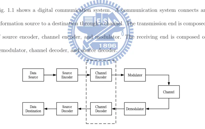
Fig. 1.1 shows a digital communication system. A communication system connects an information source to a destination through a channel. The transmission end is composed of source encoder, channel encoder, and modulator. The receiving end is composed of demodulator, channel decoder, and source decoder.
Figure 1.1: Block diagram of a digital communication system
as it passes through the channel. In order to eliminate those effects, the channel encoder transforms the source codeword into channel codeword by adding some redundant bits. These redundant bits could be used for error detection and error correcting. Next, the modulator converts the channel codeword into analog signals and transmits through the channel. In the receiver end, the demodulator, making some errors because of channel noise, generates the receive sequence. The channel decoder uses those redundant bits to correct the errors in the receive sequence, maintaining the performance of overall system. Viterbi decoder is widely used in channel coding. Modern wireless communication systems are required to transmit in high data rate and low power. But high data rate and power consumption are still challenges. So how to reduce power and achieve high throughput are our design goals. In this thesis, some methods are proposed for a low-power Viterbi decoder.
1.2
Thesis Organization
This thesis consists of five chapters. In chapter 2, the fundamental convolutional code and Viterbi algorithms [1] are introduced, the architectures of general Viterbi decoder are described in chapter 3. The differential trellis decoding algorithm is introduced in chapter4. In chapter 5 the proposed low-power Viterbi decoder will be presented, including performance results, and hardware architectures. Finally, the conclusion and future work are given in chapter 6.
Chapter 2
Introduction of Convolutional Code
2.1
Convolutional code
Convolutional codes are widely used in error control coding for digital communication sys-tem, because they have powerful error correcting capabilities and low hardware complexi-ties. The Viterbi algorithm, an optimal decoding method, uses maximum-likelyhood(ML) decoding and becomes the popular method to deal with convolutional codes. All of above will be introduced in this chapter.
2.2
Encoding of Convolutional Code
A convolutional encoder contains memory. Its output data depends not only on the input at that time but the previous inputs. A general convolutional encoder can be specified as (n, k, m) format, which n stands for the number of outputs, k stands for the number of inputs, and m is the number of memories, the coding rate is k/n respectively. Fig. 2.1 shows (2, 1, 2) convolutional encoder, it produces two output coded bits for
one information bit. In this example, the inputs of encoder is u = (u1, u2, u3,· · · ), the 3, 2, 1
u u
u
… 1 1 1 1, 2, 3,C
C
C
… 2 2 2 1, 2, 3,C
C
C
…Figure 2.1: The (2, 1, 2) convolutional code
corresponding output sequence is C = (C1
1, C12, C21, C22, C31, C32,· · · ). For time index i, the
coded bits C1
i and Ci2 are generated by
Ci1 = ui⊕ ui−1⊕ ui−2
C2
i = ui⊕ ui−2
(2.1) In general, the (n, k, m) convolutional code can be seen as the convolution of input sequence with encoder impulse responses. The impulse responses can be formulated as follows: g1 = (g1 0, g11, g12,· · · , g1m) ... gn= (gn 0, gn1, g2,n· · · , gnm) (2.2)
For the matrix form, we can arrange the impulse responses in the form of
G= g01 g11 · · · g1 m g02 g21 · · · gm2 · · · g0n g1n · · · gnm g01 g11 · · · g1 m g20 g12 · · · g2m · · · g0n gn1 · · · gnm · · · · · · · · · · · · (2.3)
so the encoding process can be presented as C = uG, where C are the coded bit sequences, u are the information sequences, and G is the generator matrix.
Another format which describes the impulse responses of (n, k, m)convolutional code is the generator polynomial, and the encoding process can be seen the polynomial multiplication as below:
C1(D) = u(D)g1(D)
C2(D) = u(D)g2(D)
(2.4) where g1(D) and g2(D) are the generator polynomials, the coefficient of each term is
dependent on whether a connection between register and modulu-2 adder, and D means the unit delay. There is a simple example for Fig. 2.1, the input sequence can be repre-sented as
u(D) = 1 + D2+ D3+ D4 (2.5) and the generator polynomials are
g1(D) = 1 + D + D2
g2(D) = 1 + D2
(2.6)
the encoding process becomes
C1(D) = (1 + D2+ D3+ D4)(1 + D + D2) = 1 + D + D4+ D6
C2(D) = (1 + D2+ D3+ D4)(1 + D2) = 1 + D3+ D5+ D6
(2.7)
so the codeword sequences are
2.3
Decoding of Convolutional Code
In 1967, Viterbi proposed a decoding algorithm for convolutional code that has become a well-known as Viterbi algorithm.Then, Forney [2] proved the Viterbi algorithm was in fact that a maximum likelyhood(ML) decoding algorithm. In this section, the Viterbi algorithm and decoding method will be introduced.
2.3.1
Trellis Diagram of Convolutional Code
In the convolutional code, the encoder has finite memory that stores information of the past, and we define at any time instant, the information symbol stored in the encoder as a state. Because the information are shifted into memory serially, there is a transition from one state to another, so the encoder can be seen as a finite-state machine. Fig. 2.2 shows the state diagram of convolutional code in Fig. 2.1.
01
00
11
10
1/11 0/00 1/00 1/11 0/10 1/01 1/10 0/01Figure 2.2: State diagram of convolutional code in figure 2.1
00 01 10 11 00 01 10 11 00 00 10 00 01 10 11 00 01 10 11 00 01 10 11
0
u
=
1 u =Time=0 Time=1 Time=2 Time=3 Time=4 Time=5 Time=6
00 01 10 11 00 00 00 00 00 00 00 00 00 11 11 11 11 11 11 11 11 11 01 01 01 01 01 01 01 01 10 10 10 10 10 10 10 10 10
Figure 2.3: Trellis diagram of convolutional code in figure 2.1
the codeword sequences. Therefore, another representation of convolutional code called trellis diagram,which is obtained by considering the dimension of time. With the trellis diagram, it is easy to illustrate decoding process. Fig. 2.3 shows the trellis diagram of convolutional code in figure 2.1.
2.3.2
Viterbi Decoding Algorithm
The goal of Viterbi algorithm is to maximize the probability of P (r|c), where r stands for received sequences from channel, c stands for codewords from encoder. According to the maximum likelyhood decoding, Viterbi proposed an algorithm to compute the minimum Euclidean distance as time goes on. There are two basic measures defined in the Viterbi algorithm, which are branch metric BMt
x→y and path matric P Myt. At time t, this two
measures are computed as follows:
BMx→yt = n X i=1 (rti − c t i)2 (2.9)
P Myt = min(P Mt−1 x→y+ BM t x→y, P Mz→yt−1 + BM t z→y,· · · ) (2.10) BMt
x→y denotes the Euclidean distance between state x and state y at time t, and P Myt
denotes the minimum distance along the decoding process. In other words, the path met-ric is the accumulation of branch metmet-rics that across the corresponding paths. Therefore, the Viterbi algorithm can find the minimum path metric at each time instant.
For a (n, k, m) convolutional code, the Viterbi decoding algorithm process is described as follows:
1. Initially, set path metrics as
P M00 = 0, P M10 = ∞, P M20 = ∞, · · · , P M20m
−1 = ∞
2. At any time instant, update the path metrics P Myt = min(P Mt−1 x→y + BM t x→y, P Mz→yt−1 + BM t z→y,· · · )|y ∈ (0, 1, · · · , 2 m− 1)
and store the survivor. The survivor means the decision bit corresponding to the chosen branch from all branches merge into state y.
Chapter 3
Architecture of Viterbi Decoder
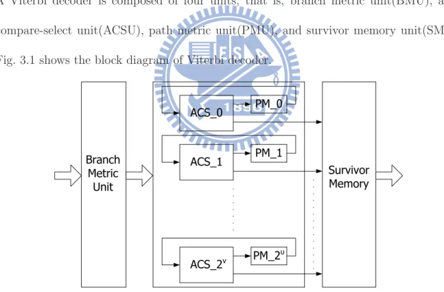
In this chapter, the basic hardware implementation of Viterbi decoder will be introduced. A Viterbi decoder is composed of four units, that is, branch metric unit(BMU), add-compare-select unit(ACSU), path metric unit(PMU), and survivor memory unit(SMU). Fig. 3.1 shows the block diagram of Viterbi decoder.
ACS_0 Branch Metric Unit Survivor Memory PM_0 ACS_1 PM_1 ACS_2ν PM_2 υ
3.1
Branch Metric Unit
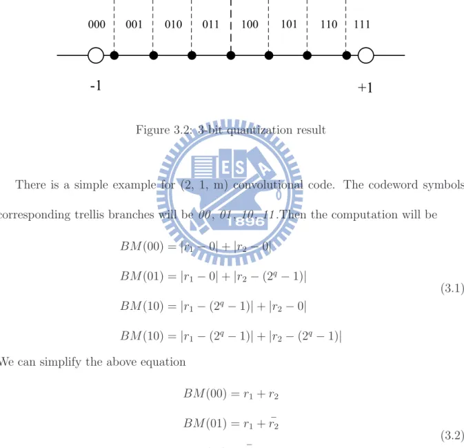
This unit generates all branch metrics from received symbol. Usually, we adopt q-bit quantization when receiving the transmitted symbol, to indicate received values from channel. The larger q is, the better the performance of decoder, but the complexity also increases. In general, considering the tradeoff between performance and cost, we usually use 3-bit quantization soft decision. Fig. 3.2 shows the quantization result.
000
+1
-1
001 010 011 100 101 110 111
Figure 3.2: 3-bit quantization result
There is a simple example for (2, 1, m) convolutional code. The codeword symbols corresponding trellis branches will be 00 , 01 , 10 , 11 .Then the computation will be
BM(00) = |r1− 0| + |r2− 0|
BM(01) = |r1− 0| + |r2− (2q− 1)|
BM(10) = |r1− (2q− 1)| + |r2− 0|
BM(10) = |r1− (2q− 1)| + |r2− (2q− 1)|
(3.1)
We can simplify the above equation
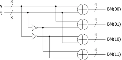
BM(00) = r1+ r2 BM(01) = r1+ − r2 BM(10) =r1 +r− 2 BM(11) =r−1 +r−2 (3.2)
1 2 BM(00) BM(01) BM(10) BM(11) 4 4 4 4 3 3
Figure 3.3: The architecture of branch metric unit
3.2
Add-Compare-Select Unit
There are many issues in designing an ACS unit because the ACS unit is the key compo-nent in Viterbi decoder to calculate the minimum path metric and estimate the survivor path. As modern communication systems require a high data rate condition, the fully parallel architecture is prefer. In the following, we introduce the most popular architec-tures.
3.2.1
Radix-2 ACS Architecture
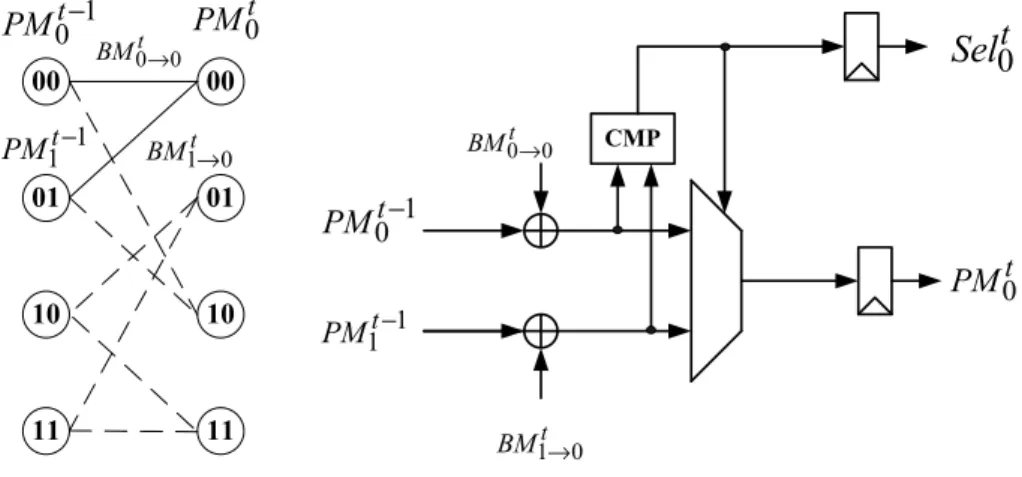
Radix-2 ACS architecture is the simplest structure of Viterbi ACS unit. From Fig. 2.3, we see that for every state in any time instant, there are two incoming paths. In ACS unit, it adds the previous path metric with branch metric for every path, then, it compares all the paths to choose the minimum partial path metric. And all compared results of ACS units are saved in the survivor memory. Moreover, the minimum path metric is selected as the new path metric. Fig. 3.4 shows the trellis diagram and ACS structure for state 0 of 4-state concolutional code. In Fig. 3.4, we find the state 0 has two predecessor states
state 0 and state 1. First, the previous path metric and branch metric are added. Then, the two results are compared to decide which one is the survivor and which path metric is updated. Finally, the updated path metric becomes the predecessor path at next time.
CMP 0 t PM 1 1 t PM − 1 0 t PM − 0 0 t BM → 1 0 t BM→ 0 t
Sel
00 01 10 11 00 01 10 11 1 0 t PM − 1 1 t PM − 0 0 t BM → 1 0 t BM→ 0 t PMFigure 3.4: The architecture of radix-2 ACS unit
3.2.2
Radix-
2
nACS Architecture
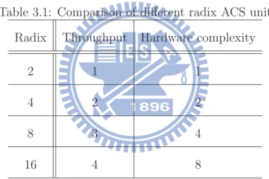
ACS unit is the bottleneck for a high-speed Viterbi decoder due to the recursive operation. For high-speed design, decreasing the critical path of ACS unit is a solution. So the high radix architectures [3] [4] are popular. The high radix structure unrolls the ACS loop in order to perform multi-step of trellis in one clock cycle. Fig. 3.5 shows the 4-state radix-2 and radix-4 architectures. We see that in radix-4 architectures, it combines two stages of radix-2 trellis into one stage radix-4 trellis, so the radix-4 structure is two times faster than radix-2 structure. In the same way, we can obtain a higher radix structure. For one clock cycle, a radix-2n structure can achieve n times speed up than a radix-2 structure.
However, the number of branches for every state, the complexity of comparator and multiplexer, are increasing. So the overall complexity of ACS unit also increases n times.
t-2
t-1
t
t-2
t
Figure 3.5: The 4-state radix-2 and radix-4 trellis diagrams
Table 3.1 shows the comparison of different radix ACS unit.
Table 3.1: Comparison of different radix ACS unit Radix Throughput Hardware complexity
2 1 1
4 2 2
8 3 4
16 4 8
3.2.3
CSA Stucture
In this subsection, another ACS structure, called compare-select-add (CSA) structure [5], is introduced. In CSA structure, the addition is postponed to the last procedure. In this way, the recursive operation can be broken, and the critical path is decreased. Fig. 3.6 shows the CSA architecture.
( ) 0 n s D ( ) 32 n s D ( ) 0 n s PM ( ) 32 n s PM ( 1) 0 n s PM − ( 1) 1 n s PM − BM ∆ BM ∆ 00 BM 11 BM
Figure 3.6: The architecture of CSA structure
3.3
Survivor Memory Unit
In Survivor memory unit, there are two well-known approaches, one is register-exchange(RE) method, and the other is trace-back(TB) [6] method. This section will introduce these methods.
3.3.1
Register-exchange Approach
The register-exchange approach is the simplest used technique which assigns a set of regis-ters to each state. Fig. 3.7 shows an example. These regisregis-ters record the decoded outputs which are produced by survivor paths. At each time step, these registers will change their contents to update new decoded outputs. Therefore, this approach doesn’t need to trace back the survivor path, that is, the latency will reduce dramatically. However, due to exchaging every register, the power consumption is large, it is not power efficient.
In register-exchange approach, there are three methods for implementation. First is best state approach, second is fixed state approach, and last is majority vote approach. In
00 10 110 000 010 100 1 0000 0110 1000 1110 0 0000 0111 1011 1111 0011 0111 1000 1101 Decoded bit t=0 t=1 t=2 t=3 t=4 t=5 0 1
Figure 3.7: Register-exchange of SMU
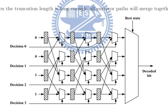
conventional method, best state approach is be used according to maximum likelyhood algorithm. Fig. 3.8 shows the architecture of best state approach with truncation length 4. When the truncation length is long enough, all survivor paths will merge together. In
0 0 1 1 Decision 0 Decision 1 Decision 2 Decision 3 Best state Decoded bit
Figure 3.8: The best state approach
the same time, we don’t need to search the best state. Instead, one can choose the con-tent of state 0 as decoded bit. However, more registers are required to save long enough
survivor path. Fig. 3.9 shows the architecture of fixed state approach with truncation length 4. A compromising approach between best state approach and fixed state appoach
0 0 1 1 Decision 0 Decision 1 Decision 2 Decision 3 Decoded bit
Figure 3.9: The fixed state approach
is majority vote approach. In this method, the best state search is replaced by majority vote circuit. That is, at truncation length L, if the number of 1’s of the registers is larger than the number of 0’s of the registers, the decoded bit is 1, vice versa. Fig. 3.10 shows the architecture of majority vote approach with truncation length 4.
0 0 1 1 Decision 0 Decision 1 Decision 2 Decision 3 Decoded bit M a jo ri ty v o te c ir cu it
3.3.2
Trace-back Approach
Unlike register-exchange approach, the trace-back approach only stores the comparison results corresponding to one stage in a trellis diagram, and after the truncation length reaching, the decoded bits are produced by tracebacking the trellis diagram. In this method, the latency will increase, but it consumes less power and suits for portable devices. There are three types of operations performed inside the trace-back unit.
1. Writing(WR):The decisions made by the ACS are written into lacations correspod-ing to the states. The write pointer advances forward as ACS operations move from one stage to the next in the trellis, and data are written to locations just freed by the decode read operation.
2. Traceback Read(TB): Pointer values from this operation are not output as decoded values, instead they are used to ensure that all paths have converged with some high probability, so that actual decoding amy take place. The traceback operation is usually run to a predetermined depth T before being used to initiate the decode read operation.
3. Decode Read(DC):When The TB operation finishing, the decode read operation begin to decode bits in reverse order. This operation proceeds in exactly the same fashion as TB operation, but on older data. The values from this operation are stored in a last-in-first-out(LIFO) memory, and sent out when DC operation finish-ing.
There are four types of well-known trace-back algorithm , that is, the k-pointer even algo-rithm, the k-pointer odd algoalgo-rithm, the one-pointer algoalgo-rithm, and the hybrid algorithm. In the following, we introduce these four methods.
1. The k-Pointer Even Algorithm:
Fig. 3.11 shows the structure of k-pointer even algorithm with k=3. The memory is divided into 2k memory banks, each of size L
k−1. Each read pointer is used to
perform the TB operation in two memory banks, and the DC in one memory bank. First, the WR operation is performed in the first three memory banks. Then, the TB operation in the third memory bank is started, at the same time, the WR operation continues in the fourth memory bank. The trace-back operation continues across the third and the second banks, while the ACS decisions are written to the fourth and the fifth banks. Note that the combined length of the second and the third banks is exactly the truncation length L. Hence, a merging state at the first memory bank is determined by trace-back operation of length L. Then, the decoding operation starts and the decoded bits are generated in reverse order. The latency of the k-pointer even approach is k−12kL, which is the time delay from writing the first column to decoding the first symbol. In this example of 3-pointer even algorithm, the latency is 3L as shown in Fig. 3.11. With this decoding process, one can generate the decoded bits sequentially.
2. The k-Pointer Odd Algorithm:
Fig. 3.12 shows the structure of k-pointer odd approach with k=3. There are 2k-1 memory banks, each of size L
k−1. The decoding process of the k-pointer odd approach
is similar to the k-pointer even approach. The main difference is that the k-pointer odd approach combines decoding operation and write operation into one memory bank.
1 L/2 1 L/2 1 L/2 1 L/2 1 L/2 1 L/2 L/2 L Time 3L/2 2L 5L/2 3L 4L 9L/2 7L/2 : WR : TB : DC
Bank 0 Bank 1 Bank 2 Bank 3 Bank 4 Bank 5
0
2n-1 : Idle
0 0 0
2n-1 2n-1 2n-1
Figure 3.11: The k-pointer even algorithm structure
The one-pointer approach differs significantly from the k-pointer approach. Instead of the k-pointer, this approach adopts only one read pointer but accelerating the read operation. For example, if a k-pointer approach is converted to one-pointer approach, the trace-back and decoding operations need to be performed k times faster. However, the number of memory banks can be reduced. Fig. 3.13 shows the memory structure and operation of one-pointer approach with k=3. First, write operation is executed. After write operation is completed in the third memory bank, the read pointer starts trace-back operation in the third memory bank at the best path metric. At the same time, write operation continues in the fourth memory bank. Notice that the read operation is 3 times faster than the write operation.
1 L/2 1 L/2 1 L/2 1 L/2 1 L/2 L/2 L Time 3L/2 2L 5L/2 3L 4L 9L/2 7L/2 5L 11L/2
Bank 0 Bank 1 Bank 2 Bank 3 Bank 4
: WR : TB : DC
0
2n-1 : Idle
0 0 0
2n-1 2n-1 2n-1
Figure 3.12: The k-pointer odd algorithm structure
Therefore, when the write operation finishes in the fourth memory bank, the trace-back and decoding operation must be completed in the other three memory banks. By a similar fashion, the decoded bits can be generated sequentially. Furthermore, the number of memory banks and latency of this example are 4 and 2L respectively, which are smaller than those of the 3-pointer approach. In conclusion, if a k-pointer approach is converted to one-pointer approach, k+1 memory banks are needed, each of size L
k−1, and the latency is k+1 k−1L
1 L/2 1 L/2 1 L/2 1 L/2 L/2 L Time 3L/2 2L 5L/2 3L 4L 7L/2
Bank 0 Bank 1 Bank 2 Bank 3
: WR : TB : DC
0
2n-1 : Idle
0 0 0
2n-1 2n-1 2n-1
Figure 3.13: The one-pointer algorithm structure
The hybrid trace-back approach combines the k-pointer approach and one-pointer approach. That is, the trace-back and decoding operations become k1 times faster to determine the merging state and decoded bits, which is like the one-pointer approach. In addition, it uses k2 read pointers simultaneously when trace-back and decoding operations are executed, which is like the k-pointer approach. Fig. 3.14 shows the memory structure and operation of even hybrid approach with k1=2 and k2=2. In this approach, the number of memory banks are k2(k1+1) and k2(k1+1)-1 for the even hybrid approach and the odd hybrid approach, respectively. Each memory bank size is L
k1k2−1 and the latency is
k2(k1+1)L k1k2−1 .
Table 3.2: Comparison of survivor memory approach
register-exchange k-pointer even k-pointer odd one-pointer hybrid Memory size L∗ 2n 2k k−1L∗ 2 n k+1 k−1L∗ 2 n 2k−1 k−1L∗ 2 n k2(k1+1)L k1k2−1 ∗ 2 n Latency T 2k k−1L k+1 k−1L 2k k−1L k2(k1+1)L k1k2−1 1 L/3 1 L/3 1 L/3 1 L/3 1 L/3 1 L/3 L/6 2L/6 Time 3L/6 4L/6 5L/6 L 8L/6 9L/6 7L/6 10L/6 11L/6 2L 13L/6 : WR : TB : DC 0 2n-1 : Idle 0 0 0 2n-1 2n-1 2n-1
Bank 0 Bank 1 Bank 2 Bank 3 Bank 4 Bank 5
Chapter 4
The Proposed Low-power Viterbi
Decoder
In this chapter, some proposed designs are presented. In the Viterbi decoder, the survivor memory unit is the power critical part because of data accessing. In order to reduce the power consumption of survivor memory, a low-power pulse latch is proposed for our decoder design. Based on the proposed design, the power saving of the survivor memory unit is increasing.
At the beginning of the chapter, we will describe state-of-the-arts for low-power Viterbi decoder. Then, the proposed low-power pulse latch will be introduced. Next, some simulation and implementation results are shown. Finally, the comparison between some different design will be shown.
4.1
Low Power Schemes for Viterbi Decoder
In this section, we will introduce some low power schemes for the Viterbi decoder. First is the scarce-state-transition (SST) algorithm [7]. SST technique could reduce the state transition activities as channel is high SNR condition. Fig. 4.1 shows the architecture of SST Viterbi decoder and some extra circuits are needed: The pre-decoder and re-encoder. The pre-decoder provides the inverse function of convolutional encoder to pre-decodes the channel values, and the re-encoder is the same as convolutional encoder.
Viterbi decoder Re-encoder Pre-decoder Decoded bits Channel values
Figure 4.1: The model of SST Viterbi decoding
The SST decoding is described as follows: First, the channel values are pre-decoded by the pre-decoder. Then, the pre-decoded bits is send to the re-encoder to re-encode. The new decoder inputs are composed of the re-encoded bits and the channel values. Finally, the decoded bits are the modulo-2 addition of pre-decoded bits and thr output of Viterbi decoder.
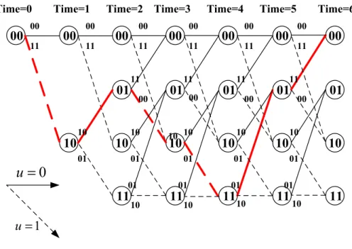
The SST algorithm performs a transformation of channel values. The input sequences of Viterbi decoder are almost zero sequences as channel condition is good enough. As a result, the state transition activities is reduced and the survivor path is nearly passed through zero state as Fig. 4.2. Therefore, the dynamic power is reduced.
Another low-power technique is the path merge algorithm. In practical, the length of information is very large. To reduce the storage requirement, the survivor path should
Conventional Decoder
SST Decoder
Figure 4.2: The survivor path over a noiseless channel
be truncated to finite length. As truncation length is long enough, all survivor paths will merge together, as Fig. 4.3 shows. so some low-power techniques are proposed.
Based on register-exchange method, Lin et.al. [7] proposed a path detection unit to detect path merge phenomenon. When the survivor paths are merged together, the clock gating technique is applied to survivor memory to reduce the power consumption. Fig 4.4 shows the decoding technique.
Based on trace-back method, Lin et.al. [5] proposed a low-power technique by using the buffer to store decisions of previous trace-back result. Next time, the trace-back results will update the contents of buffer when decisions are different. On the contrary, when the trace-back results is the same with the contents of buffer, the access of survivor memory is stopped. Fig. 4.5 shows the decoding technique. According to above methods,
L Merged
Point N
Figure 4.3: Path merge phenomenon
the power of survivor memory could be reduced.
4.2
The Design of Low Power Survivor Memory
Although [5] [7] could achieve low-power scheme, the power of register is still not op-timized. In long constrain length condition, the state numbers and truncation length are increased, so the number of registers also increases. In another word, the puntured convolutional codes are necessary for different coding rate of some standards. In order to maintain the system performance, the truncation length will be increased, so the number of registers also increase. In this way, register optimization is still necessary. Due to the data storage, registers are widely used in the design of Viterbi decoder. In Fig. 3.9, the survivor memory of decoder based on register-exchange method is composed of registers. Because of registers turning on and turning off, the survivor memory is the most power critical part of decoder. In Fig. 4.6, we show the power analysis of conventional Viteri decoder.
Clock Gating G2 G3 G4 G0 G1 1'b0 S0 S1 S2 S3 OUT D0~3 D4~7 D8~11 D60~63 Merge Stage Path Merging Detection Unit
Figure 4.4: Path merge of register-exchange approach
4.2.1
The Differential Cascade Voltage Switch Pulse Latch
In order to design a low-power decoder, the design of register is a problem, so a full-custom register is an appropriate design. There are three major types of registers: master-slave flip-flop, pulse register [8], sense-amplifier-based register [9]. Fig. 4.7 shows the master-slave flip-flop, it is composed of a negative latch (master) with a positive latch (master-slave) to cascade together. The sense-amplifier-based register is often used in memory cores and in low-swing bus driver, but the more complex circuit and the more transistors are its drawbacks. The smaller clock loadings and fewer transistors are the advantages of pulse register. However, the internal node capacitances cause the power dissipation out of our
survivor memory control compare data out buffer ... state x state y
Figure 4.5: Path merge of trece-back approach
expectation. Recently, a edge-trigger latch (ETL) is popular for its smaller pulse width, and the latch is transparent during pulse active, the behavior of ETL is just like a flip-flop. In our Viterbi decoder design, we first adopt a full-custom pulse latch, called differ-ential cascade voltage switch (DCVS) pulse latch [10]. Fig. 4.8 shows the design of this pulse latch. The footer is added to the bottom of inverter chain to prevent full swing (Vdd to Vt) for saving power. Another, a small pulse is generated by the pulse generator
to trigger the latch, just like Fig. 4.8 shows. Finally, the pulse can be shared to another latch, that is, two latches can be triggered by just one pulse generator.
In the design of Viterbi decoder, we usually adopt standard cell design flow to use standard cells to accomplish the decoder. However, due to using the full-custom pulse latch, the cell characterization for the pulse latch must be finished firstly, so extending our design flow to finish our work is necessary. First, we need to develop a library file and a library exchange format (LEF) file to check the timing and physical attributes for the pulse latch. We adopt spice simulation to help us to check function, also to finish timing
Survivor memory 72% ACS 18% PM Unit 5% BM unit 5% Internal power 55% Switching power 43% Leakage power 2%
power profilig of Survivor memory others
48%
register 52%
Figure 4.6: The power profiling of conventional decoder at SNR=3.0
and power data extraction. After the cell characterization, we can use the pulse latch for the standard cell design flow to implement the decoder design. But in the synthesis stage and P&R stage, we should notice that some constraints to use the pulse latch are necessary. Fig. 4.9 shows our design flow.
CLK CLK CLK CLK CLK CLK CLK CLK D Q
VDD CLK VDD Q D CLK CLKb pulse CLKb
Figure 4.8: The design of DCVS pulse latch
Layout Spice simulation & check function
. lib & . lef extraction RTL implementation Synthesis Placement & route Post-layout simulation Spice pre -sim check Flow start Flow end
Figure 4.9: The design flow of survivor memory
4.2.2
Implementation Result of DCVS-based Viterbi Decoder
This section will show the implementation result of of DCVS-based Viterbi decoder. Ac-cording to the cell characterization results in section 4.3.1, we adopt the (3, 1, 6) con-volutional code for UWB system with 3-bit soft-decision and 13 code rate, we also select 128 as the truncation length in our design. Table 4.1 lists the design parameter of the decoder, also shows the comparison of our work.
Table 4.1: Comparison of Viterbi decoders
Standard cell 1 DCVS-based
Technology UMC 90-nm process UMC 90-nm process
State no. 64 64
Gate count 126.8k 143.38k ACS architecture Radix-4 Radix-4 Operating frequency (MHz) 250 250
Core area (mm2) 0.4225 0.429
Power2(mW) 71.78 87.614
Density 96.11% 94.6%
Buffer no. 14740 3365
1 UMC low-power cell: LDFQM2N
2 Post-layout simulation, SNR=3.0dB, 0.9v, 250MHz
4.2.3
The Differential Cascade Voltage Switch Pass-Gate Pulse
Latch
In table 4.1, the power consumption of DCVS-based decoder is more than conventional decoder, but the number of buffer is smaller. So in order to achieve low power target and preserve smaller buffers, we have to make some effort on low power cell. A differential cascade voltage switch with the pass-gate (DCVSPG) pulse latch is another solution. It uses the pass transistors as inputs so fewer transistors are needed, and two diode transistors prevent full-swing. So the power consumption will be smaller. Fig. 4.10 shows the circuit of design. During the spice simulation, the amazing power reduction is
expressed. Table 4.2 displays the simulation result.
Moreover, we propose a modified circuit to achieve more power reduction. The drains of three NMOS transistors could be connected together, and exchange the connection of clock and clock bar. In this way, the voltage swing could be less than conventional DCVSPG pulse latch, as Fig. 4.11 shows. Finally, we also propose two further improve-ments. One is the gated clock pulse latch in Fig. 4.12, the main idea is we turn off the pulse generator by adding an XNOR gate when the input and output of pulse latch are the same. During the simulation, we found that the power consumption is more than conventional DCVSPG pulse latch because of the glitch problem. So we propose another improvement, the pulse generator shared pulse latch. Based on the generator could be shared, we combine two pulse latches but only one pulse generator in this approach, so some power dissipation could be saved. Fig. 4.13 shows the improved result. According the simulation result in the Table 4.3, the power reduction of single DCVSPG pulse latch can achieve 52%. Based on shared genetrator, we also propose the low-power survivor memory. In spice simulation, the power consumption could be reduced 21%, the design parameters and comparison are appeared in table 4.4. From the power profiling in the Fig. 4.14, the power saving of survivor memory is 45% based on the pulse generator shar-ing. In the future, we will consider proper transistor size of pulse generator to have enough driving ability in the Viterbi decoder and make this pulse generator sharing method can be one of the candidate for low power design.
VDD
D
VDD
Q
CLK
Figure 4.10: The design of DCVSPG pulse latch
VDD
D
VDD
Q
CLK
Table 4.2: Simulation result and comparison of proposed pulse latch Pre-layout power Post-layout power Cell area Standard cell 2 5.1504 µW 6.2084 µW 12.701 mm2
DCVS 4.6662 µW 7.3798 µW 13.406 mm2
DCVSPG 3.5061 µW -
-Proposal 3.3315 µW 4.590 µW 9.3744 mm2 1 TT corner, 1.0v, 25◦C, clock rate: 250MHz, output loading: 8.36f 2 UMC low-power cell: LDFQM2N
VDD D VDD Q CLK VDD D Q
VDD D1 VDD Q1 CLK D2 VDD Q2
Figure 4.13: The design of pulse sharing pulse latch
Table 4.3: Simulation result of pulse sharing of double pulse latches Without sharing With sharing
Standard cell 2 10.3142 µW
-DCVS 9.306 µW 7.3282 µW DCVSPG 7.0423 µW 5.7679 µW Proposal 6.6634 µW 5.5766 µW
1 TT corner, 1.0v, 25◦C, 250MHz, output loading
is 8.36f
Table 4.4: Comparison of survivor memories
Standard cell 1 Without sharing With sharing
Technology UMC 90-nm process UMC 90-nm process UMC 90-nm process
State no. 64 64 64
ACS architecture Radix-4 Radix-4 Radix-4 Operating frequency (MHz) 250 250 250
Power 2(mW) 38.12 30.58 27.76
1 UMC low-power cell: LDFQM2N 2 Pre-simulation @SNR=3.0dB, 0.9v
Standard cell (LDFQM2N)
The power of register :19.83 mW
Proposed pulse latch
The power of register :9.47 mW
others
48%
register
52%
others
66%
register
34%
Chapter 5
Implementation Result
5.1
Chip Specification
Based on the low-power cell in section 4.2.3, we proposed a low-power Viterbi decoder for UWB system. The primary chip specification of decoder is given in Table 5.1, which is implemented by mixed-design flow in UMC 90-nm 1P9M standard CMOS process. The total gate count is 119k and core size is 0.372 mm2, the survivor memory occupied 66%
in our design. Fig. 5.1 shows the power profiling of proposed decoder and Fig. 5.2 is the layout photo. The operating frequency can achieve 250MHz and the throughput is 500Mb/s which meets the requirement of UWB system. By the proposed DCVSPG pulse latch, the power consumption, operated at 250MHz with 0.9V supply voltage, 3dB SNR, is 56.86mW which is estimated by post-layout simulation. Also, the power saving could be achieved 21% which compare with UMC standard cell-based Viterbi decoder.
Table 5.1: The Implementation result
Technology UMC 90-nm 1P9M CMOS process
State no. 64
Gate count 119.2k ACS architecture Radix-4
Soft-decision 3-bit PM width 9-bit Operating frequency (MHz) 250 Core area (mm2) 0.372 Power1(mW) 56.86 Density 92.39% 1 Post-layout simulation, SNR=3.0dB, 0.9v, 250MHz
5.2
Comparison with UMC Standard Cell
This section will show the comparison of DCVSPG-based Viterbi decoder with UMC standard cell. We adopt the (3, 1, 6) convolutional code for UWB system with 3-bit soft-decision and 1
3 code rate, we also select 128 as the truncation length in our design.
Table 5.2 lists the design parameter of the decoder, also shows the comparison of our work. To compare with UMC standard cell-based decoder, our Proposed Viterbi decoder is lower hardware complexity and power efficient.
Table 5.2: Comparison of Viterbi decoders
Standard cell 1 Proposal
Technology UMC 90-nm process UMC 90-nm process
State no. 64 64
Gate count 126.8k 119.21k ACS architecture Radix-4 Radix-4 Operating frequency (MHz) 250 250
Core area (mm2) 0.4225 0.372
Power2(mW) 71.78 56.86
Density 96.11% 92.39%
1 UMC low-power cell: LDFQM2N
2 Post-layout simulation, SNR=3.0dB, 0.9v, 250MHz
5.3
Comparison with Other Relative Work
Some of the published Viterbi decoders are list in Table 5.3. According to the power efficient row, the low power design can be achieved in our implementation. For the ref. [7], the SST algorithm and path merge techniques are used. The former technique could reduce the state transition activity in high SNR condition, and the latter technique could reduce the power of survivor memory because of clock gating. According to this two methods, more power reduction is achieved. So in the future, we will combine the techniques with our work together to achieve ultra low-power scheme.
BM unit
5%
PM Unit
5%
ACS
18%
Survivor
memory
72%
SMU
66%
BMU
6%
PMU
7%
ACSU
21%
Proposed decoder
Conventional decoder
S
Table 5.3: Comparison of Viterbi decoders
Proposal TCAS I′07 [11] VLSI−DAT′09 [12] VLSI−DAT07 [7]
Technology 90-nm process 0.13-µm process 0.18-µm process 90-nm process
State no. 64 64 64 64
Truncation 128 40 36 64
length (TL)
Code rate 13 12 12 13
ACS architecture Radix-4 Radix-2 N/A Radix-4
Operating 250 200 100 250
frequency (MHz)
Gate count 119.207k 49.4k N/A N/A
Core area (mm2) 0.3721 N/A 0.69 0.25
Power (mW) 56.86 1(37.53 2) 49.94 (36.42 2) 58 (12.08 2) 28.52 (4.85 2)
Energy - (0.5862) - (2.6942) - (1.0362) - (0.152 2)
efficiency (pJ/TL/bit)
1 Post-layout simulation @SNR=3.0dB, 250MHz, 0.9v 2 Survivor memory only
Chapter 6
Conclusion and Future Work
In this thesis, a low-power decoder based on the low-power pulse latch survivor memory design is proposed. With this low-power pulse latch, the power consumption of data access in the survivor memory is reduced. Experimental results indicate the power reduction of the whole decoder and the survivor memory can achieve 21% and 29% as Eb/N
0 is 3dB,
which compare to UMC standard cell-based Viterbi decoder. In addition to reducing the power consumption, our proposal also reduces 8% gate count of the whole decoder.
In the future, we want to design a high-speed and low-power Viterbi decoder to apply to IEEE 802.15.3c standard. In the high-speed issue, the radix-4x4 is a feasible solution. And in the low-power method, we will combine the low-power pulse latch with scarce-state-transition algorithm, and path merge methodology to attain more power reduction. Also, we will finish the pulse sharing-based Viterbi decoder.
Bibliography
[1] A. J. Viterbi, “Error bounds for convolutional codes and asymptotically optimal decoding algorithm,” IEEE Trans. Inform. Theory, vol. IT-13, no. 2, pp. 206–269, Apr. 1967.
[2] G. D. F. Jr., “The viterbi alogrithm,” Proc. IEEE, vol. 61, no. 3, pp. 268–278, Mar. 1973.
[3] A. K. Yeung and J. M. Rabaey, “A 210-mb/s radix-4 bit-level pipelined viterbi decoder,” in IEEE Int. Solid-State Circuits Conf. Dig. Tech., Feb. 1995, pp. 88– 89,344,440.
[4] E. Yeo, S. A. Augsburger, W. R. Davis, and B. Nikolic’, “A 500-mb/s soft-output viterbi decoder,” IEEE J. Solid-State Circuits, vol. 38, no. 7, pp. 1234–1241, July 2003.
[5] C. C. Lin, Y. H. Shih, H. C. Chang, and C. Y. Lee, “Design of a power-reduction viterbi decoder for wlan applications,” IEEE Trans. Circuits Syst. I.: Regular Papers, vol. 52, no. 6, pp. 1148–1156, June 2005.
[6] G. Feygin and P. G. Gulak, “Architectural tradeoffs for survivor sequence memory management in viterbi decoders,” IEEE Trans. Commum., vol. 41, no. 3, pp. 425– 429, Mar. 1993.
[7] D. J. Lin, C. C. Lin, C. L. Chen, H. C. Chang, and C. Y. Lee, “A low-power viterbi decoder based on scarce state transition and variable truncation length,” in Proc. IEEE VLSI-DAT-2007, Apr. 2007, pp. 1–4.
[8] J. M. Rabaey, Digital Integrated Circuits: A Design Perspective. New Jersey: Pren-tice Hall, 1996.
[9] P. M. H. Zhang, “Design of a new sense amplifier flip-flop with improved power-delay product,” in International Symposium on Circuits and Systems (ISCAS), May 2005, pp. 1262 –1265.
[10] W. L. Su, H. Chiueh, P. T. Huang, and W. Huang, “A low power pulsed edge-triggered latch for survivor memory unit of viterbi decoder,” in 2006 ICECS, Nice, France, Dec. 2006, pp. 553 –556.
[11] F. Sun and T. Zhang, “Low-power state parallel relaxed adaptive viterbi decoder,” IEEE Trans. Circuits and syst. I, vol. 54, no. 5, pp. 1060–1068, May 2007.
[12] Y. C. Tang, D. C. Hu, W. Wei, W. C. Lin, and H. C. Lin, “A memory-efficient architecture for low latency viterbi decoders,” in VLSI Design, Automation and Test, 2009. VLSI-DAT ’09. International Symposium on, April 2009, pp. 335 –338.