REGENERATIVE POWER ELECTRONICS DRIVER FOR
PLASMA DISPLAY PANEL IN SUSTAIN MODE OPERATION
Horng-Bin Hsu Chern-Lin Chen
Song-Yi Lin
Kelvin Lee
Department of Electrical Engineering Phoenixtec Power Co. Acer Display Technology
National Taiwan University
Taipei, Taiwan
Hsin-Chu, Taiwan
Taipei, Taiwan
Abstract
-
A regenerative power electronic circuit is proposed to drive a plasma display panel (PDP) in sustain mode operation. This driver utilizes inductors to resonate with the equivalent intrinsic capacitance of plasma display panel so that the abrupt chargingdischarging operation is avoided. The energy losses due to conventional hard switching driving and the displacement current of plasma display panel are mainly recovered. Comparing with prior approaches, this driving circuit has a quite simple structure and is suitable for asymmetrical operation. The presented circuit is experimentally verified to be applicable on an 8- inch plasma display panel.I
.
IntroductionPlasma display panels, invented at the university of Illinois in 1946 by Professors Bitzer and Slottow, have advantages over conventional display technologies by their screen sue, thinness, long life time and wide viewing angle. It is llkely that the PDP will soon become consumer affordable wall-hanging color TVs with large diagonals. In the AC plasma display panel, a dielectric layer exists between electrodes so that capacitors are formed. Despite the gas discharge interval, the PDP exhibits capacitive characteristic during voltage transient [ 11. Shown in Fig.1 is the equivalent circuit of the PDP with its
Fig. 1 Equivalent circuit of PDP with its simplest dnver
simplest driver to generate the sustain pulse for the PDP. Note that the phenomenon of gas discharge is not modeled in Fig.1. Referring to Fig.1, the address electrodes (A) are normally connected to ground during the sustain period and only available during a writing or erasing operation [2,3]. We can further replace the equivalent circuit of the PDP by a capacitor Cp. In this case, when applying a sustain pulse on electrodes, the energy W supplied from a power source is Cp(Vdc)’ where Vdc is the supplied voltage [4]. In the usual driver circuit, the energy W is all dissipated in the non-ideal resistance of the wire and switching elements. Therefore, for dnving a large size panel with large panel capacitance Cp in high frequency high voltage application, the energy loss will increase and better thermal design is required. Further, the surge chargingldischarging current will cause large amount of EM1 noise, which will degrade the circuit performance.
In this paper, a regenerative driver is presented to achieve soft transient, recover capacitive energy, and reduce circuit complexity.
II.
Prior ApproachOne example of prior approaches [5,6,7] ‘used to overcome the aforementioned problems is shown
112 Vdc
T
T
-
y
i...i-9
i
Ft
U-
-
UFig.2 Prior approach
112 Vdc
in Fig.2. Ths circuit utilizes the resonance between the external inductor and the PDP to avoid abrupt chargingldischarging current and thus saves large amount of energy. The major disadvantage of
thu
circuit is the circuit complexity so that adhtional circuit elements and control circuits are needed. Furthermore, there will be more switching losses due to the additional switches.
lE.
Proposed CircuitShown in Fig.3 is the proposed driver for the PDP. It consists of four MOSFET switches (Ml-M4) connected as a full bridge configuration, four diodes (D5-D8) and two inductors (Li and L2). Diodes
Dl-D4 and capacitors CI-C4 are parasitic components of the four switches. The inductors are used to resonate with the PDP. The resonant current is utilized to chargeldischarge the equivalent capacitance of the PDP and switches so that abrupt chargingldischarging operation is avoided and soft transient is achieved. The diodes are used to clamp the voltage of the PDP electrodes and conduct the extra current of the inductors. Detailed circuit operations are depicted in the next section.
-L
Fig. 3 Proposed driving circuit
JY.
Circuit OperationShown in Fig.4 are the operation waveforms of the proposed driver. G 1 4 4 are the respective driving signals of Ml-M4. The complete cycle is divided into two halves, to-t3 and t4-ts. Because the operating principles of the two half cycles are symmetric, we only explain that of the first half cycle.
a) Stage 0 ( before to ) :
As shown in Fig.5, M1 and M4 are conductive before to. The X-side voltage of the PDP, Vx, is equal to Vdc and the Y-side voltage of
the PDP,
VY,
is equal to OV. Therefore, the voltage across PDP, Vxu, is equal to Vdc and D5 and D8 are conductive. At the same time, the voltages across Li and Lr are zero so that the inductorcurrent will keep constant. The inductor current of
L I , ILI, circulates through D5 and M1 and the
inductor current of L2, ILZ, circulates through M4
and D8.
-
Fig.5 Circuit operation before to
b) Stage 1 ( to-ti ) :
At to, M1 is turned off and ILI starts to charge
Ci
and discharge C2 at the same time, as indicated in Fig.6 (a). After the voltage of C2 reaches OV, D2 becomes conductive and ILI will flow throughD2 and D5, as shown in Fig.6 (b). Now the voltage across Li is -Vdc so that ILI begins to
decrease linearly with slope Vdcl L I and the
energy stored in LI is recovered back to DC bus.
As ILI decreases to zero, D5 and D2 are turned off
-
(a) Before VA becomes OV
-
(b) After VA becomes OV Fig.6 Circuit operation at to-ti
c) Stage 2 ( t1-b ) :
After ILI decreases to zero, M2 is turned on
with zero voltage transition (ZVT) at ti. Now Vm is equal to Vdc and Cp will resonant with L I
through M2 and D8, as depicted in Fig.6(a). The energy stored in Cp is transferred to L I . When Vm
drops to zero, D6 becomes conductive and Vx is clamped at OV. Now the voltage across L I is zero
and ILI will keep constant.
d) Stage 3 ( t2-f3 ) -
At t2, M4 is turned off and I L ~ starts to discharge CJ and charge C4 at the same time, as
indicated in Fig.8 (a). After the voltage of C4 rises to Vdc, D3 becomes conductive and Iu will flow through D3 and D8, as shown in Fig.8 (b). The energy stored in Lz is recovered back to DC bus until the current becomes zero. As I L ~ decreases to zero, D3'and D8 are turned off naturally without the problem of reverse recovery.
-
(a) Before Vm becomes OV
(b) After Vybecomes OV Fig.7 Circuit operation at tl-tz
V&
7
1 I
-L
-
(a) Before VB becomes OV
-
(b) After VB becomes OVe) Stage 4 (b-f4)
After ILZ decreases to zero, M3 is turned on with ZVT at b. Now L2 will resonant with Cp, as
depicted in Fig.9 (a). Because ILZ will not become larger than ILI, D6 must keep conductive. So Vx remains OV. When Vxr drops to -Vdc, D7 becomes conductive and VY is clamped at Vdc, as shown in Fig.9 (b). Now the voltage across L2 is zero and t ILZ will keep constant.
Circuit operations of t 4 4 7 are analogous with
that of to-t4.
Vdc
-
(a) Before Vxr becomes
-
Vdc Vdc-
(b) After Vxr becomes
-
Vdc Fig9 Circuit operation at t.3-t.1V. Experiment Results
In this paper, the plasma display panel under test is 8-inch in diagonal. The experimental waveforms of the proposed circuit are shown in Fig.10 and Fig.11. In Fig.10 (a), we can find that soft current transient is derived by using the proposed circuit. A quite ideal waveform of inductor current ILI is also shown in Fig.10 (b). For the case shown in Fig. 11 (a) and (b), there is light emitted and apparent
(10 vxr
>
- v /r
I-
T . , . . . , . , . , . , . 200 nddiv
I
(a) Voltage across PDP and current of PDP
V m (20
---?
ILI :
( O S a / d i v ) - +
(b) Voltage across PDP and inductor current of LI Fig. 10 Experimental waveforms of the proposed
circuit. (no light emitted)
C '
' ' ' ' ' ' " ' ~ T 7 ' ' "' i '
" ' " '(a) Voltage across PDP and current of PDP
(b) Voltage across PDP and inductor current of LI Fig. 11 Experimental waveforms of the proposed
discharging current appears in Fig.11 (a). The waveforms of VXY and ILI are slightly affected by the discharging current.
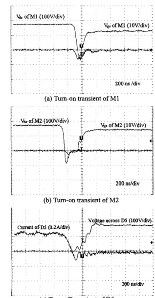
The waveforms of Fig.12 show that soft transition of the switches and the diodes is achieved in the proposed circuit. In Fig.12 (a), we could find that M1 is turned on after Vds drops to OV. Similar, Fig. 12(b) shows that M2 is turned on with ZVT. The turn-off transient of D5 is shown in Fig.12 (c). The voltage across D5 doesn’t rise until the current of D5 drops to zero. So we know that D5 is turned off naturally. Because the X-side and Y-side drivers are symmetric, we conclude that all the switches are operated with ZVT and all diodes are turned off naturally. \hs ofMl.(IOOV/div)
___l___l_j
. . . . . . . . . . . _ . . . . L 200nsldiv - I(a) Turn-on transient of M1
. . . . . . . . .
c ‘ .
. . .+. .;. . .:
]
. , . . . . . . V ~ S of M2 (€OOV/div) ~ \ % ~ o f M 2 (10V/div) . . . . . . . . . . . . . . . . . T . . . . . . . . .- (b) Turn-on transient of M2 . . . . . . . . ” . . . . . . . . . . . . . . . . . . . . . . . . . . . . . . . . . (c) Turn-off transient of D5Fig. 12 Soft transition of the switches and the diodes
Comparing the power consumption of these two driving circuits, we can find the effect of the energy recovery of the proposed circuit. Supplying the same DC bus voltage, 200 V, the average input current of the proposed circuit is 0.1OA and that of the simplest circuit is 0.14A. Therefore, about 30% energy is recovered by the proposed circuit.
VI. Conclusion
A regenerative driver for the PDP is proposed in this paper. It utilizes inductors to resonate with the equivalent intrinsic capacitance of PDP to avoid the abrupt charging/discharging operation. It not only achieves the energy recovery function but also perform the soft switching operation. All active switches are operated with zero voltage switching and all diodes are turned off naturally without the problem of reverse recovery. Comparing with prior approaches, the proposed sustain driving circuit is quite simple. The left side and right side circuits can be operated independently so it is not restricted to symmetrical operation and is suitable for practical applications. The presented circuit is experimentally verified to be applicable on an 8-inch plasma display
panel.
VII.
AcknowledgementThis work was supported in part by the National Science Council, Taiwan under the contract no. NSC87-2622-E002-015.
VU. Reference
[l] L. F. Weber, “Measurement of wall charge and capacitance variation for a single cell in AC plasma display panel,” IEEE Trans. on Electron Device, Vol. ED-24, No.7, pp. 533-538, November, 1997.
[2] L. F. Weber, K. W. Warren, “Power efficient sustain drivers and address drivers for plasma panel,” U. S. Patent, Number 4,866,349, Sep.
1989.
[3]T. Shinoda, “Method and a circuit for gradationally driving a flat display device”,
US.
Patent, Number 5,541,618, July, 1996.[4] M. Ohba, Y. Sano, “Energy recovery driver for a dot matrix ac plasma display panel with a parallel resonant circuit allowing power reduction,” U. S. Patent, Number 5,670,974, Sep. 1997.
[5]L. E Weber, M. B. Wood, “Energy recovery sustain circuit for the AC plasma display,” SID’87 Digest, pp. 92-95.
[6]A. Tanaka, “Low power driver circuit for AC plasma display panel,” U.S. Patent, Number 5,438,290, August, 1995.
[7] S . Y. Lin, C. L. Chen, C. C. Liu, K. Lee, “Lossless sustain driver for plasma display panel,” Power Conversion and Intelligent Motion, NOmberg, Germany, Vo1.38, pp.675-679, May 26-28, 1998.