國 立 交 通 大 學
光電工程學系碩士班
碩
士
論
文
非晶/結晶矽量子點埋入式氧化鋅薄膜
之開發與於光伏元件之應用
Development of amorphous- and crystalline-Si quantum dots
embedded ZnO thin films for photovoltaic device application
研 究 生:劉權政
指導教授:李柏璁 博士
非晶/結晶矽量子點埋入式氧化鋅薄膜
之開發與於光伏元件之應用
Development of amorphous- and crystalline-Si quantum dots
embedded ZnO thin films for photovoltaic device application
研 究 生:劉權政 Student:Chaun-Cheng Liu
指導教授:李柏璁 博士 Advisor:Dr. Po-Tsung Lee
國 立 交 通 大 學
光電工程學系碩士班
碩 士 論 文
A Thesis
Submitted to Department of Photonic and Institute of Electro-Optical Engineering College of Electrical Engineering and Computer Science
National Chiao Tung University In partial Fulfillment of the Requirements
for the Degree of Master in
Department of Photonic and Electro-Optical Engineering October 2012
Hsinchu, Taiwan, Republic of China
I
非晶/結晶矽量子點埋入式氧化鋅薄膜
之開發與於光伏元件之應用
研 究 生:劉權政
指導教授:李柏璁 博士
國立交通大學光電工程學系碩士班
摘要
近年來,由於矽量子點薄膜具有可大範圍調控能隙與獨特的光學特性,故已 被廣泛研究並應用於多種熱門光電元件,其中於光伏元件之應用亦被視為相當具 有潛力的研究之一,因其將可解決目前全矽基組成太陽能電池於短波長波段具有 較大能量損耗的問題。目前矽量子點薄膜主要以矽相關介電材料為矩陣材料,雖 已驗證其具有明顯光伏特性,但其特性仍受限於矩陣材料的高阻值特性,導致整 體光電效益尚無法達到預期。有鑒於目前矽量子點薄膜應用太陽能電池所遭遇的 瓶頸,我們提出以氧化鋅為矽量子點矩陣材料,因其不但具有矩陣材料所需必備 的寬能隙特性,同時更具有高光穿透度與高度可調的電性特性,故若能成功整合 矽量子點與氧化鋅薄膜,必可大幅提升矽量子點薄膜整合於太陽能電池的光電效 益。此篇論文中,我們利用射頻濺鍍薄膜沉積方式,成長二十週期的[氧化鋅/矽] 多層膜結構,藉由一高矽濺鍍功率與矽薄層厚度調控,於室溫下沉積出自組織矽 量子點埋入式氧化鋅薄膜,並分析該薄膜於不同退火溫度下,其結晶特性、光學 特性與電性特性。此外,我們亦利用調控適當的退火時間與氫退火製程,分別針 對非晶與結晶矽量子點薄膜做更進一步的光電特性優化,未來若能有效整合矽量 子點薄膜與非晶/微晶矽薄膜,將可邁向全矽基組成之高效率與低成本的第三代 薄膜太陽能電池。II
Development of Amorphous- and Crystalline-Si Quantum Dots
Embedded ZnO Thin Films for Photovoltaic Device Application
Student : Chuan-Cheng Liu
Advisor : Prof. Po-Tsung Lee
Department of Photonics and Institute of Electro-Optical Engineering,
National Chiao Tung University
Abstract
Recently, the silicon quantum dot (Si QD) thin films have been extensively studied and applied to the popular optoelectronics due to the widely tunable bandgap and unique optical properties. For example, the Si QD thin films have the great potential for photovoltaic (PV) applications because it can solve the optical loss problem in the short-wavelength range for the Si-based solar cells (SCs). So far, the Si-based dielectric materials are used as the matrix material of Si QD, and the PV properties has been demonstrated. However, the overall PV properties are still limited by the naturally high resistance of the Si-based dielectric matrix materials. In order to solve the bottleneck of the Si QD thin films applying to SC application, we propose to use ZnO as the matrix material of Si QDs since the ZnO thin film is a semiconductor material with wide bandgap, high transparency, and tunably electrical properties. These advantages are potential in improving the electro-optical properties of the Si QD thin films for SC application. In this study, the Si QD embedded ZnO thin films are fabricated by sputtering method and deposited by a [ZnO/Si] multilayer structure with 20 pairs. The self-assembled Si nano-clusters are formed in ZnO matrix by high Si sputtering power and thin Si layer thickness during deposition. The crystalline, optical, and electrical properties of the samples annealed at different temperatures are investigated and discussed. Besides, the electro-optical properties of the amorphous- and crystalline-Si QD thin films are also further improved by tuning the annealing time and using the H2 annealing process. The all Si-based third generation solar cells
with high efficiency and low cost can be highly expected by integrating the Si QD embedded ZnO thin films and the a- or μc-Si thin films in the future.
III
Acknowledgement
兩年的研究生活倏忽即逝,轉眼已到編寫這段文字的時刻,這兩年中無論是 實驗的摸索與學習亦或生活中的笑顏與淚水都盡情的填滿我腦中的每一個記憶 空間,讓我經歷了一段深刻且豐富的人生體驗。 首先誠摯的感謝指導教授李柏璁老師兩年來悉心的指導與照顧,在書報討論 中學到研究所需技巧以及重要的研究心態,歷來種種皆使我獲益良多。感謝口試 委員劉伯村教授、孫建文教授和林國瑞教授在百忙之中抽空指導以及諸多建議, 使本論文更趨完整。 在此感謝實驗室所有夥伴陪伴、支持與指導: 感謝光揚學長不厭其煩的指出 我研究中的缺失,且總能在我迷惘時為我解惑。感謝贊博、岳哥、家揚、佐哥、 佳裕在實驗過程中給予我的寶貴意見。已畢業的學長姊們金剛、文齡、邱立勛、 林雋崴、呂紹平不論是操作機台或問題討論都有莫大的幫助。感謝 ping、小智、 哲嶢、開昊的支持與鼓勵,尤其感謝 ping 的大力協助,幫助我事半功倍。小幫 手陳酷哥當然也不能忘記,感謝你的幫忙及搞笑。也期望在未來的路途中,能將 所遭遇到的辛苦與挫折,轉化成前進的動力,繼續朝下一目標邁進。 最後,謹以此文獻給我摯愛的雙親。感謝我的家人,在這段時間裡,一直守 護著我,讓我能全心全意完成碩士學業。 劉權政。2012 年 11 月 謹誌於 國立交通大學IV
Content
摘要... I Abstract ... II Acknowledgement ... III Content ... IV List of Figure... VI List of Table ... X Chapter 1 Introduction ... 1 1.1 Background ... 11.2 Limitation of Solar Cell Efficiency ... 2
1.3 Principle of Si QD Thin Film ... 4
1.4 Si QD Embedded in Dielectric Matrix Materials ... 6
1.5 Motivation ... 9
1.6 Characteristic of ZnO Material ... 10
Chapter 2 Sample Fabrication and Equipment ... 11
2.1 Sample Fabrication ... 11
2.1.1 Substrates Clean ... 11
2.1.3 Thin Film Deposition ... 11
2.1.4 Post-Annealing Process ... 12 2.1.5 Electrode Deposition ... 13 2.2 Equipment ... 14 2.2.1 AFM Image ... 14 2.2.2 SEM Image ... 15 2.2.3 TEM Image ... 16 2.2.4 Raman Spectrum ... 18
V
2.2.5 XRD Pattern ... 20
2.2.6 UV-Vis-NIR Spectrum ... 23
2.2.7 I-V Curve ... 23
Chapter 3 Results and Discussions ... 25
3.1 [ZnO/Si] Multilayer Thin Films ... 25
3.1.1 Structural Properties... 25
3.1.2 Crystalline Properties of Si QDs ... 26
3.1.3 Crystalline Properties of ZnO Matrix ... 28
3.1.4 Film Stress ... 30
3.1.5 Optical Properties... 31
3.1.6 Electrical Properties ... 32
3.2 a-Si QDs embedded ZnO thin films ... 36
3.2.1 Crystalline Properties ... 36
3.2.2 Electrical Properties ... 37
3.3 a-Si QDs embedded ZnO thin films with H2 annealing ... 39
3.3.1 Crystalline and Optical Properties ... 39
3.3.2 Electrical Properties ... 40
3.4 c-Si QDs embedded ZnO thin films ... 42
3.4.1 Crystalline Properties ... 42
3.4.2 Electrical Properties ... 43
3.5 c-Si QDs embedded ZnO thin films with H2 annealing ... 45
3.5.1 Crystalline and Optical Properties ... 45
3.5.2 Electrical Properties ... 46
Chapter 4 Conclusion ... 48
VI
List of Figure
Chapter 1
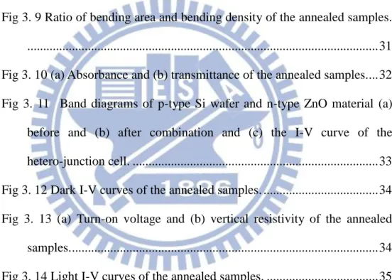
Fig 1. 1 Classification of three generation solar cells and its cost per peak watt
($/Wp). [5] ... 1 Fig 1. 2 Energy loss mechanisms of a single pn junction Si solar cell. ... 2 Fig 1. 3 Formation of energy levels from quantum confinement effect. ... 4 Fig 1. 4 Relation between the effective bandgap and QD size by using SiO2
and Si3N4. [9] ... 5
Fig 1. 5 Formation of nc-Si QDs embedded in the Si-based dielectric matrix
materials by a multilayer thin film structure. ... 6 Fig 1. 6 Bulk band diagram between crystalline silicon and its carbide, nitride
and oxide matrix. ... 7 Fig 1. 7 Schemes of the p-i-n Si QD thin film solar cell. ... 7 Fig 1. 8 I–V characteristics of the p-i-n Si QD thin film solar cell under 1-sun
illumination. ... 8 Fig 1. 9 Optical and electrical properties of ZnO material: (a) absorption
coefficient, (b) transmittance, (c) resistivity, (d) mobility, and (e) carrier
concentration. ... 10
Chapter 2
Fig 2. 1 Fabrication flow of the Si QD thin films. ... 11 Fig 2. 2 Diagram of ZnO/Si ML thin film structure. ... 12 Fig 2. 3 Illustration of the as-deposited and annealed [ZnO/Si] ML thin films.
VII
Fig 2. 4 Diagrams of (a) the square mask for the front electrode and (b) the
device structure. ... 13
Fig 2. 5 Illustration of scanning method by AFM. ... 14
Fig 2. 6 Image of the cantilever tip for AFM measurement. [20] ... 14
Fig 2. 7 Diagram of interaction between incident electron beam and sample. ... 15
Fig 2. 8 Imaging principle of phase contrast... 16
Fig 2. 9 Diffraction pattern of face-centered cubic (fcc) crystal. ... 16
Fig 2. 10 Imaging methods of diffraction contrast: (a) bright field image and (b) dark field image. ... 17
Fig 2. 11 (a) Bright field image and (b) dark field image of a BF+ ion implantation sample. ... 17
Fig 2. 12 Energy transfer of Raman effect. ... 18
Fig 2. 13 Diagram of Raman energy transition. ... 19
Fig 2. 14 Diagram of Bragg's diffraction. ... 21
Fig 2. 15 Diagram of θ-2θ scanning method. ... 22
Fig 2. 16 Diagram of grazing incident X-ray diffraction. ... 22
Chapter 3
Fig 3. 1 Surface morphologic images of the as-deposited ZnO (5 nm) and ZnO(5 nm)/Si(3 nm) thin films by AFM. ... 25Fig 3. 2 (a) Low magnification and (b) high magnification HRTEM images of the as-deposited [ZnO/Si] ML thin films. ... 26
Fig 3. 3 Raman spectra of the annealed ML thin films under different annealing temperature for 30 minutes... 27
VIII
Fig 3. 5 (a) Crystallinity and integrated intensity and (b) FWHM and peak
position for the nc-Si QDs from Raman spectra. ... 28 Fig 3. 6 XRD patterns of the annealed ML samples. Inset shows the XRD
pattern from 20 to 60o for sample F300. ... 29 Fig 3. 7 Integrated intensities of the normal, stressed, and total ZnO(002) for
the annealed samples... 30 Fig 3. 8 SEM images of the samples annealed at (a) 500oC and (b) 1000 oC for 30min. ... 31 Fig 3. 9 Ratio of bending area and bending density of the annealed samples.
... 31 Fig 3. 10 (a) Absorbance and (b) transmittance of the annealed samples.... 32 Fig 3. 11 Band diagrams of p-type Si wafer and n-type ZnO material (a)
before and (b) after combination and (c) the I-V curve of the
hetero-junction cell. ... 33 Fig 3. 12 Dark I-V curves of the annealed samples. ... 34 Fig 3. 13 (a) Turn-on voltage and (b) vertical resistivity of the annealed
samples. ... 34 Fig 3. 14 Light I-V curves of the annealed samples. ... 35 Fig 3. 15 (a) Open circuit voltage and (b) short circuit current of the annealed
samples. ... 35 Fig 3. 16 (a) Raman spectra and (b) XRD patterns of the samples annealed at
500 oC under different annealing time. ... 37 Fig 3. 17 (a) Dark and (b) light I-V curves of the samples annealed at 500 oC under different annealing time. ... 38 Fig 3. 18 (a) Raman spectra and (b) XRD patterns of the annealed samples
IX
after N2 and H2 annealing. ... 40
Fig 3. 19 (a) Absorbance and (b) transmittance of the annealed samples after
N2 and H2 annealing. ... 40
Fig 3. 20 (a) Dark and (b) light I-V curves of the annealed samples after N2
and H2 annealing. ... 41
Fig 3. 21 (a) Raman spectra and (b) XRD patterns of the samples annealed at
700 oC under different annealing time. ... 42 Fig 3. 22 Film bending density of the samples annealed at 700 oC under different annealing time. ... 43 Fig 3. 23 (a) Dark and (b) light I-V curves of the samples annealed at 700 oC under different annealing time. ... 44 Fig 3. 24 (a) Raman spectra and (b) XRD patterns of the annealed samples
after N2 and H2 annealing. ... 45
Fig 3. 25 (a) Dark and (b) light I-V curves of the samples after N2 and H2
X
List of Table
Table 1. 1 Energy loss simulation for 1.3 eV bandgap. [7] ... 3
Table 3. 1 Parameters for the crystalline properties of Si QDs under different
annealing temperature. ... 28 Table 3. 2 Crystalline properties of ZnO(002) for the annealed samples. ... 30 Table 3. 3 Curve-fitting results for the crystalline properties of ZnO matrix of
the samples annealed at 500 oC under different annealing time. ... 37 Table 3. 4 Parameters from I-V curves of the samples annealed at 500 oC under different annealing time. ... 38 Table 3. 5 Parameters from I-V curves of the annealed samples after N2 and
H2 annealing. ... 41
Table 3. 6 Curve-fitting results from XRD patterns of the samples annealed at
700 oC under different annealing time. ... 43 Table 3. 7 Parameters from I-V curves of the annealed samples at 700 oC under different annealing time. ... 44 Table 3. 8 Curve-fitting results from Raman spectra and XRD patterns of the
annealed samples after N2 and H2 annealing. ... 46
Table 3. 9 Parameters from I-V curves of the annealed samples after N2 and
1
Chapter 1 Introduction
1.1 Background
Recently, the green energy requirements are substantially increased due to the
environment population and the technology development, and solar cell is one kind of
the important green energies. The solar cells can be classified into three types, as
shown in Fig 1. 1. The first generation solar cells are high efficiency and high cost like
the c-Si bulk solar cell. Second generation solar cells are low cost and low efficiency
like the organic solar cell. The present limitation of solar cells is about 40% and their
costs per watt are still surcharge.[1] Therefore, the third generation solar cells with high
efficiency and low cost are needed like the dye-sensitized solar cell and the tandem
solar cell.[2-4]. It has the higher efficiency limitation about 60% and the cost is
expected to be lower than 0.5 $/W. The nano-crystalline Si quantum dot thin films with
tunably effective bandgap and good optical properties are great potential for the third
generation solar cell application.
2
1.2 Limitation of Solar Cell Efficiency
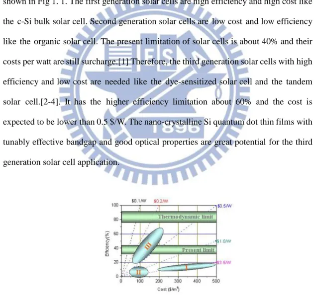
Fig 1. 2 shows the energy loss mechanisms of a single pn junction Si solar cell.
Such as the (1) thermalization loss, (2) junction voltage loss, (3) recombination loss,
and (4) contact voltage loss. The larger energy of incident light than Si bandgap will
lead to the obvious thermalization loss and limit the highest conversion efficiency
<44%, hence, it’s one of the critical energy loss mechanisms. We can cascade different
bandgap materials to decrease thermal loss. Recombination loss is also an important
loss mechanism and we can choose long life-time photo-excited carrier and perfect
lattice material to decrease it. Shockley and Queisser explore the relation of ideal solar
cell emission and blackbody radiation and the 1.3 eV bandgap of solar cell that has 31%
conversion is derived. [6] The 31% conversion is lower than previous 44% efficiency
because the lower output voltage is limited by junction voltage loss and contact voltage
loss. Output voltage is lower than theoretical energy bandgap. We can decrease
junction voltage loss and contact voltage loss to improve efficiency by condensing
sunlight.
Fig 1. 2 Energy loss mechanisms of a single pn junction Si solar cell.
From above discussion, junction voltage loss, contact voltage loss and
3
improvement is difficult. Table 1. 1 shows energy loss simulation of 1.3eV bandgap.
Thermal loss is a major loss in Table 1. 1 and it needs different bandgaps to decrease
thermalization loss. For Si material, the bandgap of different type Si material is
between 1.12 and 1.7eV. To further decrease thermal loss, the higher bandgap is needed.
So, Si quantum dot (QD) technology is proposed to reach higher bandgap of Si-based
solar cell.
4
1.3 Principle of Si QD Thin Film
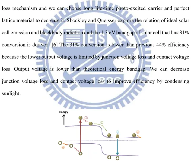
A narrow definition of quantum dots scales is less than 10 nanometers of the
zero-dimensional dots. The electrons and holes are confined in a tiny three-dimensional
energy barrier when the crystal bulk size reduces below de Broglie wavelength of free
electrons. In addition, quantum dot is formed by a few atoms and its electronic density
of states is between atoms and bulk due to quantum confinement effect. In Fig 1. 3,
quantum confinement leads discontinuous electron energy level that is similar with
atomic structure. Therefore, the physical properties of the quantum dots are different
from the macroscopic nature. [8] The electronic density of state changes with the dot
size, and that will affect its optical, electrical, and magnetic properties.
Fig 1. 3 Formation of energy levels from quantum confinement effect.
According to the quantum confinement effect, the nc-Si QD thin film can achieve
the larger effective bandgap than a-Si. In addition, it’s highly tunable by tuning the QD
size. Fig 1. 4 shows the effective bandgap increasing with decreasing QD size in SiO2
and Si3N4 matrixes. So, it demonstrates the possibility on tunable Si bandgap by Si QD.
The multi-junction Si-based solar cells with optimized light absorption can be reached
5
6
1.4 Si QD Embedded in Dielectric Matrix
Materials
The effective bandgap of Si can be largely tuned by using a QD nano-structure.
Therefore, the Si QD thin film has potential for LED, memory device, photovoltaic
applications and so on. [10, 11] So far, Si QDs are developed by using the Si-based
SiO2, Si3N4 and SiC matrix materials. The Si precipitation mechanism can be expressed
as equation (1-1) [12]:
Si(O, N, C)X→ (2x) Si(O2, N4/3, C) + (1 −X2)Si (1-1)
The thickness and composition of Si-rich layers are important parameters to tune
the QD size in a multilayer thin film structure. In figure 1.6, two materials are
repeatedly deposited to form the multilayer structure and the Si-rich atoms are
precipitated to form Si QDs during annealing process.
Fig 1. 5 Formation of nc-Si QDs embedded in the Si-based dielectric matrix materials by a multilayer thin film structure.
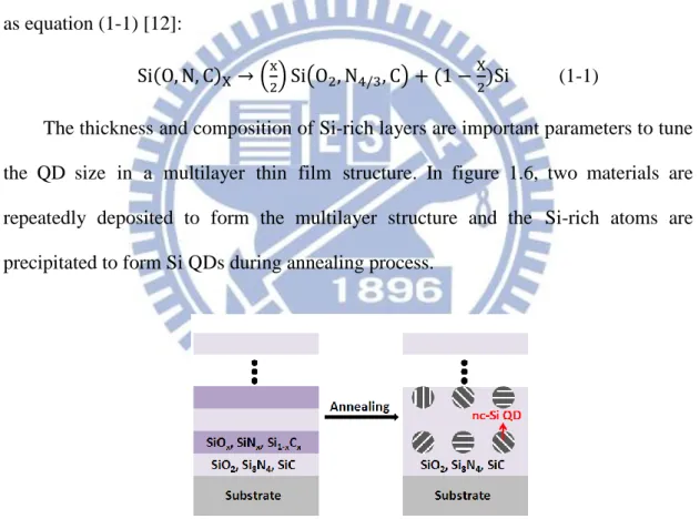
Fig 1. 6 shows the bulk band diagram between crystalline silicon and its carbide,
nitride, and oxide matrices. The tunneling probability is largely dependent on the
7
carrier transport efficiency of the QD thin films.
Fig 1. 6 Bulk band diagram between crystalline silicon and its carbide, nitride and oxide matrix.
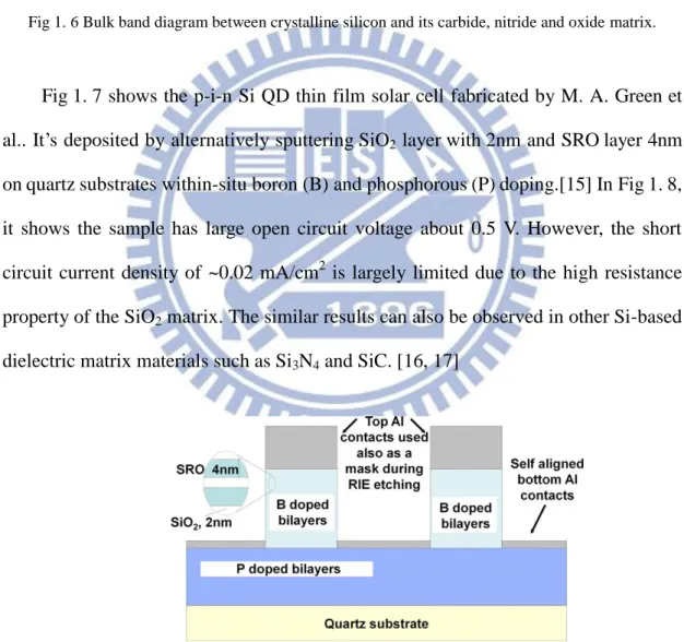
Fig 1. 7 shows the p-i-n Si QD thin film solar cell fabricated by M. A. Green et
al.. It’s deposited by alternatively sputtering SiO2 layer with 2nm and SRO layer 4nm
on quartz substrates within-situ boron (B) and phosphorous (P) doping.[15] In Fig 1. 8,
it shows the sample has large open circuit voltage about 0.5 V. However, the short
circuit current density of ~0.02 mA/cm2 is largely limited due to the high resistance property of the SiO2 matrix. The similar results can also be observed in other Si-based
dielectric matrix materials such as Si3N4and SiC. [16, 17]
8
9
1.5 Motivation
The Si QD thin films with tunable bandgap and good optical properties are great
potential in resolving the thermalization loss in the Si-based SC. However, the
Si-based dielectric matrix materials will obviously limit the carrier transport
efficiency and reduce the device’s performance due to their high resistance properties.
In order to efficiently improve those problems, we propose to use ZnO as matrix
material because ZnO has many suitable properties, such as wide bandgap and high
transparency like Si-based dielectric matrices. In addition, it’s also a semiconductor
with tunable electrical properties. Hence, it has great potential in improving the
conductivity than using the Si-based dielectric matrices and efficiently enhancing the
10
1.6 Characteristic of ZnO Material
ZnO thin film is a Ⅱ-Ⅵ semiconductor material. The wurtzite structure has a
hexagonal unit cell with two lattice parameters a and c in the ratio of c/a = 1.633. It has
wide bandgap about 3.2~3.4 eV and high transparent, as shown in Fig 1. 9 (a) and (b).
Fig 1. 9 (c)~(e) also shows the good electrical properties of resistivity, mobility, and
carrier concentration.[18] In addition, the n-type ZnO/ p-type Si hetrojunction solar cell
had also been studied by other groups.[19]
Fig 1. 9 Optical and electrical properties of ZnO material: (a) absorption coefficient, (b) transmittance, (c) resistivity, (d) mobility, and (e) carrier concentration.
11
Chapter 2 Sample Fabrication and
Equipment
2.1 Sample Fabrication
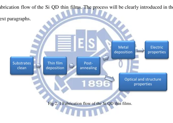
The sample preparation process is introduced in this chapter, Fig 2. 1 shows a brief
fabrication flow of the Si QD thin films. The process will be clearly introduced in the
next paragraphs.
Fig 2. 1 Fabrication flow of the Si QD thin films.
2.1.1 Substrates Clean
The Si wafer is chemically etched with the solutions of H2SO4:H2O2 = 4:1 at 75°C
for 15 minutes and HF:H2O = 25:1200 at room temperature for 2 minutes in sequence.
The quartzes were ultrasonically cleaned with acetone and alcohol for 10 minutes.
2.1.3 Thin Film Deposition
The radio-frequency (RF) magnetron sputtering method is used to deposit the
Substrates clean Thin film deposition Post-annealing Metal deposition Electric properties
Optical and structure properties
12
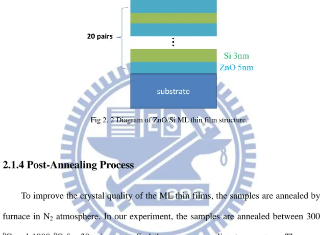
ZnO/Si multilayer (ML) thin films. ZnO and Si thin-layers are alternately deposited to
form the ML structure, as shown in Fig 2. 2. The base and working pressures are 8*10-7 torr and 5*10-3 torr. The sputtering powers of ZnO and Si are fixed at 75 W and 110 W, and the thicknesses are deposited for 5 nm and 3 nm, respectively.
Fig 2. 2 Diagram of ZnO/Si ML thin film structure.
2.1.4 Post-Annealing Process
To improve the crystal quality of the ML thin films, the samples are annealed by
furnace in N2 atmosphere. In our experiment, the samples are annealed between 300 o
C and 1000 oC for 30 minutes to find the proper annealing temperature. Then, we change the annealing time between 30 minutes and 2hr when the proper annealing
temperature is selected. Finally, the samples with better electro-optical characteristics
13
Fig 2. 3 Illustration of the as-deposited and annealed [ZnO/Si] ML thin films.
2.1.5 Electrode Deposition
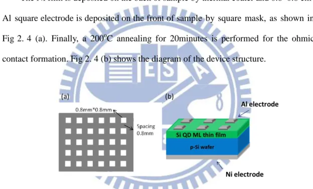
The Ni film is deposited on the back of sample by thermal coater and 0.8*0.8 cm2 Al square electrode is deposited on the front of sample by square mask, as shown in
Fig 2. 4 (a). Finally, a 200oC annealing for 20minutes is performed for the ohmic contact formation. Fig 2. 4 (b) shows the diagram of the device structure.
14
2.2 Equipment
2.2.1 AFM Image
The surface morphologies are analyzed by a Digital Instrument D3100 atomic
force microscopy (AFM) since it can scan the nano-scaled surface. Generally, there
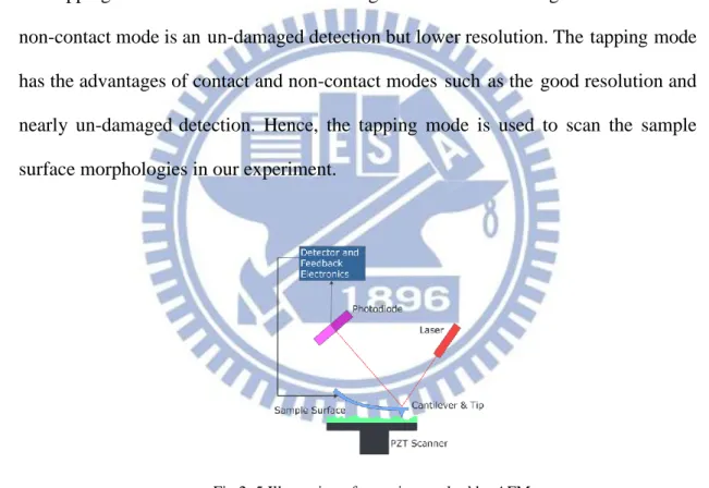
are three scanning modes by using AFM including contact mode, non-contact mode
and tapping mode. The contact mode is a high resolution but damaged detection. The
non-contact mode is an un-damaged detection but lower resolution. The tapping mode
has the advantages of contact and non-contact modes such as the good resolution and
nearly un-damaged detection. Hence, the tapping mode is used to scan the sample
surface morphologies in our experiment.
Fig 2. 5 Illustration of scanning method by AFM.
15
2.2.2 SEM Image
The scanning electron microscope (SEM) is one of electron microscopes, it uses a
focused high-energy electron beam to produce varied signals at the sample surface. The
signals produced by the interacting electrons containing the useful information such as
the shape, atomic structure, and conductivity. Fig 2. 7 shows the interaction between
incident electron beam and sample. When an electron hits the surface, it may be
reflected (backscattered), absorbed, or conducted away. The atoms become unstable,
give off another electron (a secondary electron), or to give off light in order to stabilize
when the atoms absorb electrons. Backscattered electrons and secondary electrons are
produced at the surface of sample and SEM can collect these electrons to gain the
surface morphology of samples. [20] In the lower conductive samples, the electron
beam possibly causes the accumulating charges on the surface to decrease the image
resolution, hence, the ultra-thin Au layer is coated to eliminate the accumulating
charges in our experiment.
16
2.2.3 TEM Image
The transmission electron microscopy (TEM) is a microscopy technique using a
tunneling electron beam through an ultra-thin specimen and interacting with the sample.
An image is formed from the interaction of the electrons transmitted through the sample.
The image is magnified and focused onto an imaging device, such as a fluorescent
screen, on a layer of photographic film, or to be detected by a sensor such as a CCD
camera. There are two ways of TEM images including phase contrast and diffraction
contrast. Fig 2. 8 shows the imaging principle of phase contrast. [20] Direction electron
beam and diffraction electron beam are combined by lens to form phase contrast image.
Phase contrast image is different with crystal structure of sample. Fig 2. 9 shows the
diffraction pattern of face-centered cubic (fcc) structure.
Fig 2. 8 Imaging principle of phase contrast.
17
Diffraction contrast can be classified to bright field image and dark field image.
Fig 2. 10 shows the imaging principle of diffraction contrast. In Fig 2. 10 (a),
diffraction electron beam is screened by object aperture, the bright field image is
formed by direct electron beam. Fig 2. 10 (b) shows the principle of dark field image,
the dark field image is formed by diffraction electron beam. The name of bright and
dark field images originate from the high contrast of images. Fig 2. 11 shows the
bright and dark field images of BF+ ion implantation.
TEM is capable of imaging at a significantly higher resolution than optical
microscopes owing to the smaller de Broglie wavelength of electrons. This enables the
instrument's user to examine fine detail—even as small as a single column of atoms,
which is tens of thousands times smaller than the smallest resolvable object in a light
microscope.
Fig 2. 10 Imaging methods of diffraction contrast: (a) bright field image and (b) dark field image.
18
2.2.4 Raman Spectrum
The Raman effect occurs when light impinges upon a molecule and interacts with
the electron cloud and the bonds of that molecule. The momentum and energy maybe
change when photon collide molecule. The former changes light propagation direction
also called Rayleigh scattering. The latter is called Raman scattering when light energy
changes after collision. Fig 2. 12 shows the principle of Raman Effect. [20] The relation
between Raman shift (∆σ) and energy change (∆E) is shown as equation (2-1): ∆σ = σ (laser enegy) – σ’ (scattered light energy)
= ∆E/hc (2-1),
where h is Planck constant and c is light velocity.
Fig 2. 12 Energy transfer of Raman effect.
For the spontaneous Raman effect, which is a form of light scattering, a photon
excites the molecule from the ground state to a virtual energy state. When the molecule
relaxes it to emit a photon, it returns to a different rotation or vibration state. The energy
difference between the original state and the new state leads to a shift in the emitted
photon's frequency away from the excitation wavelength. If the final vibrational state of
the molecule is more energetic than the initial state, then the emitted photon will be
19
shift in frequency is designated as a Stokes shift. If the final vibrational state is less
energetic than the initial state, then the emitted photon will be shifted to a higher
frequency, and this is designated as an Anti-Stokes shift. Raman scattering is an
example of inelastic scattering because of the energy transfer between the photons and
the molecules during their interaction. Fig 2. 13 shows the diagram of Raman energy
transition.
Fig 2. 13 Diagram of Raman energy transition.
In our experiment, the crystalline properties of Si QDs are confirmed by the
Raman spectrum examined by a 488 nm diode-pumped solid-state (DPSS) laser
(HOROBA, Lab RAM HR). The focused spot size is about 2 um in diameter, and the
20
2.2.5 XRD Pattern
X-ray diffraction (XRD) is a non-destructively analytical techniques which can
reveal the crystal structure, chemical composition, and physical properties of materials.
These techniques are based on observing the diffraction intensity of an X-ray beam
hitting a sample as a function of incident and diffracted angle, polarization, and
wavelength or energy.
Crystals are regular arrays of atoms, and X-rays can be considered waves of
electromagnetic radiation. Atoms scatter X-ray waves, primarily through the atoms'
electrons. Just as an ocean wave striking a lighthouse produces secondary circular
waves emanating from the lighthouse, so an X-ray striking an electron produces
secondary spherical waves emanating from the electron. This phenomenon is known as
elastic scattering, and the electron (or lighthouse) is known as the scatter. [20] A regular
array of scatters produces a regular array of spherical waves. Although these waves
cancel one another out in most directions through destructive interference, they add
constructively in a few specific directions, determined by Bragg's law:
2dsinθ = nλ (2-2), Here d is the spacing between diffracting planes, θ is the incident angle, n is any integer, and λ is the wavelength of the beam. Fig 2. 14 shows the diagram of Bragg's law. These specific directions appear as spots on the diffraction pattern called
reflections. Thus, X-ray diffraction results from an electromagnetic wave (the X-ray)
impinging on a regular array of scatters (the repeating arrangement of atoms within the
21
Fig 2. 14 Diagram of Bragg's diffraction.
Generally, grain size increases with decreasing FWHM. The larger grain size, the
better electrical property is. The equation of calculating the grain size is shown as:
Grain size = 0.94 ∗d∗sinɵλ (2-3), here d is spacing between crystal plane.
For XRD measurement, the common methods are phase analysis (θ-2θ analysis) and grazing incident X-ray diffraction (GIXRD). Fig 2. 15 shows the diagram of θ-2θ analysis. The phase of bulk materials, thin films and powder samples is identified by
the light source generates and receiver movement at different angles. For thin film
samples, if the skin depth of X-ray was thicker than thin film, the signal of sample
would be mainly from substrate. So, GIXD is used to measure thin film samples. Fig 2.
16 shows the diagram of grazing incident X-ray diffraction. The incident X-ray angle
with thin film is fixed at very small degree and detector collects signal at different
angles. This way can increase the interaction area between thin film and X-ray to
enhance the signal of thin film. In our experiment, the X-ray diffraction patterns of ML
sample is measured by GIXD with 2o incident angle and the system is Bede-D1 X-ray diffractometer (XRD) with Cu Kα radiation (λ = 1.5418 Ǻ).
22
Fig 2. 15 Diagram of θ-2θ scanning method.
23
2.2.6 UV-Vis-NIR Spectrum
Ultraviolet-visible-near infrared spectroscopy (UV-Vis-NIR) refers to absorption
spectroscopy or reflectance spectroscopy in the UV-Vis-NIR region. The absorption or
reflectance in the visible range directly affects the perceived color of the chemicals
involved. The absorbance and reflectance are measured by UV-Vis-NIR and then
absorption coefficient could be derived from α=A/d, here A is the absorbance of
materials and d is the film thickness. The optical characteristic of materials can be
classified to direct and indirect bandgap. The equation of effective optical bandgap is
shown below:
(αhv)γ = B(hv − Egopt) (2-4),
where h is Planck’s constant, v is the frequency of the radiation, and B is the edge width
parameter. The value of γ is dependent on the Egopt behavior, such as γ=2 for direct
Eg,opt and γ=1/2 for indirect Egopt. In our experiment, indirect bandgap is used to
calculate optical bandgap. The reflection and transmittance spectra are measured by a
Hitachi U-4100.
2.2.7 I-V Curve
The electrical properties of p-n junction between thin film and Si wafer can be
understood by I-V characteristics. In addition, we can use I-V characteristics to
estimate the vertical resistivity from the linear trend line in the high bias region. We
can calculate the resistivity by combining the resistance as equation (2-5):
24
where ρ is the resistivity, A is the cross-sectional area, and L is the length. The
cross-sectional area can be split into the width W and the thickness t. In our experiment,
the I-V curves are measured by using a E5270B 8-slot precision measurement
mainframe (Agilent Technologies), and a halogen lamp with power density of ~20
25
Chapter 3 Results and Discussions
3.1 [ZnO/Si] Multilayer Thin Films
The annealing temperature is important for the crystallization of Si QDs and ZnO
matrix, therefore, the [ZnO/Si] ML thin films were annealed from 300 to 1000 oC for 30 minutes. The crystalline, electrical, and optical properties of the [ZnO/Si] ML thin
films under different annealing temperature are discussed here.
3.1.1 Structural Properties
The surface morphologic images of the as-deposited ZnO (5 nm) and ZnO(5
nm)/Si(3 nm) thin films by AFM are shown in Fig 3. 1, the self-assemble Si
nano-clusters are clearly formed on ZnO thin-layer. To further confirm the formation
of Si nano-clusters, the high resolution transmission electron microscopy (HRTEM)
images are also examined, as shown in Fig 3. 2. It indicates the clear ML structure and
the self-assembled a-Si nano-clusters with size range from 2 to 5 nm. Hence, we
demonstrate that the self-assembled a-Si nano-clusters can be formed by a [ZnO/Si]
ML deposition structure with a high Si sputtering power.
Fig 3. 1 Surface morphologic images of the as-deposited ZnO (5 nm) and ZnO(5 nm)/Si(3 nm) thin films by AFM.
26
Fig 3. 2 (a) Low magnification and (b) high magnification HRTEM images of the as-deposited [ZnO/Si] ML thin films.
3.1.2 Crystalline Properties of Si QDs
From literatures, Raman spectrum of the Si QD thin films can be decomposed
into three components with peaks located at ~480, 500~510, and 510~520 cm-1, which are contributed from the transverse optical (TO) modes of Si-Si vibrations in the
amorphous (a-Si), intermediate (i-Si), and nano-crystalline (nc-Si) phases of Si
respectively. [21] Hence, the Raman spectra of the annealed samples under different
annealing temperature are performed to understand the variation of the crystalline
properties of Si QDs, as shown in Fig 3. 3, the nc-Si signals are clearly observed in
samples annealed at higher than 600 oC. The curve-fitting result of sample F1000 is also confirmed, as shown in Fig 3. 4, it shows the well matched result with the
27
Fig 3. 3 Raman spectra of the annealed ML thin films under different annealing temperature for 30 minutes.
Fig 3. 4 The curve-fitting result of Raman spectrum for sample F1000.
The parameters of the curve-fitting results from Raman spectra are shown in
Table 3. 1, the corresponding plots are shown in Fig 3. 5. Here the Si crystallinity (CSi)
is estimated by equation (3-1) as below:
Si Crystallinity (%) = Inc+Ii
Inc+Ii+Ia× 100% ( 3-1 ),
where Inc, Ii and Ia are the integrated intensities of a-Si, i-Si, and nc-Si peaks. With
increasing the annealing temperature, the increased CSi and integrated intensity and
28
crystalline quality of Si QDs.
Table 3. 1 Parameters for the crystalline properties of Si QDs under different annealing temperature.
Fig 3. 5 (a) Crystallinity and integrated intensity and (b) FWHM and peak position for the nc-Si QDs from Raman spectra.
3.1.3 Crystalline Properties of ZnO Matrix
The crystalline property of ZnO matrix has strong influences on the optical and
electrical properties of the ZnO thin films. [22]Fig 3. 6 shows the XRD patterns of the
annealed ML thin films, the c-axis (002) preferred orientation of ZnO matrix is clearly
observed. Inset of Fig 3. 6 shows the large range XRD scan from 20 to 60o for sample F300,there are no other crystallization signals observed. All annealed samples show
29
Fig 3. 6 XRD patterns of the annealed ML samples. Inset shows the XRD pattern from 20 to 60o for sample F300.
The XRD pattern of ZnO bulk locates at ~34.4o and the d-spacing value is about 2.60 Å . [23] The stress in ZnO thin film will affect characteristic of ZnO thin film.[24]
In our experiment, the crystalline signals of ZnO(002) have to be decomposed into
two components contributed from the normal and stressed ZnO crystals with peaks
located at ~34.4o and 35.5~36.7o individually. The curve-fitting results from XRD patterns are shown in Table 3. 2, and Fig 3. 7 shows the integrated intensity of the
normal, stressed, and total ZnO(002) crystals. Sample F500 has the largest residual
film stress since it shows the highest stressed intensity, it may be caused by the
increased amounts of ZnO(002) or a-Si from the phase separation of the silicon-rich
oxide (SiOx → Si + SiO2). In addition, the total ZnO(002) intensities of the samples
annealed over 500oC decrease with annealing temperature possibly due to the restriction from the phase transformation of Si QDs from a- to c-Si phases.
30
Table 3. 2 Crystalline properties of ZnO(002) for the annealed samples.
Fig 3. 7 Integrated intensities of the normal, stressed, and total ZnO(002) for the annealed samples.
3.1.4
Film Stress
Fig 3. 8 shows the SEM images of samples F500 and F1000 for 30 minutes, the
bended film is observed in sample F1000. Fig 3. 9 also shows the bending area ratio
and bending density of the annealed samples. It indicates the film bending problem
31
ratio clearly increase with increasing the annealing temperature. Comparing with the
crystalline properties of the Si QDs from Raman spectra, nc-Si signals are observed
from 600oC and also increased with increasing the annealing temperature. The crystal structure of ZnO is wurtzite and the crystal structure of Si is face-centered cubic
crystal structure. [25] Hence, it means the film bending problem comes from the
over-large film stress mainly due to the phase transformation of Si QDs from a- to
c-Si phases during annealing.
Fig 3. 8 SEM images of the samples annealed at (a) 500oC and (b) 1000 oC for 30min.
Fig 3. 9 Ratio of bending area and bending density of the annealed samples.
3.1.5 Optical Properties
32
samples. In the long-wavelength range, the samples annealed at ≦500 oC show the low T and high A due to more deficiencies from a-Si QDs, the samples annealed at
>600 oC show the low A and high T owing to the reduced deficiencies from the obvious nc-Si QDs formation. In addition, the highest absorbance of the sample
annealed at 500 oC is observed, it means that the stressed ZnO(002) leads to a larger defects formation than normal ZnO(002). The low A and high T observed in samples
annealed at >600 oC are the good results for tandem solar cell application because the upper cell of tandem solar cells needs to avoid the obvious light absorption in the
long-wavelength.
Fig 3. 10 (a) Absorbance and (b) transmittance of the annealed samples.
3.1.6 Electrical Properties
The band diagrams of p-type Si wafer and n-type ZnO thin films and the
corresponding I-V curve are shown in Fig 3. 11. Here the Fermi level of Si wafer
(Ef(Si)) from its conduction band is ~0.76 eV due to the doping concentration of ~1016
cm-3 used. Besides, according to literatures, we know the conduction band of Si is close to that of ZnO. [26]Hence, the combination of these two materials can form the
33
hetero-junction as a diode, and the turn-on voltage (Vt) is mainly influenced by the
Fermi level difference between both materials. In addition, since the Si QDs are
embedded in the ZnO matrix, it can be expected that the crystalline quality of Si QDs
may affect the effective Fermi level of thin films.
Fig 3. 11 Band diagrams of p-type Si wafer and n-type ZnO material (a) before and (b) after combination and (c) the I-V curve of the hetero-junction cell.
The dark I-V curves of the annealed samples are shown in Fig 3. 12. The samples
annealed at <500 oC shows the good I-V properties, however, the current orders are decreased in the samples annealed at >500 oC because of the film bending problem. The film bending regions will lead to the formations of open-circuit and interface
defect and limit the electrical transportation properties. Fig 3. 13 (a) shows the Vt of
the annealed samples from the dark I-V curves. To compare with the above results, the
increased Vt (a larger build-in electric field) from 600 oC is possibly resulted from the
improved crystalline quality of Si QDs or the film bending problem with increasing
the annealing temperature. Fig 3. 13 (b) shows the vertical resistivity from the dark
I-V curves, the samples annealed at ≦700 oC has the good resistivity with <105 Ω-cm, which are obviously lower than that of un-doped Si QDs using SiO2 matrix for
~108 Ω-cm. [27] The resistivity of samples annealed at ≧800 oC is largely increased due to the serious film bending problem.
34
Fig 3. 12 Dark I-V curves of the annealed samples.
Fig 3. 13 (a) Turn-on voltage and (b) vertical resistivity of the annealed samples.
Fig 3. 14 shows the light I-V curves of the annealed samples, here the result for
sample annealed at 1000 oC couldn’t be shown due to a charging effect. The corresponding open circuit voltage (VOC) and short circuit current (ISC) are also shown
in Fig 3. 15. In Fig 3. 15 (a), the trend of VOC is similar with Vt while increasing the
annealing temperature, hence, it means the increased Vt with increasing the annealing
temperature from 600 to 800 oC is mainly contributed from the increased crystallinity of Si QDs. The improved crystalline quality of Si QDs will lead to a higher effective
Ef(ZnO) and form a larger build-in electric field. In Fig 3. 15 (b), the ISC of samples
35
it may be caused by the increased residual film stress. When the annealing
temperature is higher than 500 oC, the ISC obviously increases with increasing the
annealing temperature and achieve the highest value at 700 oC due to the c-Si QDs formation. The ISC of sample annealed at 800 oC largely reduced by the high resistivity
owing to the serious film bending problem. Hence, the sample annealed at 700 oC has the better electro-optical properties for PV application.
Fig 3. 14 Light I-V curves of the annealed samples.
36
3.2 a-Si QDs embedded ZnO thin films
As the discussions in section 3.1, 500 oC is a critical annealing temperature without film bending problem observed. Although the ISC and VOC are reduced from
the high residual film stress, but it has the highest crystalline intensity of ZnO(002)
and low resistivity. Therefore, the sample annealed at 500 oC has the potential for further improvement on PV properties for the a-Si QD embedded ZnO thin films by
optimizing the annealing conditions. In this section, the properties of a-Si QD thin
films with and without H2 annealing will be discussed here.
3.2.1 Crystalline Properties
Fig 3. 16 (a) shows the Raman spectra of samples annealed at 500 oC for 30 minutes, 1 hour, and 2 hours. Similar a-Si signals are observed in these three samples.
The XRD patterns for the crystalline properties of ZnO matrix are shown in Fig 3. 16
(b), the ZnO(002) peaks can be well-fitted by the normal and stressed ZnO
components. Table 3. 3 show the curve-fitting results for the normalized integrated
intensity. The total ZnO(002) intensity is increased by increasing the annealing time,
and the stressed ZnO(002) intensity is reduced while the annealing time is longer than
1 hour. Hence, the sample annealed at 500 oC for 2 hours has the better crystalline properties of ZnO(002), and it indicates that the crystalline quality of ZnO matrix can
37
Fig 3. 16 (a) Raman spectra and (b) XRD patterns of the samples annealed at 500 oC under different annealing time.
Table 3. 3 Curve-fitting results for the crystalline properties of ZnO matrix of the samples annealed at 500 oC under different annealing time.
3.2.2 Electrical Properties
Fig 3. 17 shows the dark and light I-V curves of the samples annealed at 500 oC for 30 minutes, 1 hour and 2 hours, and the corresponding electrical parameters are
shown in Table 3. 4. The Vt, rectification, VOC, and ISC are improved by increasing the
annealing time, which are matched with the result of the total crystalline intensity of
ZnO(002). However, the ideal factors seems to be affected by the stressed ZnO(002)
intensity. The ideal factor larger than 2 is also observed in the Si QD thin films by
other group’s work, the cause had been demonstrated due to the trapping effect from defects. [28] Hence, the defect density in the a-Si QD embedded ZnO thin film is
38
dominated by the stressed ZnO(002) intensity.
Fig 3. 17 (a) Dark and (b) light I-V curves of the samples annealed at 500 oC under different annealing time.
Table 3. 4 Parameters from I-V curves of the samples annealed at 500 oC under different annealing time.
39
3.3 a-Si QDs embedded ZnO thin films with H
2annealing
In the Si QDs thin film references, the defects at the interface of Si QDs and
SRO can be eliminated by H2 annealing. [29] In the ZnO thin film references, the
defects can be eliminated by H2 annealing and H atom can be a better donor. [30, 31]
Therefore, we expect defects and quality of thin film can be improved after H2
annealing.
The sample annealed at 500 oC for 2 hours is chosen to be annealed in H2
environment for 1 hour and the annealing temperature is tried from 300 to 500 oC. The sample annealed at 500 oC in H2 shows the better PV properties; hence, here it is
compared with the reference sample annealed in N2 at 500 oC for 1 hour more.
3.3.1 Crystalline and Optical Properties
Fig 3. 18 (a) shows the Raman spectra of the annealed samples after N2 and H2
annealing, both samples show the similar a-Si signals. Fig 3. 18 (b) shows the XRD
patterns. The normalized integrated intensity of stressed ZnO(002) is clearly reduced
in H2 annealing (~3.4×10² a. u.) than that in N2 annealing (~2.7×10³ a. u.). It means
the crystalline quality of ZnO matrix can be efficiently improved by using a H2
annealing process.
The absorbance and transmittance of the annealed samples after N2 and H2
annealing are shown in Fig 3. 19. The absorbance and transmittance are obviously
improved in the long-wavelength range by H2 annealing due to the better crystalline
40
Fig 3. 18 (a) Raman spectra and (b) XRD patterns of the annealed samples after N2 and H2 annealing.
Fig 3. 19 (a) Absorbance and (b) transmittance of the annealed samples after N2 and H2 annealing.
3.3.2 Electrical Properties
Fig 3. 20 shows the dark and light I-V curves of the annealed samples after N2
and H2 annealing, and the corresponding parameters are shown in Table 3. 5. The ideal
factor of the sample annealed in H2 (~3.0) is lower than that in N2 (~4.5), which is
meaning the decreased defect density. From XRD results, it indicates that the
decreased defect density is contributed from the reduced intensity of stressed
ZnO(002) by H2 annealing. In addition, the photo-response properties including the
VOC and ISC are also clearly enhanced by H2 annealing. Therefore, we demonstrate
41
ZnO thin films can be efficiently improved by H2 annealing, and more enhancements
can be expected by optimizing the H2 annealing conditions.
Fig 3. 20 (a) Dark and (b) light I-V curves of the annealed samples after N2 and H2 annealing.
42
3.4 c-Si QDs embedded ZnO thin films
In section 3.1, the better PV properties of the c-Si QD embedded ZnO thin films
is observed at 700 oC. Hence, in this section, the properties of the c-Si QD embedded ZnO thin films are discussed and optimized by tuning the annealing time.
3.4.1 Crystalline Properties
Fig 3. 21 shows the Raman spectra and XRD patterns of the samples annealed at
700 oC for 30 minutes, 1 hour, and 2 hours, the corresponding parameters are shown
in Table 3. 6. The nc-Si signal is clearly observed in these three samples, and it shows
the higher Si crystallinity as increasing the annealing time. The stressed ZnO(002)
intensity is reduced when the annealing time is longer than 30 minutes, however, the
total ZnO(002) intensity is also decreased at the same time. It indicates that the longer
annealing time at 700 oC possibly decrease the crystalline quality of ZnO matrix for the c-Si QDs embedded ZnO thin films. Fig 3. 22 shows the film bending density of
the samples annealed at 700 oC under different annealing time, it indicates the film bending density doesn’t increase while increasing the annealing time at 700 o
C.
Fig 3. 21 (a) Raman spectra and (b) XRD patterns of the samples annealed at 700 oC under different annealing time.
43
Table 3. 6 Curve-fitting results from XRD patterns of the samples annealed at 700 oC under different annealing time.
Fig 3. 22 Film bending density of the samples annealed at 700 oC under different annealing time.
3.4.2 Electrical Properties
Fig 3. 23 shows the dark and light I-V curves of the samples annealed at 700 oC under different annealing time, and the corresponding parameters are shown in Table
3. 7. Here the ideal factors are larger than those of a-Si QD thin films because of the
film bending problem in the c-Si QD thin films, however, it’s also clearly affected by
the stressed ZnO intensity. As increasing the annealing time, the Vt and VOC
simultaneously increase may due to the higher Si crystallinity formation, however, it
also lead to the higher resistivity. Hence, it indicates the longer annealing time could
44
Fig 3. 23 (a) Dark and (b) light I-V curves of the samples annealed at 700 oC under different annealing time.
Table 3. 7 Parameters from I-V curves of the annealed samples at 700 oC under different annealing time.
45
3.5 c-Si QDs embedded ZnO thin films with H
2annealing
In this section, the crystalline, optical, and electrical properties of the c-Si QDs
embedded ZnO thin films after H2 annealing are discussed.
3.5.1 Crystalline and Optical Properties
Fig 3. 24 shows the Raman spectra and XRD patterns of the annealed samples
after N2 and H2 annealing, and the corresponding curve-fitting results are shown in
Table 3. 8. The crystalline properties of Si QDs are similar by N2 and H2 annealing
such as the crystallinity and FWHM values. However, the total intensity of ZnO(002)
is increased by H2 annealing, it means the H2 annealing process can also improve the
crystalline properties of ZnO matrix for the c-Si QDs embedded ZnO thin films.
46
Table 3. 8 Curve-fitting results from Raman spectra and XRD patterns of the annealed samples after N2
and H2 annealing.
3.5.2 Electrical Properties
Fig 3. 25 shows the dark and light I-V curves of the samples after N2 and H2
annealing, and the corresponding parameters are shown in Table 3. 9. The Vt,
resistivity, and rectification are obviously enhanced because of the improved quality
of ZnO matrix after H2 annealing. Besides, the ideal factor is also clearly reduced
after H2 annealing, which is meaning the decreased defect density. Hence, the Si QD
thin films after H2 annealing show the better photo-response properties due to the
improvement of crystalline properties of ZnO matrix.
47
48
Chapter 4 Conclusion
The Si QD embedded ZnO thin films had been successfully fabricated by using a
[ZnO/Si] ML structure. The resistivity of the Si QD embedded ZnO thin films
annealed at <700 oC is obviously lower than that using a SiO2 matrix. When the
annealing temperature is <500 oC, no crystalline Si signals are observed. The a-Si QD embedded ZnO thin films annealed for 30 minutes show the good ISC but low VOC.
When the annealing temperature is >600 oC, the crystalline Si signals can be observed. The c-Si QD embedded ZnO thin films show the good optical properties with the
high-T and low-A in the long-wavelength range. At the annealing temperature of 700
o
C for 30 minutes, the good ISC and VOC are simultaneously observed. However, the
film bending problem is also examined in the c-Si QD embedded ZnO thin films due
to the phase transformation of a- to c-Si QDs embedded in c-ZnO matrix.
For the a-Si QD embedded ZnO thin film, the residual film stress is reduced by
increasing the annealing temperature or using a H2 annealing process. The reduced
film stress can lead to the better optical properties and the lower defect density and
improve the PV properties. For the c-Si QD embedded ZnO thin films, the increased
annealing temperature reduces the residual film stress and slightly increases the Si
crystallinity, however, it also decreases the crystalline intensity of ZnO matrix. That
result makes the optimal annealing time for better PV properties is at 1 hour not 2
hours. More improvements of PV properties are also observed by using a H2
annealing process due to the enhanced crystalline intensity of ZnO matrix.
In the future, more enhancements on the PV properties of the Si QD thin films
can be expected by using the ZnO matrix material after resolving the largely residual
49
Reference
[1] M. Wiemer, V. Sabnis, and H. Yuen, "43.5% Efficient Lattice Matched Solar Cells," High and Low Concentrator Systems for Solar Electric Applications Vi, vol. 8108, 2011.
[2] L. Y. Han, A. Islam, H. Chen, C. Malapaka, B. Chiranjeevi, S. F. Zhang, X. D. Yang, and M. Yanagida, "High-efficiency dye-sensitized solar cell with a novel co-adsorbent," Energy & Environmental Science, vol. 5, pp. 6057-6060, 2012.
[3] S. H. Hong, Y. S. Kim, W. Lee, Y. H. Kim, J. Y. Song, J. S. Jang, J. H. Park, S. H. Choi, and K. J. Kim, "Active doping of B in silicon nanostructures and development of a Si quantum dot solar cell," Nanotechnology, vol. 22, 2011.
[4] S. Y. Lien, Y. C. Chang, Y. S. Cho, Y. Y. Chang, and S. J. Lee, "Deposition and Characterization of High-Efficiency Silicon Thin-Film Solar Cells by HF-PECVD and OES Technology," IEEE Transactions on Electron Devices, vol. 59, pp. 1245-1254, 2012.
[5] M. A. Green, "Third generation photovoltaics: Ultra-high conversion efficiency at low cost," Progress in Photovoltaics, vol. 9, pp. 123-135, 2001. [6] W. W. Shockley, "Elective Neck Dissection for Melanoma - the Great Debate," Southern Medical Journal, vol. 79, pp. 37-37, 1986.
[7] L. C. Hirst and N. J. Ekins-Daukes, "Fundamental losses in solar cells," Progress in Photovoltaics, vol. 19, pp. 286-293, 2011.
[8] T. Takagahara and K. Takeda, "Theory of the Quantum Confinement Effect on Excitons in Quantum Dots of Indirect-Gap Materials," Physical Review B, vol. 46, pp. 15578-15581, 1992.
[9] G. Conibeer, M. Green, E. C. Cho, D. Konig, Y. H. Cho, T. Fangsuwannarak, G. Scardera, E. Pink, Y. D. Huang, T. Puzzer, S. J. Huang, D. Y. Song, C. Flynn, S. Park, X. J. Hao, and D. Mansfield, "Silicon quantum dot nanostructures for tandem photovoltaic cells," Thin Solid Films, vol. 516, pp. 6748-6756, 2008.
[10] N. M. Park, T. S. Kim, and S. J. Park, "Band gap engineering of amorphous silicon quantum dots for light-emitting diodes," Applied Physics Letters, vol. 78, pp. 2575-2577, 2001.
[11] A. Kohno, H. Murakami, M. Ikeda, S. Miyazaki, and M. Hirose, "Memory operation of silicon quantum-dot floating-gate metal-oxide-
50
semiconductor field-effect transistors," Japanese Journal of Applied Physics Part 2-Letters, vol. 40, pp. L721-L723, 2001.
[12] G. Conibeer, M. Green, E.-C. Cho, D. König, Y.-H. Cho, T. Fangsuwannarak, G. Scardera, E. Pink, Y. Huang, T. Puzzer, S. Huang, D. Song, C. Flynn, S. Park, X. Hao, and D. Mansfield, "Silicon quantum dot nanostructures for tandem photovoltaic cells," Thin Solid Films, vol. 516, pp. 6748-6756, 2008.
[13] G. Conibeer, M. Green, R. Corkish, Y. Cho, E. C. Cho, C. W. Jiang, T. Fangsuwannarak, E. Pink, Y. D. Huang, T. Puzzer, T. Trupke, B. Richards, A. Shalav, and K. L. Lin, "Silicon nanostructures for third generation photovoltaic solar cells," Thin Solid Films, vol. 511, pp. 654-662, 2006.
[14] E. C. Cho, M. A. Green, G. Conibeer, D. Song, Y. H. Cho, G. Scardera, S. Huang, S. Park, X. J. Hao, Y. Huang, and L. V. Dao, "Silicon quantum dots in a dielectric matrix for all-silicon tandem solar cells," Advances in OptoElectronics, 2007.
[15] I. Perez-Wurfl, L. Ma, D. Lin, X. Hao, M. A. Green, and G. Conibeer, "Silicon nanocrystals in an oxide matrix for thin film solar cells with 492 mV open circuit voltage," Solar Energy Materials and Solar Cells, vol. 100, pp. 65-68, 2012.
[16] D. Y. Song, E. C. Cho, G. Conibeer, C. Flynn, Y. D. Huang, and M. A. Green, "Structural, electrical and photovoltaic characterization of Si nanocrystals embedded SiC matrix and Si nanocrystals/c-Si heterojunction devices," Solar Energy Materials and Solar Cells, vol. 92, pp. 474-481, 2008. [17] Y. Cho and Y. H. E.-C. Cho, T. Trupke, G. Conibeer, and M. A. Green, "Silicon quantum dots in SiNx matrix for third generation photovoltaics," Proceedings of the 20th European Photovoltaic Solar Energy Conference and Exhibition, p. 47, 2005.
[18] M. Bouderbala, S. Hamzaoui, M. Adnane, T. Sahraoui, and M. Zerdali, "Annealing effect on properties of transparent and conducting ZnO thin films," Thin Solid Films, vol. 517, pp. 1572-1576, 2009.
[19] U. Ozgur, Y. I. Alivov, C. Liu, A. Teke, M. A. Reshchikov, S. Dogan, V. Avrutin, S. J. Cho, and H. Morkoc, "A comprehensive review of ZnO materials and devices," Journal of Applied Physics, vol. 98, 2005.
[20] T. R. Albrecht, S. Akamine, T. E. Carver, and C. F. Quate, "Microfabrication of Cantilever Styli for the Atomic Force Microscope," Journal of Vacuum Science & Technology a-Vacuum Surfaces and Films, vol. 8, pp. 3386-3396, 1990.
51
low-temperature synthesis of Si quantum dots embedded in an amorphous SiC matrix in high-density reactive plasmas," Acta Materialia, vol. 58, pp. 560-569, 2010.
[22] S. A. Studenikin, N. Golego, and M. Cocivera, "Optical and electrical properties of undoped ZnO films grown by spray pyrolysis of zinc nitrate solution," Journal of Applied Physics, vol. 83, pp. 2104-2111, 1998.
[23] Y. F. Chen, D. M. Bagnall, H. J. Koh, K. T. Park, K. Hiraga, Z. Q. Zhu, and T. Yao, "Plasma assisted molecular beam epitaxy of ZnO on c-plane sapphire: Growth and characterization," Journal of Applied Physics, vol. 84, pp. 3912-3918, 1998.
[24] Y. F. Li, B. Yao, Y. M. Lu, C. X. Cong, Z. Z. Zhang, Y. Q. Gai, C. J. Zheng, B. H. Li, Z. P. Wei, D. Z. Shen, X. W. Fan, L. Xiao, S. C. Xu, and Y. Liu, "Characterization of biaxial stress and its effect on optical properties of ZnO thin films," Applied Physics Letters, vol. 91, 2007.
[25] M. Oshikiri, Y. Imanaka, F. Aryasetiawan, and G. Kido, "Comparison of the electron effective mass of the n-type ZnO in the wurtzite structure measured by cyclotron resonance and calculated from first principle theory," Physica B, vol. 298, pp. 472-476, 2001.
[26] F. F. Wang, L. Cao, R. B. Liu, A. L. Pan, and B. S. Zou, "Photoluminescence and electroluminescence properties of ZnO films on p-type silicon wafers," Chinese Physics, vol. 16, pp. 1790-1795, 2007.
[27] X. J. Hao, E. C. Cho, C. Flynn, Y. S. Shen, S. C. Park, G. Conibeer, and M. A. Green, "Synthesis and characterization of boron-doped Si quantum dots for all-Si quantum dot tandem solar cells," Solar Energy Materials and Solar Cells, vol. 93, pp. 273-279, 2009.
[28] I. Perez-Wurfl, X. J. Hao, A. Gentle, D. H. Kim, G. Conibeer, and M. A. Green, "Si nanocrystal p-i-n diodes fabricated on quartz substrates for third generation solar cell applications," Applied Physics Letters, vol. 95, 2009. [29] C. H. Cho, B. H. Kim, T. W. Kim, S. J. Park, N. M. Park, and G. Y. Sung, "Effect of hydrogen passivation on charge storage in silicon quantum dots embedded in silicon nitride film," Applied Physics Letters, vol. 86, 2005. [30] C. G. Van de Walle, "Hydrogen as a cause of doping in zinc oxide," Physical Review Letters, vol. 85, pp. 1012-1015, 2000.
[31] Y. B. Zhang, G. K. L. Goh, K. F. Ooi, and S. Tripathy, "Hydrogen-related n-type conductivity in hydrothermally grown epitaxial ZnO films," Journal of Applied Physics, vol. 108, 2010.