國
立
交
通
大
學
電控工程研究所
碩
士
論
文
矽奈米元件模擬器之發展
Development of Device Simulator for Future Nano Technology
研 究 生:林珀瑞
指導教授:渡邊浩志 教授
矽奈米元件模擬器之發展
Development of Device Simulator for Future Nano Technology
研 究 生:林珀瑞 Student:Po-Jui Lin
指導教授:渡邊浩志 Advisor:Hiroshi Watanabe
國 立 交 通 大 學
電 控 工 程 研 究 所
碩 士 論 文
A ThesisSubmitted to Institute of Electrical Control Engineering College of Electrical and Computer Engineering
National Chiao Tung University in partial Fulfillment of the Requirements
for the Degree of Master
in
Electrical Control Engineering September 2012
Hsinchu, Taiwan, Republic of China
中華民國一百零一年九月
i
矽奈米元件模擬器之發展
研究生: 林珀瑞 指導教授: 渡邊浩志 教授
國立交通大學 電控工程研究所 碩士班
摘 要
目前,半導體元件製程技術不斷的進步,當元件尺寸小到奈米等級時,如何對元件 中的載子運動做數值上的分析就顯得十分重要。在奈米尺寸等級的元件中,載子的傳輸 行為必然與目前被廣泛採用於 Technology Computer-Aided Design (TCAD)中的漂移– 擴散電流模型(drift-diffusion model)有很大的不同。我們的目標是建立一組可以適 用於奈米元件的新的載子運動模型(不同於漂移–擴散電流模型),來描述奈米元件中的 載子運動行為。在這篇論文中,我們會先回顧在元件模擬領域中會使用到的物理模型及 常被使用的數值分析方法。透過歷史的回顧,我們可以對於現今的元件模擬器是如何運 作的以及對它們在使用上的限制有更深入的了解。接著我們會以奈米元件的觀點來探討 目前所採用之分析方法的優劣。在載子傳輸的模型裡面,波茲曼方程式(Boltzmann transport equation)是最為普 遍的描述方程。但是由於它同時包含了連續項與不連續項,導致我們無法直接求得其解。 於是在漂移–擴散電流模型中使用了平均場近似(mean-field approximation)的假設來 消除不連續項。在此篇論文,我們先回顧了半導體物理中基本的物理模型,接著討論不 同的數值分析方法,如:有限差分離散法、Scharfetter-Gummel 離散法、牛頓迭代法及 Gummel 迭代法。此外,我們會探討目前半導體元件物理的優缺點,接著討論對於開發通 用奈米元件模擬器(General-Purpose Nano Device Simulator)的關鍵因素。在我接續 的博士論文中,則會持續的開發通用奈米元件模擬器。
ii
Development of Device Simulator for Future Nano Technology
Student: Po-Jui Lin Advisor: Prof. Hiroshi Watanabe
Institute of Electrical Control Engineering,
National Chiao Tung University
Abstract
The computational study of electron devices physics is becoming more important, as the device scaling is advanced to lift the curtain on nano-devices technologies. The carrier transport phenomenon in nano-meter scaled devices (nano-devices) must be quite different from the drift-diffusion model which has played a central role of the Technology Computer-Aided Design (TCAD). Our final goal is to establish new device physics (beyond the drift-diffusion model) for the fundamental study of the carrier transport in nano-devices. In this thesis, we will review the history of the basic formulation and the numerical approaches of the device physics so far, which is useful to foreknow the essential ability of today’s device modeling, and briefly survey the perspective of the future device modeling.
In particularly, the Boltzmann transport equation (BTE) is the most general equation in the history of the carrier transport study. Since BTE involves the discontinuous term that causes the equation unsolvable, the drift-diffusion model is established within the mean-field approximation for successfully removing this discontinuity [1]. In this thesis, we will review the physical model and the numerical recipes, such as the finite difference discretization, Scharfetter-Gummel discretization [2], Newton’s method, and Gummel’s iteration method [3]. In addition, we will discuss about the advantages and disadvantages of today’s device physics, and then to reveal a key point for General-Purpose Nano Device Simulator. In the PhD dissertation to be continued from this Master thesis, we will develop General-Purpose Device Simulator.
iii
Acknowledgement
This thesis would not have been possible without the help of several people. To all of them, I wish to express my gratitude.
First and foremost, I would like to acknowledge and extend my heartfelt gratitude to my advisor—Professor Hiroshi Watanabe, for his vital encouragement and patient guidance, generous assistance and priceless advice, all of which have been of inestimable worth to the completion of my thesis.
Secondly, my special thanks go to all teachers who have helped and taught me immensely during the two years of my study in National Chiao Tung University. And I would also like to thank all the classmates and friends who have given me generous support and helpful advice during the past years. They have provided me great help and comprehensive supervision through the two years. I have benefited a great deal from their advice and suggestions.
Last but not least, my thanks would also go to my beloved parents and elder sister for their boundless love and whole-hearted support over all these past years.
iv
Table of Contents
摘 要 ... i Abstract ... ii Acknowledgement ... iii Table of Contents ... iv List of Figures ... v Chapter 1. Introduction ... 1Chapter 2. Transport Theory ... 4
2.1 Boltzmann Transport Equation ... 4
2.2 Relaxation-Time Approximation ... 6
Chapter 3. Drift-Diffusion model ... 8
3.1 Drift-Diffusion Model Derivation... 8
3.2 Continuity Equation ... 10
3.3 Poisson Equation ... 11
Chapter 4. Numerical Solutions ... 13
4.1 Concept of Quasi-Equilibrium ... 13
4.2 Discretization of the Poisson Equation ... 17
4.3 Control Volume ... 19
4.4 Scharfetter-Gummel Discretization for Continuity Equations ... 22
4.5 Algorithms for Device Simulation ... 26
4.5.1 Gummel’s Iteration Method ... 27
4.5.2 Newton’s Method ... 28
Chapter 5. Discussion and Conclusions ... 31
v
List of Figures
Figure 1-1 ITRS 2011 Roadmap: MPU/high-performance ASIC Half Pitch and Gate
Length Trends ... 3
Figure 1-2 Turning point of IV-characteristics (from Lecture Note of Prof. Watanabe) ... 3
Figure 2-1 Carrier Transport in Phase Space... 6
Figure 4-1 Energy Band Diagram and Electrostatic Potential of a p-n Junction under Equilibrium ... 14
Figure 4-2 Energy Band Diagram under Equilibrium and Forward Biased ... 17
Figure 4-3 Graphical Illustration of Finite Difference Discretization ... 19
Figure 4-4 The Control Volume 𝑠 and Boundary ∂𝑠 Defined by Perpendicular Bisectors of Mesh Grid in (a) Triangular Mesh and (b) Rectangular Mesh. ... 21
Figure 4-5 Nonuniform Meshes for Discretization ... 26
Figure 4-6 Gummel’s Iteration Scheme ... 28
Figure 4-7 Newton’s Iteration Scheme ... 30
1
Chapter 1.
Introduction
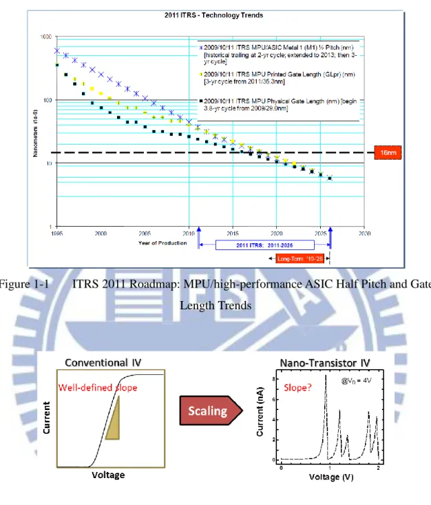
The first idea of the insulated-gate-field-effect transistor (IGFET) was invented by Lilienfeld [4] in his patent which can date back from 1926. However, the technology of these days was not mature enough to make sure the high-quality interface between the insulator and the semiconductor. In addition, the invention of bipolar transistor in 1947 [5] shifted most of research activities from IGFET to the potential-effect transistor (PET) [6]. This trend was changed since the metal-oxide-semiconductor filed-effect transistor (MOSFET) was firstly developed by Kahng and Atalla [7] in 1960. MOSFET has several advantages that hold well even in our day: 1) High speed switching, 2) Thermal stability (the current decrease with the temperature increase), and 3) Without offset voltage. After the invention of MOSFET by Kahng and Atalla [7], a rapid growth of the semiconductor industry started. The device dimension has been shrunk from the micrometer scale at its beginning to the present state-of-the-art, i.e., nano-meter scale. This is “BULK-to-NANO”. Figure 1-1 shows the forecast for transistor physical gate length during 2011-2026 from the International Technology Roadmap for Semiconductor (ITRS) 2011 [8]. It is aimed that the physical gate length will reach 16nm, 10nm, and 6nm in 2017, 2020, and 2026, respectively. Here note that 10nm is just fit to the de Broglie Length (DBL), which is a spatial width of electron wave in silicon materials. Nowadays, the semiconductor device design has become complicated by the demand of more functions to the integrated circuits and the progressive innovations in process engineering. The trial-and-error routine of the device design, which causes the significant reduction of cost-performance, has become out of date. On the other hand, it is hopefully expected that Technology Computer-Aided Design (TCAD) will compensate this reduction of the cost-performance. However, most of the TCAD tools, nowadays, still need many empirically-determined fitting parameters. The number of empirical parameters is also increased as the device scaling is advanced; which causes TCAD itself complicated. Until 2017 (16nm), the transport mechanism shall become away from the drift-diffusion model annually and, as a result, further more fitting parameters shall be required to fit the measured data. Until 2020 (10nm), the transport mechanism shall become much closer to full-quantum and far away from the drift-diffusion and it would be a challenge to fit the measured data. After 2020 (beyond 10nm), the transport mechanism in nano-devices shall be fully quantum-mechanical and then completely different from the drift-diffusion, as illustrated in
2
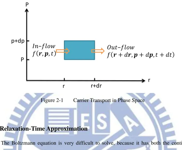
Figure 1-2. We can no more find a slope on the current-voltage characteristic of MOSFET, which is necessary to determine the mobility, in nano-device characteristics. We can no more fit the calculation results assuming the drift-diffusion with the measured data. How to design LSI? We are facing a historical turning point of the device engineering. Most of the important innovations in TCAD were made in the 1960s. Firstly, the exponential dependence was the major problem on numerical computing during 1960s [9]. Gummel proposed a decoupled iterative method in 1964, for solving the three coupled partial differential equations: Poisson equation, the electron continuity equation and the hole continuity equation [3]. In 1969, Scharfetter and Gummel presented a discretization method for the hole and electron current continuity equations, which can greatly reduce the computational resource for the device simulation [2]. Throughout ‘70s’ and ‘80s’, subsequently, most activities were devoted to the physical phenomena caused by device scaling [10], such as: the velocity overshoot effect [11], the hot-electron effect [12], and the narrow gate width effect [13]. These newly coming effects caused the researchers of the day to develop three-dimensional simulation [14] and Monte Carlo method [15].
The drift-diffusion (DD) model, which is adopted for the current equations of electron and hole has reproduced the measured device operation quite well so far. Nevertheless, we have to note the following matters: 1) DD model assumes the bulk body of semiconductor substrate. 2) We are reaching the period of nano-devices, as shown in Figure 1-1. Accordingly, whole new physical models must be implemented to a 3D general-purpose device simulator for nano-devices; meanwhile keeping the robustness and using less computational resources is also demanded.
3
Figure 1-1 ITRS 2011 Roadmap: MPU/high-performance ASIC Half Pitch and Gate Length Trends
4
Chapter 2.
Transport Theory
2.1 Boltzmann Transport Equation
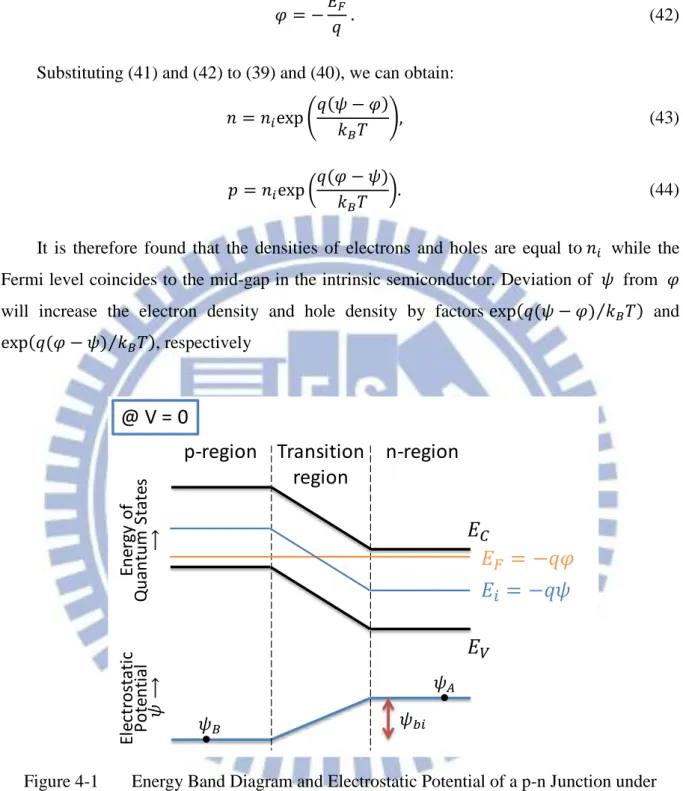
Let us regard carriers as classical particles; which dynamics are completely determined by assigning their positions 𝑟⃑ and momentums 𝑝⃑ at time t. Here, it is not necessary to consider about the size of carriers/particles. Next, let us consider a small region in the phase space about the point (𝑥, 𝑦, 𝑧, 𝑝𝑥, 𝑝𝑦, 𝑝𝑧), as shown in Figure 2-1, and the distribution function 𝑓(𝑟⃑, 𝑝⃑, 𝑡) which represents the probability to find a particle within this small region in phase space. The distribution function will change by 𝑓 during a time period 𝑡 as follows: 𝑓 = 𝑓(𝑥, 𝑦, 𝑧, 𝑝𝑥, 𝑝𝑦, 𝑝𝑧)
−𝑓(𝑥 + 𝑣𝑥 𝑡, 𝑦 + 𝑣𝑦 𝑡, 𝑧 + 𝑣𝑧 𝑡, 𝑝𝑥+𝐹𝑥 𝑡, 𝑝𝑦 + 𝐹𝑦 𝑡, 𝑝𝑧+ 𝐹𝑧 𝑡), (1) where 𝑣⃑ is the velocity of the considered carrier and 𝐹⃑ is the force field affecting on particle. Assuming the period 𝑡 is infinitesimally small and the distribution function is continuous in phase space, we can obtain:
𝑓
𝑡 + 𝑣⃑ ∙ ∇𝑟𝑓 + 𝐹⃑ ∙ ∇𝑝𝑓 = 0, (2) or using the 𝑘-representation:
𝑓
𝑡 + 𝑣⃑ ∙ ∇𝑟𝑓 + 𝐹⃑
ℏ∙ ∇𝑘𝑓 = 0. (3) Points in phase space express dynamical states. These points can enter into and be emitted out of a region while satisfying this equation just like a hydrodynamic flow. Generally speaking, we can involve scattering process into this equation. With the rate of change of distribution function due to scattering (𝜕𝑓𝜕𝑡)
𝑐𝑜𝑙𝑙, the distribution function turns out to be
satisfied to the equation: 𝑓 𝑡+ 𝑣⃑ ∙ ∇𝑟𝑓 + 𝐹⃑ ℏ∙ ∇𝑘𝑓 = ( 𝜕𝑓 𝜕𝑡)𝑐𝑜𝑙𝑙. (4) The right-hand side is called “collision-term”, which can break the continuity and cannot be defined uniquely. Here, it is noteworthy to say that the BTE is a strange equation. Firstly,
5
the left hand side should be continuous since it is written in terms of differentiation. Secondly, the right hand side can be discontinuous. In general, a discontinuous quantity cannot be equal to any continuous quantity. Accordingly, the treatment of the collision term has been a most sensitive issue in the history of modern physics. In terms of scattering theory, the contribution of scattering processes from a state 𝑘 to another state 𝑘 , and vice versa, to the collision term is written as:
𝑘 𝑘 𝑘 ( − 𝑘) − 𝑘 𝑘 𝑘( − 𝑓𝑘 ), (5)
where the 𝑘 𝑘, and 𝑘 𝑘 , represent the transition rates from 𝑘 to 𝑘 and from 𝑘 to 𝑘, respectively. Here 𝑘 depicts the occupation rate of state 𝑘. According to the Fermi’s Golden Rule [16], we can write:
𝑘 𝑘 =
2𝜋
ℏ |⟨𝑘|𝑉|𝑘 ⟩|2𝛿(𝐸𝑘− 𝐸𝑘 ), (6)
where V is the considered scattering potential, and 𝐸𝑘 and 𝐸𝑘 are the initial and final state energies of the particle that scatters.
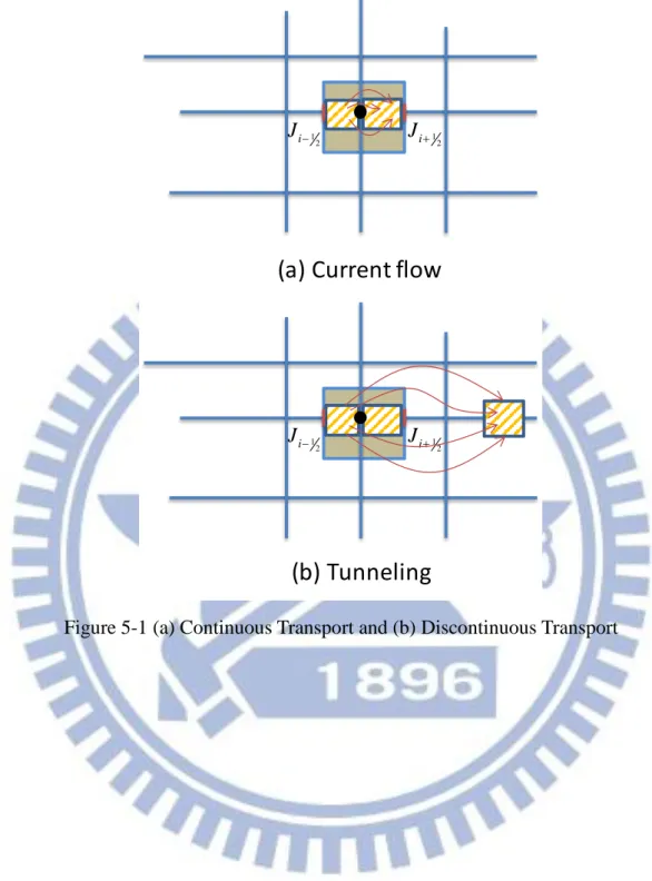
We must take into account more cases of contributions to the collision term. Most important in engineering is the process in which the number of particles is changed. For example, in electron tunneling phenomena, an electron disappears in anode where the tunneling starts, while an electron appears in cathode where the tunneling ends. The tunneling of electron decreases the number of electrons in anode and increase the number of electron in cathode. As long as we assume the energy band in semiconductor, the pair-creation and pair-annihilation of electron and hole can appear; which is called Shockley-Read-Hall (SRH) process. Since the creation of hole means the annihilation of valence electron, the total number of electrons in conduction band and valence band is unchanged. However, once we formulated the basic equations of electrons and holes separately, we must consider that the number of electrons (negative carriers; i.e., conduction electron) and the number of holes (positive carrier; a lack of valence electron) are increased at the same moment by SRH process. Moreover, we should note that the initial and end points of tunneling phenomena are regarded as spatially different, while no position change occurs in SRH process. Auger process can also increase the number of carriers.
6
𝑡 𝑓
𝑓 + , + , 𝑡 + 𝑡
𝑓
𝑓 , , 𝑡
P
r
r
r+dr
P
p+dp
Figure 2-1 Carrier Transport in Phase Space
2.2 Relaxation-Time Approximation
The Boltzmann equation is very difficult to solve, because it has both the continuous terms (related to the differential of the distribution function) and the discontinuous term (the collision term). In order to solve it, we have to make some simplification. Within the first order approximation, the most well-known is the relaxation-time approximation (RTA). In this approximation, we can replace the collision term with (𝑓0− 𝑓)/τ , where 𝑓0 is the distribution function at equilibrium condition and τ is the so-called relaxation time that specifies the time needed for the system to relax to its equilibrium state. Through a plenty of collisions, the distribution function shall be relaxed to the equilibrium state, i.e., equilibrated. In RTA, all the collisions are averaged and the essence of the collisions is involved to the relaxation time. We can no more discuss about each collision. In other words, the RTA gives us the view point of independent particle (with no collision). Here, we can distinguish three different types of relaxation times: 1) The collision time, which represents the average time to the next collision. This means that all primitive processes are averaged by the collision time, which is the same as the mean-free time in mean-field theory. The concept of this relaxation is valid with or without the conservation laws of energy and momentum. 2) The momentum relaxation time, which is the time needed for relaxing the momentum of a considered particle (individual from others within mean-field theory). Let us consider a particle with momentum higher than the average. The momentum of this particle is relaxed progressively with time.
7
This relaxation time is usually longer than the collision time, because it needs a plenty of collisions to relax the momentum of the considered particle. 3) The energy relaxation time, which is the time needed for relaxing the energy of considered particle. Let us consider a particle with energy higher than the average. The energy of this particle is relaxed progressively with time. This relaxation time is usually longer than the collision time, because it needs a plenty of collisions to relax the energy of considered particle. To consider all possibilities of the relaxations mentioned above from the view point of independent particle, we need to sum up all the inverse relaxation times to get the total relaxation time: ⁄ =𝜏𝑡 ∑ 𝜏𝑖 ⁄ k, where the subscript k represents the different relaxation view point, that is, k=1)
collision, k=2) momentum relaxation and k=3) energy relaxation.
To see more about the meaning of relaxation time, we assume a condition without external field and within a homogeneous semiconductor material. The BTE is reduced to:
∂𝑓 ∂𝑡 = −
𝑓 − 𝑓0
𝜏k , ℎ𝑒𝑟𝑒 ∇𝑟𝑓 = 0 𝑎 𝐹⃑ = 0. (7) Solving this differential equation with assuming the initial state of distribution function to be 𝑓𝑖, we can obtain:
𝑓 = 𝑓0+ (𝑓𝑖− 𝑓0)𝑒−𝑡 𝜏⁄ k. (8)
Here note that this result is valid for any k, i.e. the classification of relaxation. And we assume the relaxation time is independent of the velocity, position, and time.
8
Chapter 3.
Drift-Diffusion model
3.1 Drift-Diffusion Model Derivation
We can derive the drift-diffusion current equations from the BTE easily. The general expression of current equation is 𝐽⃑ = 𝑒 ∫ 𝑣⃑𝑓(𝑟⃑, 𝑣⃑, 𝑡) 3𝑣, where 𝑒 = −𝑞 for electrons and 𝑒 = 𝑞 for holes, and 𝑞 is the elementary charge. Firstly, let us consider a steady-state condition (𝜕𝑓𝜕𝑡 = 0 ), for simplicity, within 1D geometry. Using the relaxation-time approximation discussed above and the effective mass approximation (𝑝⃑ = 𝑚∗𝑣⃑), the BTE is
reduced to: 𝑣𝑥𝜕𝑓 𝜕𝑥+ 𝑒𝐸𝑥 𝑚∗ 𝜕𝑓 𝜕𝑣𝑥 = 𝑓0− 𝑓 𝜏 , (9)
where, 𝐸𝑥 is the electric field and we have used 𝐹𝑥 = 𝑒𝐸𝑥. Here note that the arguments of the distribution function are: the velocity, 𝑣⃑, and the location, 𝑥. The time, 𝑡, has been eliminated at steady state.
Thereby, we can obtain:
𝑓 = 𝑓0− [𝜏𝑣 𝑥 𝜕𝑓 𝜕𝑥+ 𝜏𝑒𝐸𝑥 𝑚∗ 𝜕𝑓 𝜕𝑣𝑥]. (10)
Substituting this into the current equation, we can obtain: 𝐽(𝑥) = 𝑒 ∫ 𝑣𝑥𝑓0 𝑣𝑥 +∞ −∞ − 𝑒 ∫ [𝜏𝑣𝑥2 𝜕𝑓 𝜕𝑥+ 𝑣𝑥𝜏𝑒𝐸𝑥 𝑚∗ 𝜕𝑓 𝜕𝑣𝑥] 𝑣𝑥 +∞ −∞ . (11) Since the equilibrium distribution function 𝑓0 is an even function, it is symmetrical in 𝑣⃑. The integral of the first term in the current equation must thereby be zero, that is, 𝑣𝑥𝑓0 is an odd function and then the integration must be zero over an even integration interval. Since the relaxation time is assumed to be independent of 𝑣⃑, we have the following expression:
𝐽(𝑥) = −𝑒 ∫ 𝜏𝑣𝑥2𝜕𝑓(𝑣𝑥, 𝑥) 𝜕𝑥 𝑣𝑥 +∞ −∞ − 𝑒 ∫ 𝑣𝑥𝜏𝑒𝐸𝑥 𝑚∗ 𝜕𝑓(𝑣𝑥, 𝑥) 𝜕𝑣𝑥 𝑣𝑥 +∞ −∞ = −𝑒𝜏 𝜕 𝜕𝑥∫ 𝑣𝑥2𝑓(𝑣𝑥, 𝑥) 𝑣𝑥 +∞ −∞ −𝑒 2𝜏𝐸 𝑥 𝑚∗ ∫ 𝑣𝑥 𝑓(𝑣𝑥, 𝑥) +∞ −∞ . (12) The first term in the right hand side is rewritten as:
9
∫ 𝑣𝑥2𝑓(𝑣𝑥, 𝑥) 𝑣𝑥 +∞
−∞
〈𝑣𝑥2〉𝑐(𝑥), (13)
where 〈𝑣𝑥2〉 is the average of the square of the velocity and 𝑐(𝑥) stands for the carrier
concentration, 𝑐(𝑥) = ∫−∞+∞𝑓(𝑣𝑥, 𝑥) 𝑣𝑥. According to the energy equipartition rule:
𝑚∗
2〈𝑣𝑥2〉 = 1
2𝑘𝐵𝑇 with 𝑇 being the absolute temperature, the first term turns out to be:
−𝑒𝜏 𝜕 𝜕𝑥{〈𝑣𝑥2〉𝑐(𝑥)} = −𝑒𝜏〈𝑣𝑥2〉 𝜕 𝜕𝑥{𝑐(𝑥)} = −𝑒𝜏 𝑚∗𝑘𝐵𝑇 𝜕𝑐(𝑥) 𝜕𝑥 = −𝑒 𝑞𝜇𝑘𝐵𝑇 𝜕𝑐(𝑥) 𝜕𝑥 = −𝑒𝐷 𝑥𝑐(𝑥). (14)
Here we assume: 𝜇 = 𝑞𝜏 𝑚⁄ ∗, i.e. the mobility, and the Einstein relation, 𝐷 𝜇⁄ =
𝑘𝐵𝑇 𝑞⁄ , where 𝑒 = −𝑞 for electrons and 𝑒 = 𝑞 for holes. It should be noted that T concerns
the temperature of electron-hole gases in DD model with regardless of any lattice motion. This means DD model itself cannot involve any phonon process. For the second term of the right hand side, by using integration by parts, we can obtain:
−𝑞2𝜏𝐸𝑥 𝑚∗ ∫ 𝑣𝑥 𝑓(𝑣𝑥, 𝑥) +∞ −∞ = −𝑞2𝜏𝐸𝑥 𝑚∗ [𝑣𝑥𝑓|−∞+∞− ∫ 𝑓 𝑣𝑥 +∞ −∞ ], (15) where 𝑒2 = 𝑞2. Assuming 𝑓(+∞, 𝑥) = 𝑓(−∞, 𝑥) = 0 and ∫−∞+∞𝑓 𝑣𝑥 = 𝑐(𝑥), the second
term turns out to be: −𝑒 2𝜏𝐸 𝑥 𝑚∗ ∫ 𝑣𝑥 𝑓(𝑣𝑥, 𝑥) +∞ −∞ 𝑞𝜇𝐸𝑥𝑐(𝑥). (16)
Finally, we have the current density equation: 𝐽(𝑥) = 𝑞𝜇𝐸𝑥𝑐(𝑥) − 𝑒𝐷
𝑥𝑐(𝑥). (17)
Substituting 𝑒 = −𝑞 , 𝜇 = 𝜇𝑛, and 𝐷 = 𝐷𝑛for electrons and 𝑒 = 𝑞 , 𝜇 = 𝜇𝑝, and 𝐷 = 𝐷𝑝 for holes, we can obtain the drift-diffusion equations for electrons and holes
𝐽𝑛(𝑥) = 𝑞 (𝑥)𝜇𝑛𝐸𝑥+ 𝑞𝐷𝑛
𝜕 (𝑥)
10
𝐽𝑝(𝑥) = 𝑞𝑝(𝑥)𝜇𝑝𝐸𝑥− 𝑞𝐷𝑝
𝜕𝑝(𝑥)
𝜕𝑥 . (19)
3.2 Continuity Equation
Using the law of particle conservation, we derive the continuity equation from BTE: 𝑓(𝑟⃑, 𝑘⃑⃑, 𝑡) 𝑡 + 𝑣⃑ ∙ ∇𝑟𝑓(𝑟⃑, 𝑘⃑⃑, 𝑡) + 𝐹⃑ ℏ∙ ∇𝑘𝑓(𝑟⃑, 𝑘⃑⃑, 𝑡) = ( 𝜕𝑓(𝑟⃑, 𝑘⃑⃑, 𝑡) 𝜕𝑡 ) 𝑐𝑜𝑙𝑙 . (20) Integrating (20) over all k space, we then obtain:
∭𝜕𝑓 𝜕𝑡 𝑘⃑⃑ + ∭ 𝑣⃑ ∙ ∇𝑟𝑓 𝑘⃑⃑ + ∭ 𝐹⃑ ℏ∙ ∇𝑘𝑓 𝑘⃑⃑ = ∭ ( 𝜕𝑓 𝜕𝑡)𝑐𝑜𝑙𝑙 𝑘⃑⃑. (21) The second term in the left hand side of (21) is reduced to:
∭ 𝑣⃑ ∙ ∇𝑟𝑓 𝑘⃑⃑ = ∭ ∇𝑟∙ (𝑣⃑𝑓) 𝑘⃑⃑ − ∭ 𝑓∇𝑟∙ 𝑣⃑ 𝑘⃑⃑. (22) Since 𝑣⃑ is explicitly independent of 𝑟⃑, this term ∇𝑟∙ 𝑣⃑ will be zero; which results in:
∭ 𝑣⃑ ∙ ∇𝑟𝑓 𝑘⃑⃑ = ∇𝑟∙ ∭ 𝑣⃑𝑓(𝑟⃑, 𝑘⃑⃑, 𝑡) 𝑘⃑⃑ = ∇𝑟∙ (
𝑒𝐽⃑), (23) where 𝐽⃑ is an electric current. Assuming that the distribution function 𝑓 is zero while the wavenumber is very high, the third term in the left hand side of (21) turns out to be:
∭𝐹⃑ ℏ∙ ∇𝑘𝑓 𝑘⃑⃑ =ℏ∭(𝐹𝑥, 𝐹𝑦, 𝐹𝑧) ∙ ( 𝜕𝑓 𝜕𝑘𝑥, 𝜕𝑓 𝜕𝑘𝑦, 𝜕𝑓 𝜕𝑘𝑥) 𝑘⃑⃑ = ℏ∭ (𝐹𝑥 𝜕𝑓 𝜕𝑘𝑥+ 𝐹𝑦 𝜕𝑓 𝜕𝑘𝑦+ 𝐹𝑧 𝜕𝑓 𝜕𝑘𝑥) 𝑘𝑥 𝑘𝑦 𝑘𝑧= 0. (24) Here we also have used the integration by parts, in the similar manner to (15) and note that the force is independent of the momentum. The integration of the collision term, i.e., the right hand side of (21), can be a-priori replaced by the generation-recombination term as follows:
∭ (𝜕𝑓
𝜕𝑡)𝑐𝑜𝑙𝑙 𝑘⃑⃑ = 𝐺 − 𝑅. (25)
11
𝜕
𝜕𝑡𝑐(𝑟⃑, 𝑡) +𝑒∇𝑟∙ 𝐽⃑ = 𝐺 − 𝑅, (26) where we have adopted:
∭ 𝑓 𝑘⃑⃑ ≡ 𝑐(𝑟⃑, 𝑡). (27) Regarding that 𝑐(𝑥) = (𝑥), which is the electron density, for electrons, and 𝑐(𝑥) = 𝑝(𝑥), which is the hole density, for holes, and note that 𝑒 = −𝑞 for electrons and 𝑒 = 𝑞 for holes. From (26), we can have the current continuity equation for electrons and holes as follows:
𝜕
𝜕𝑡 −𝑞∇𝑟∙ 𝐽⃑𝑛 = 𝐺𝑛− 𝑅𝑛, (28) 𝜕𝑝
𝜕𝑡 +𝑞∇𝑟∙ 𝐽⃑𝑝 = 𝐺𝑝− 𝑅𝑝, (29) Where 𝐺𝑛 and 𝐺𝑝 are the generation rates of electrons and holes, respectively, and 𝑅𝑛 and 𝑅𝑝 are the recombination rates of electrons and holes, respectively. 𝐽⃑𝑛 and 𝐽⃑𝑝 are the electric currents of electrons and holes, respectively, which are described by the drift-diffusion model.
As mentioned above, we replaced the collision term with the relaxation term, (𝑓0− 𝑓) 𝜏⁄ ,
within the first order approximation, i.e., RTA. Subsequently, we appended the generation-recombination terms as a correction to the relaxation term by hand. This correction is no more than a part of the second and higher order terms of the collision term, but it was carefully deduced to catch the physical intuition related to some deviations from the drift-diffusion model. However, as the device scaling is progressed, we shall be forced to involve more correction terms that may be discontinuous. The discontinuity is enhanced with the scaling, and then, once entering the period of nano-devices, the discontinuous terms must prevail over the continuous term. As long as the drift-diffusion model is adopted, we cannot find any solution in nano-devices.
3.3 Poisson Equation
12
∇ ∙ (𝜖𝐸⃑⃑) = 𝜌, (30)
where 𝜌 is the charge density and 𝜖 is the permittivity. With the definition of the electric field (𝐸⃑⃑):
𝐸⃑⃑ = −∇𝜓, (31)
here 𝜓 represents the static potential, we can combine these two equations and assuming ϵ is a constant to obtain
∇ ∙ ∇𝜓 = −𝜌
𝜖. (32)
In a semiconductor material, we can express the charge density as 𝜌 = 𝑞(𝑝 − + 𝑁𝐷+ − 𝑁
𝐴−), (33)
where 𝑁𝐷+ is the ionized donor concentration and 𝑁𝐴− is the ionized acceptor concentration. By the above equations, the Poisson equation in a homogeneous semiconductor is given by, ∇2𝜓 = −𝑞 𝜖(𝑝 − + 𝑁𝐷+− 𝑁𝐴−). (34) In Cartesian form, ∂2𝜓 ∂x2 + ∂2𝜓 ∂y2 + ∂2𝜓 ∂z2 = − 𝑞 𝜖(𝑝 − + 𝑁𝐷+− 𝑁𝐴−). (35)
13
Chapter 4.
Numerical Solutions
4.1 Concept of Quasi-Equilibrium
The Poisson equation, the continuity equations for electrons and holes with the drift-diffusion models are simultaneous equations that have three variables, 𝜓, , and 𝑝.
∇2𝜓 = −𝑞
𝜖(𝑝 − + 𝑁𝐷+− 𝑁𝐴−). (36) ∇ ∙ ( 𝜇𝑛∇𝜓 − 𝐷𝑛∇ ) = 𝐺𝑛− 𝑅𝑛. (37) ∇ ∙ (−𝑝𝜇𝑝∇𝜓 − 𝐷𝑝∇𝑝) = 𝐺𝑝− 𝑅𝑝. (38) However, there are some numerical issues about using this set of variables, (𝜓, , 𝑝), to simulate semiconductor devices. One of them is the exponential dependency of carrier concentrations, and 𝑝, on the electrostatic potential, 𝜓; which increases the risk of numerical errors in calculation results.
In terms of mass-action law, we can write the relation between the carrier concentrations and the Fermi level, 𝐸𝐹 as below:
= 𝑖exp (𝐸𝐹 − 𝐸𝑖
𝑘𝐵𝑇 ), (39)
𝑝 = 𝑖exp (
𝐸𝑖 − 𝐸𝐹
𝑘𝐵𝑇 ), (40)
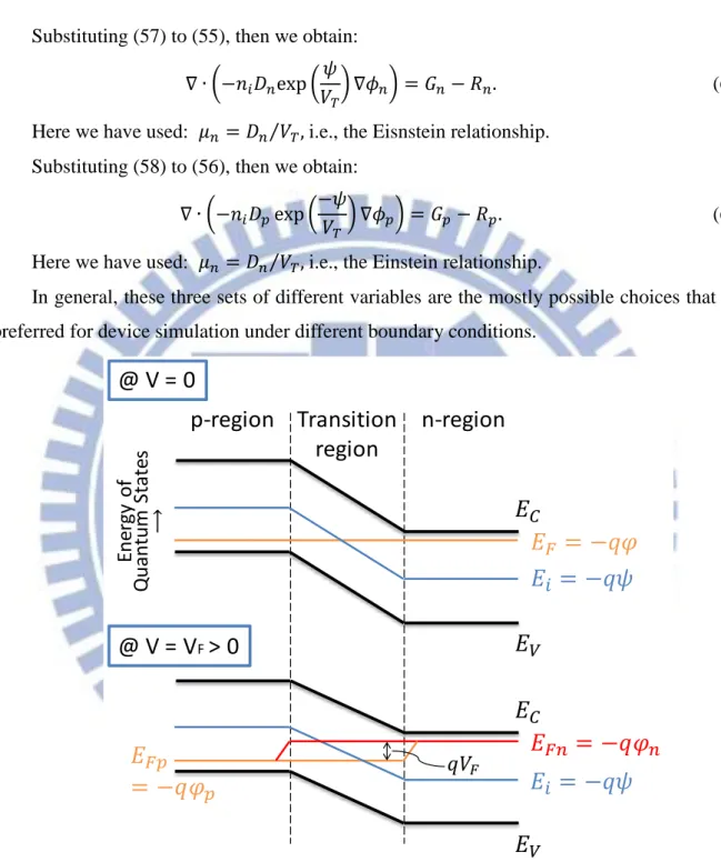
where 𝑖 is the intrinsic density and 𝐸𝑖 is the mid-gap energy [17]. Let us assume that the origin of the potential is the mid-gap energy in the p-type region across the p-n junction shown in Figure 4-1 and then we can write:
𝐸𝑖 = −𝑞𝜓. (41)
As shown in the upper illustration in Figure 4-1, 𝐸𝑖 is decreased by the build-in-potential multiplied by 𝑞 across the p-n junction at equilibrium (with no bias). At the same moment, 𝜓 is increased by the build-in-potential across the p-n junction, as shown in the bottom illustration. Next, let us introduce the Fermi level1 as follows:
1 Let us call both 𝐸
14
𝜑 = −𝐸𝐹
𝑞 . (42)
Substituting (41) and (42) to (39) and (40), we can obtain: = 𝑖exp ( 𝑞(𝜓 − 𝜑) 𝑘𝐵𝑇 ), (43) 𝑝 = 𝑖exp ( 𝑞(𝜑 − 𝜓) 𝑘𝐵𝑇 ). (44)
It is therefore found that the densities of electrons and holes are equal to 𝑖 while the
Fermi level coincides to the mid-gap in the intrinsic semiconductor. Deviation of 𝜓 from 𝜑 will increase the electron density and hole density by factors exp(𝑞(𝜓 − 𝜑) 𝑘⁄ 𝐵𝑇) and exp(𝑞(𝜑 − 𝜓) 𝑘⁄ 𝐵𝑇), respectively
𝐸
𝐸
𝐸
𝑖= −𝑞𝜓
𝐸
𝐹= −𝑞𝜑
p-region
Transition
n-region
region
El ec tr o sta ti c P ot enti al Ene rg y o f Q uant um S ta te s 𝜓𝐵 𝜓𝐴 𝜓 𝑖@ V = 0
Figure 4-1 Energy Band Diagram and Electrostatic Potential of a p-n Junction under Equilibrium
When a forward voltage (𝑉𝐹) is applied to a p-n junction, as shown in Figure 4-2, the
equilibrium condition is broken and then the electron-hole system will seek for a secondary statistical balance, which is called the quasi-equilibrium state. In this event, we may define the quasi-Fermi level separately for the electron density and the hole density as follows:
𝐸
𝐶𝐸
𝑉𝐸
𝑖= −𝑞𝜓
𝐸
𝐹= −𝑞𝜑
p-region
Transition
n-region
region
⟶
Ener
gy
of
Q
ua
n
tum St
at
es
𝜓
𝐴15 ≡ 𝑖exp (𝐸𝐹𝑛 − 𝐸𝑖 𝑘𝐵𝑇 ), (45) 𝑝 ≡ 𝑖exp (𝐸𝑖 − 𝐸𝐹𝑝 𝑘𝐵𝑇 ), (46) 𝑟 ≡ 𝑖exp (𝑞(𝜓 − 𝜑𝑛) 𝑘𝐵𝑇 ), (47) 𝑝 ≡ 𝑖exp (𝑞(𝜑𝑝− 𝜓) 𝑘𝐵𝑇 ), (48)
where 𝐸𝐹𝑛 = −𝑞𝜑𝑛 and 𝐸𝐹𝑝 = −𝑞𝜑𝑝 are the quasi-Fermi levels for electrons2 and holes3, respectively.
From the above equations, we can derive the quasi-Fermi levels for electrons and holes as follows: 𝜑𝑛 ≡ 𝜓 −𝑘𝐵𝑇 𝑞 ln ( 𝑖), (49) 𝜑𝑝 ≡ 𝜓 +𝑘𝐵𝑇 𝑞 ln ( 𝑝 𝑖), (50)
respectively. Figure 4-2 illustrates the 𝐸𝐹𝑛 and 𝐸𝐹𝑝 throughout the p-n junction under quasi-equilibrium condition with forward bias, 𝑉𝐹. It is noteworthy that the Fermi level 𝐸𝐹
is defined under equilibrium condition, while 𝐸𝐹𝑛− 𝐸𝐹𝑝 = 𝑞𝑉𝐹 under quasi-equilibrium condition with 𝑉𝐹.
Using 𝜑𝑛, 𝜑𝑝, eq. (47), and the Einstein relationship, the current density equation for electron turns out to be:
2 Let us call both 𝐸
𝐹𝑛 and 𝜑𝑛 “Fermi level” in this thesis.
3
16 𝐽⃑𝑛 = 𝑞 𝜇𝑛𝐸⃑⃑ + 𝑞𝐷𝑛∇ = −𝑞 𝜇𝑛∇𝜓 + 𝑞𝐷𝑛∇ ( 𝑖exp (𝑞(𝜓 − 𝜑𝑛) 𝑘𝐵𝑇 )) = −𝑞 𝜇𝑛∇𝜓 + 𝑞𝐷𝑛 𝑖 𝑞 𝑘𝐵𝑇exp ( 𝑞(𝜓 − 𝜑𝑛) 𝑘𝐵𝑇 ) ∇(𝜓 − 𝜑𝑛) = −𝑞 𝜇𝑛∇𝜓 + 𝑞𝜇𝑛 ∇(𝜓 − 𝜑𝑛) = −𝑞𝜇𝑛 ∇𝜑𝑛. (51)
In similar way, we can derive:
𝐽⃑𝑝 = −𝑞𝜇𝑝𝑝∇𝜑𝑝. (52)
The equations (51) and (52) are quite similar to the current density in conductor:
𝐽⃑ = −𝑞𝜇 ∇𝜓. (53)
Now we can use the electron and hole quasi-Fermi levels to define a new set of the equations. Here, 𝜓 is the electrostatic potential that can be defined at any location of considered semiconductor material. Substituting (47) and (48) to (36), we can obtain:
∇2𝜓 = −𝑞 𝑖 𝜖 (exp ( 𝜑𝑝− 𝜓 𝑉𝑇 ) − exp ( 𝜓 − 𝜑𝑛 𝑉𝑇 ) + 𝑁𝐷 +− 𝑁 𝐴−). (54)
here 𝑉𝑇 = 𝑘𝐵𝑇 𝑞⁄ represents the thermal voltage.
Substituting (47) to (37), we can obtain: ∇ ∙ (𝜇𝑛 𝑖exp (𝜓 − 𝜑𝑛
𝑉𝑇 ) ∇𝜑𝑛) = 𝐺𝑛 − 𝑅𝑛. (55)
Substituting (48) to (38), we can obtain: ∇ ∙ (−𝜇𝑝 𝑖exp (
𝜑𝑝− 𝜓
𝑉𝑇 ) ∇𝜑𝑝) = 𝐺𝑝− 𝑅𝑝. (56)
Furthermore, we can change the choice of variables according to Slotboom [18] as follows: 𝜙𝑛 = exp ( −𝜑𝑛 𝑉𝑇 ), (57) 𝜙𝑝 = exp ( 𝜑𝑝 𝑉𝑇). (58)
17 ∇2𝜓 = −𝑞 𝑖 𝜖 (𝜙𝑝exp ( −𝜓 𝑉𝑇) − 𝜙𝑛exp ( 𝜓 𝑉𝑇) + 𝑁𝐷 +− 𝑁 𝐴−). (59)
Substituting (57) to (55), then we obtain: ∇ ∙ (− 𝑖𝐷𝑛exp (𝜓
𝑉𝑇) ∇𝜙𝑛) = 𝐺𝑛− 𝑅𝑛. (60) Here we have used: 𝜇𝑛 = 𝐷𝑛⁄ , i.e., the Eisnstein relationship. 𝑉𝑇
Substituting (58) to (56), then we obtain: ∇ ∙ (− 𝑖𝐷𝑝exp (
−𝜓
𝑉𝑇) ∇𝜙𝑝) = 𝐺𝑝− 𝑅𝑝. (61) Here we have used: 𝜇𝑛 = 𝐷𝑛⁄ , i.e., the Einstein relationship. 𝑉𝑇
In general, these three sets of different variables are the mostly possible choices that are preferred for device simulation under different boundary conditions.
𝐸
𝐸
p-region
Transition
n-region
region
Ene rg y o f Q uant um S tat es𝐸
𝐸
𝐸
𝐹𝑝= −𝑞𝜑
𝑝𝐸
𝐹𝑛= −𝑞𝜑
𝑛𝐸
𝑖= −𝑞𝜓
𝐸
𝑖= −𝑞𝜓
𝐸
𝐹= −𝑞𝜑
@ V = V
F> 0
@ V = 0
𝑞𝑉𝐹Figure 4-2 Energy Band Diagram under Equilibrium and Forward Biased
4.2 Discretization of the Poisson Equation
We can discretize the Poisson equation using a finite-difference scheme [19]. Considering Taylor’s expansion in a case of one-dimension (1D),
18 𝑓(𝑥𝑖 + ∆𝑥) = 𝑓(𝑥𝑖) + 𝑓 (𝑥𝑖)(∆𝑥) +𝑓 (𝑥𝑖) 2 (∆𝑥)2+ ⋯, (62) 𝑓(𝑥𝑖 − ∆𝑥) = 𝑓(𝑥𝑖) − 𝑓 (𝑥𝑖)(∆𝑥) − 𝑓 (𝑥 𝑖) 2 (∆𝑥)2− ⋯, (63) where 𝑓 (𝑥𝑖) and 𝑓 (𝑥𝑖) represent the first and second derivative of the function 𝑓(𝑥) at point 𝑥𝑖, respectively. Subtracting (62) from (63) and ignoring the high order terms, we can approximate the first and second derivatives as
𝑓 (𝑥𝑖) ≅ 𝑓(𝑥𝑖+ ∆𝑥) − 𝑓(𝑥𝑖 − ∆𝑥) 2(∆𝑥) , (64) 𝑓 (𝑥 𝑖) ≅ 𝑓(𝑥𝑖 + ∆𝑥) + 𝑓(𝑥𝑖 − ∆𝑥) − 2𝑓(𝑥𝑖) (∆𝑥)2 , (65)
respectively. If a nonuniform rectangular mesh is adopted, i.e. ℎ𝑖+1 ≠ ℎ𝑖, as depicted in Figure 4-3, the approximations become
𝑓 (𝑥𝑖) ≅ 𝑓(𝑥𝑖+1) − 𝑓(𝑥𝑖−1) ℎ𝑖+1+ ℎ𝑖 , (66) 𝑓 (𝑥 𝑖) ≅ 2 ℎ𝑖+1+ ℎ𝑖[ 𝑓(𝑥𝑖+1) − 𝑓(𝑥𝑖) ℎ𝑖+1 + 𝑓(𝑥𝑖−1) − 𝑓(𝑥𝑖) ℎ𝑖 ], (67) where ℎ𝑖 ≡ 𝑥𝑖 − 𝑥𝑖−1.
With the finite-difference discretization [19] in a case of three-dimension (3D), we can approximate the left hand side of (59) at a mesh point (𝑖, 𝑗, ) as follows:
𝜕2𝜓 𝜕𝑥2| 𝑖,𝑗,𝑙 ≅ 2 ℎ𝑖+1+ ℎ𝑖[ 𝜓𝑖+1,𝑗,𝑙− 𝜓𝑖,𝑗,𝑙 ℎ𝑖+1 + 𝜓𝑖−1,𝑗,𝑙− 𝜓𝑖,𝑗,𝑙 ℎ𝑖 ], (68) 𝜕2𝜓 𝜕𝑦2| 𝑖,𝑗,𝑙 ≅ 2 𝑘𝑗+1+ 𝑘𝑗[ 𝜓𝑖,𝑗+1,𝑙− 𝜓𝑖,𝑗,𝑙 𝑘𝑗+1 + 𝜓𝑖,𝑗−1,𝑙− 𝜓𝑖,𝑗,𝑙 𝑘𝑗 ], (69) 𝜕2𝜓 𝜕𝑧2| 𝑖,𝑗,𝑙 ≅ 2 𝑙+1+ 𝑙[ 𝜓𝑖,𝑗,𝑙+1− 𝜓𝑖,𝑗,𝑙 𝑙+1 + 𝜓𝑖,𝑗,𝑙−1− 𝜓𝑖,𝑗,𝑙 𝑙 ], (70) where 𝑘𝑗 ≡ 𝑦𝑗− 𝑦𝑗−1 and 𝑙≡ 𝑧𝑙− 𝑧𝑙−1.
19 2 ℎ𝑖+1+ ℎ𝑖[ 𝜓𝑖+1,𝑗,𝑙− 𝜓𝑖,𝑗,𝑙 ℎ𝑖+1 + 𝜓𝑖−1,𝑗,𝑙− 𝜓𝑖,𝑗,𝑙 ℎ𝑖 ] + 2 𝑘𝑗+1+ 𝑘𝑗[ 𝜓𝑖,𝑗+1,𝑙− 𝜓𝑖,𝑗,𝑙 𝑘𝑗+1 + 𝜓𝑖,𝑗−1,𝑙− 𝜓𝑖,𝑗,𝑙 𝑘𝑗 ] + 2 𝑙+1 + 𝑙[ 𝜓𝑖,𝑗,𝑙+1− 𝜓𝑖,𝑗,𝑙 𝑙+1 + 𝜓𝑖,𝑗,𝑙−1− 𝜓𝑖,𝑗,𝑙 𝑙 ] = −𝑞 𝑖 𝜖 (𝜙𝑝(𝑖,𝑗,𝑙)exp ( −𝜓𝑖,𝑗,𝑙 𝑉𝑇 ) − 𝜙𝑛(𝑖,𝑗,𝑙)exp ( 𝜓𝑖,𝑗,𝑙 𝑉𝑇 ) + 𝑁𝐷(𝑖,𝑗,𝑙)+ − 𝑁𝐴(𝑖,𝑗,𝑙)− ). (71) In the above, we have assumed the permittivity is constant to discretize the Poisson equation. However, the permittivity is varying over several angstroms and more (around one nanometer) [22]. The constant permittivity assumption is invalid in General-Purpose Nano Device simulation. To follow up the permittivity change inside nano-devices, it is preferable to replace the left-hand side of (71) with the discretized surface integral of continuous flux under the finite-difference scheme [19].
X
X
iX
i+1X
i-1h
ih
i+1f(X)
Approximated
f’(X
i)
Exact
f’(X
i)
Figure 4-3 Graphical Illustration of Finite Difference Discretization
4.3 Control Volume
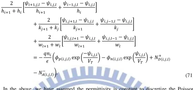
Generally, the continuous space coordinate can be discretized using the finite-difference scheme [19], in which discretization cell is called “control volume”. Continuous matters can also be divided according to the set of control volumes. We must then carefully consider how the continuity of matters can be confirmed at each control volume.
20
Hydrodynamics simulation has been extensively adopted to study the dynamics of continuous matters. In semiconductor device physics, the drift-diffusion model is adopted to describe the continuity of the carrier transport. Moreover, the generation-recombination term is added, and can then break the continuity. Nevertheless, assuming that the elementary charge (causing the discontinuity) is too small to be detected in the carrier transport phenomena; we have treated the device simulation using hydrodynamic formulation with the control volume. Here note that the drift-diffusion model is confined within the divergence of the continuity equation, as shown in (55) and (56). Let us consider the numerical fluxes that will inject to and ejected from a control volume, in which the divergence theorem is satisfied as follows:
∬ ∇ ∙ 𝐹⃑ 𝐴𝑠 = ∮ 𝐹⃑ ∙ ⃑⃑ 𝑠𝜕𝑠 , (72) where 𝑠 represents the control volume, ∂𝑠 represents the boundary of the control volume, as illustrated in Figure 4-4, 𝐴 represents the volume element of the control volume, 𝐹⃑ is the flux vector related to the control volume, and 𝑠 represents the surface element on the boundary of the control volume. We can thereby replace the divergence of the vector function with the surface integral on the boundary of the control volume. This is the key to discretize Poisson equation and the continuity equations for electrons and holes [20].
We have three independent variables in the formulation, for example, potential, electron density, and hole density. First of all, these independent variables are put on each mesh point. The first‐ order differentiations of these variables are defined as the increment between adjoining mesh points; which may put on the middle point between these adjoining mesh points. It is noteworthy to say that these middle points are on the boundary of the control volume. Thereby, we can illustrate the control volume, as shown in Figure 4-4. Independent variables are put on mesh points, while the first differentiations of these variables are put on the boundary of the control volume that bounds the mesh point. The aforementioned surface integral is carried out on this boundary. The second differentiations are, on the other hand, defined as the increments between the midpoints on the boundary of the control volume. As a result, the second differentiations are put on mesh points that are centered in control volumes. If 𝐹 ⃑⃑⃑⃑ is electric current, it is a first differentiation of carrier densities that are independent variables. If 𝐹 ⃑⃑⃑⃑ is electric field, it is a first differentiation of potential that is an independent variable. The divergences of the electron current, hole current and electric field are therefore put on mesh points and are replaced by the surface integration around the boundary of the
21
control volume with continuous flux (𝐹 ⃑⃑⃑⃑). Poisson equation is, on the other hand, written in the second differentiation of potential (put on mesh point in control volume). The continuity equations are written in the second differentiation of carrier densities (put on mesh point in control volume). Therefore, the basic formulation of the device physics is written on mesh points (in control volume), while we use control volumes to perform the device simulation. As long as continuous matters satisfy the divergence theorem (72), we can thereby discretize the equations of the continuous matters on the boundary of control volume. As long as the
electric field and the electric current are regarded as (continuous) fluxes, the finite volume method with control volume is valid to the device physics. For the simplicity, let us assume
that the permittivity is distributed in the control volume on the two-dimensional rectangular mesh, as shown in Figure 4-4(b). Using (72), the integration of (71) results in:
(𝜖1 𝑖+1+ 𝜖8 𝑖)(𝜓𝑖,𝑗+1− 𝜓𝑖,𝑗) 2𝑣𝑖 + (𝜖7𝑣𝑖 + 𝜖6𝑣𝑖+1) (𝜓𝑖−1,𝑗− 𝜓𝑖,𝑗) 2 𝑖 + (𝜖4 𝑖+1+ 𝜖5 𝑖)(𝜓𝑖,𝑗−1− 𝜓𝑖,𝑗) 2𝑣𝑖 + (𝜖3𝑣𝑖+1+ 𝜖2𝑣𝑖) (𝜓𝑖+1,𝑗− 𝜓𝑖,𝑗) 2 𝑖+1 = −𝑞 𝑖(𝜙𝑝(𝑖,𝑗)exp ( −𝜓𝑖,𝑗 𝑉𝑇 ) − 𝜙𝑛(𝑖,𝑗)exp ( 𝜓𝑖,𝑗 𝑉𝑇) + 𝑁𝐷(𝑖,𝑗) + − 𝑁𝐴(𝑖,𝑗)− )(ℎ𝑖+1+ℎ𝑖)(𝑘𝑗+1+𝑘𝑗) 4 . (73)
It should be noted that the control volume is consistent to the meshing by the finite difference scheme [19].
Figure 4-4 The Control Volume 𝑠 and Boundary ∂𝑠 Defined by Perpendicular Bisectors of Mesh Grid in (a) Triangular Mesh and (b) Rectangular Mesh.
22
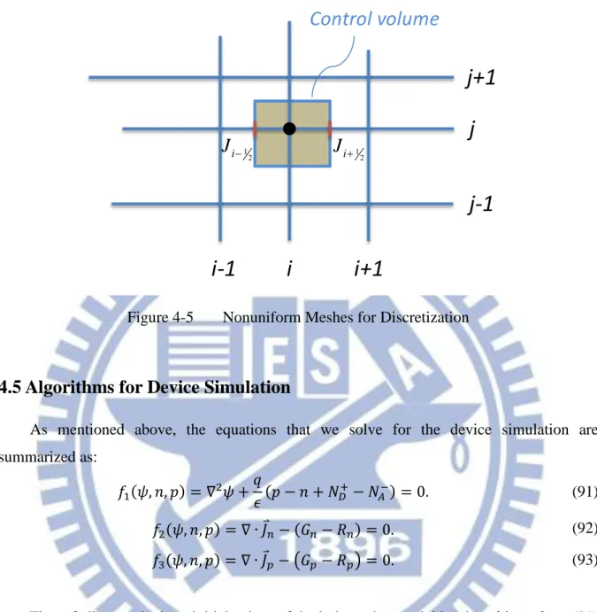
4.4 Scharfetter-Gummel Discretization for Continuity Equations
For the hole and electron current continuity equations, we can discretize them, similar to the above, i.e., by the finite-difference approach [19]. It is implicitly assumed that the same control volume is adopted as the discretization of Poisson equation. From Figure 4-5, we can approximate the electron current continuity equation (28) in 𝑥 direction as:
𝑖
𝑡 ≅ 𝐺𝑛(𝑖)− 𝑅𝑛(𝑖)+𝑞 𝐽⃑𝑖+1
2− 𝐽⃑𝑖−12
∆𝑥 . (74)
Next issue is the meshing in real space. Here note that any linearly-gradual meshing gives rise to a significant problem, which is numerical instability owing to the exponential change of the carrier density to the potential. We can see this exponential dependence considering a 1D case of equation (60),
𝑥(− 𝑖𝐷𝑛exp ( 𝜓 𝑉𝑇) 𝜙𝑛 𝑥 ) = 𝐺𝑛− 𝑅𝑛. (75) We can express it as 2𝜙 𝑛 𝑥2 +𝑉 𝑇 𝜓 𝑥 𝜙𝑛 𝑥 = − 𝐺𝑛 − 𝑅𝑛 𝑖𝐷𝑛𝑒 𝜓 𝑉𝑇 . (76)
Assuming the electric field, 𝐸𝑥 = −𝑑𝜓𝑑𝑥 as a constant for simplicity, the solution of this ordinary differential equation satisfies the following form:
𝜙𝑛 = 𝐶1+ 𝐶2𝑒𝐸𝑥𝑉𝑇+ 𝑔(𝑥), (77) where 𝑔(𝑥) represents the particular solution and 𝐶1 and 𝐶2 are arbitrary numbers. It is obvious that 𝜙𝑛 is mainly an exponential function of the electric field.
In order to overcome this problem, Scharfetter and Gummel pointed out that the potential varies linearly across mesh points, while the carrier density varies exponentially. The carrier density equations are regarded as differential equations, in which 𝐽⃑𝑛, 𝐽⃑𝑝, 𝜇𝑛, 𝜇𝑝, and 𝐸⃑⃑ are assumed constants between mesh points. In a case of 1D, we can thereby write the electron current density as follows:
𝐽𝑛𝑥 = 𝑞𝐷𝑛 𝑖𝑒
𝜓 𝑉𝑇 𝜙𝑛
𝑥 = 𝑐 𝑠𝑡., 𝑥𝑖 < 𝑥 < 𝑥𝑖+1. (78) It can be written as
23 𝜙𝑛 = 𝑞𝐷𝐽𝑛𝑥 𝑛𝑛𝑖𝑒 −𝜓 𝑉𝑇 𝑥, 𝑥𝑖 < 𝑥 < 𝑥𝑖+1. (79) Substituting 𝑒− 𝜓 𝑉𝑇 𝑥 = −𝑑𝜓𝑇 𝑑𝑥
(𝑒−𝑉𝑇𝜓) into the above equation, then we obtain
𝜙𝑛 = − 𝐽𝑛𝑥 𝑞𝐷𝑛 𝑖 𝑉𝑇 𝑑𝜓 𝑑𝑥 (𝑒−𝑉𝑇𝜓), 𝑥𝑖 < 𝑥 < 𝑥𝑖+1. (80)
Applying the finite-difference method [19] to the electric field, we can obtain: 𝐸𝑥 = − 𝜓 𝑥 = − 𝜓𝑖+1− 𝜓𝑖 ℎ𝑖+1 , 𝑥𝑖 < 𝑥 < 𝑥𝑖+1. (81) That is, 𝜙𝑛 = − 𝐽𝑛𝑥 𝑞𝐷𝑛 𝑖 𝑉𝑇ℎ𝑖+1 𝜓𝑖+1−𝜓𝑖 (𝑒−𝑉𝑇𝜓), 𝑥𝑖 < 𝑥 < 𝑥𝑖+1. (82)
Integrating this from 𝑥𝑖 to 𝑥𝑖+1, we obtain:
𝜙𝑛(𝑖+1)− 𝜙𝑛(𝑖) = − 𝐽𝑛𝑥 𝑞𝐷𝑛 𝑖 𝑉𝑇ℎ𝑖+1 𝜓𝑖+1− 𝜓𝑖(𝑒 −𝜓𝑖+1𝑉𝑇 − 𝑒−𝑉𝑇𝜓𝑖). (83)
Regarding the constant shown in (77) as determined at the middle point of 𝑥𝑖 and 𝑥𝑖+1, we obtain: 𝐽𝑛𝑥≡ 𝐽𝑛𝑥|𝑖+1 2= −𝑞𝜇𝑛 𝑖 𝜓𝑖+1− 𝜓𝑖 𝑒−𝜓𝑖+1𝑉𝑇 − 𝑒−𝑉𝑇𝜓𝑖 𝜙𝑛(𝑖+1)− 𝜙𝑛(𝑖) ℎ𝑖+1 . (84) This is a coarse-graining. Note that 𝐽⃑𝑛𝑦, 𝐽⃑𝑛𝑧, 𝜇𝑛, 𝐸⃑⃑𝑦 and 𝐸⃑⃑𝑧 are assumed constants between mesh points in similar manner. Here we have used: 𝜇𝑛 = 𝐷𝑛⁄ , i.e., the Eisnstein 𝑉𝑇
relationship. A similar analysis in the y and z direction result in 𝐽𝑛𝑦|𝑗+1 2 = −𝑞𝜇𝑛 𝑖 𝜓𝑗+1− 𝜓𝑗 𝑒−𝜓𝑗+1𝑉𝑇 − 𝑒−𝜓𝑗𝑉𝑇 𝜙𝑛(𝑗+1)− 𝜙𝑛(𝑗) 𝑘𝑗+1 , (85) and, 𝐽𝑛𝑧|𝑙+1 2 = −𝑞𝜇𝑛 𝑖 𝜓𝑙+1− 𝜓𝑙 𝑒−𝜓𝑙+1𝑉𝑇 − 𝑒−𝑉𝑇𝜓𝑙 𝜙𝑛(𝑙+1)− 𝜙𝑛(𝑙) 𝑙+1 . (86)
By this way, we can discretize the steady-state electron continuity equation three-dimensionally within control volume as follows:
24 𝑞∇ ∙ 𝐽⃑𝑛 ≅𝑞 2 ℎ𝑖+1+ ℎ𝑖(𝐽𝑛𝑥|𝑖+12,𝑗,𝑙− 𝐽𝑛𝑥|𝑖−12,𝑗,𝑙) +𝑞 2 𝑘𝑗+1+ 𝑘𝑗(𝐽𝑛𝑦|𝑖,𝑗+21,𝑙− 𝐽𝑛𝑦|𝑖,𝑗−12,𝑙) + 𝑞 2 𝑙+1+ 𝑙(𝐽𝑛𝑧|𝑖,𝑗,𝑙+ 1 2− 𝐽𝑛𝑧|𝑖,𝑗,𝑙−12) = 𝐺𝑛(𝑖,𝑗,𝑙)− 𝑅𝑛(𝑖,𝑗,𝑙). (87)
Here note that the first and second terms in each bracket correspond to the out-flow and in-flow, as shown in Figure 2-1. The factor “2” in the numerator before the bracket in each term in the right hand side comes from the control volume (See §0). Substituting (84)-(86) to (87), we can obtain the explicit expression of the steady-state three-dimensionally discretized continuity equation for electrons:
2 𝑖 ℎ𝑖+1+ ℎ𝑖(−𝜇𝑛(𝑖+12,𝑗,𝑙) 𝜓𝑖+1,𝑗,𝑙− 𝜓𝑖,𝑗,𝑙 𝑒−𝜓𝑖+1,𝑗,𝑙𝑉𝑇 − 𝑒−𝜓𝑖,𝑗,𝑙𝑉𝑇 𝜙𝑛(𝑖+1,𝑗,𝑙)− 𝜙𝑛(𝑖,𝑗,𝑙) ℎ𝑖+1 + 𝜇𝑛(𝑖−1 2,𝑗,𝑙) 𝜓𝑖,𝑗,𝑙− 𝜓𝑖−1,𝑗,𝑙 𝑒−𝜓𝑖,𝑗,𝑙𝑉𝑇 − 𝑒−𝜓𝑖−1,𝑗,𝑙𝑉𝑇 𝜙𝑛(𝑖,𝑗,𝑙)− 𝜙𝑛(𝑖−1,𝑗,𝑙) ℎ𝑖 ) + 2 𝑖 𝑘𝑗+1+ 𝑘𝑗(−𝜇𝑛(𝑖,𝑗+ 1 2,𝑙) 𝜓𝑖,𝑗+1,𝑙− 𝜓𝑖,𝑗,𝑙 𝑒−𝜓𝑖,𝑗+1,𝑙𝑉𝑇 − 𝑒−𝜓𝑖,𝑗,𝑙𝑉𝑇 𝜙𝑛(𝑖,𝑗+1,𝑙)− 𝜙𝑛(𝑖,𝑗,𝑙) 𝑘𝑗+1 + 𝜇𝑛(𝑖,𝑗−1 2,𝑙) 𝜓𝑖,𝑗,𝑙− 𝜓𝑖,𝑗−1,𝑙 𝑒−𝜓𝑖,𝑗,𝑙𝑉𝑇 − 𝑒−𝜓𝑖,𝑗−1,𝑙𝑉𝑇 𝜙𝑛(𝑖,𝑗,𝑙)− 𝜙𝑛(𝑖,𝑗−1,𝑙) 𝑘𝑗 ) + 2 𝑖 𝑙+1+ 𝑙(−𝜇𝑛(𝑖,𝑗,𝑙+ 1 2) 𝜓𝑖,𝑗,𝑙+1− 𝜓𝑖,𝑗,𝑙 𝑒−𝜓𝑖,𝑗,𝑙+1𝑉𝑇 − 𝑒−𝜓𝑖,𝑗,𝑙𝑉𝑇 𝜙𝑛(𝑖,𝑗,𝑙+1)− 𝜙𝑛(𝑖,𝑗,𝑙) 𝑙+1 + 𝜇𝑛(𝑖,𝑗,𝑙−1 2) 𝜓𝑖,𝑗,𝑙− 𝜓𝑖,𝑗,𝑙−1 𝑒−𝜓𝑖,𝑗,𝑙𝑉𝑇 − 𝑒−𝜓𝑖,𝑗,𝑙−1𝑉𝑇 𝜙𝑛(𝑖,𝑗,𝑙)− 𝜙𝑛(𝑖,𝑗,𝑙−1) 𝑙 ) = 𝐺𝑛(𝑖,𝑗,𝑙)− 𝑅𝑛(𝑖,𝑗,𝑙). (88)
The variables determined at middle points are regarded as average values according to the coarse-graining. In a similar manner, we can derive the equation for hole current density corresponding to (84) as follows: 𝐽𝑝𝑥|𝑖+1 2 = −𝑞𝜇𝑝 𝑖 𝜓𝑖+1− 𝜓𝑖 𝑒𝜓𝑖+1𝑉𝑇 − 𝑒𝑉𝑇𝜓𝑖 𝜙𝑝(𝑖+1)− 𝜙𝑝(𝑖) ℎ𝑖+1 . (89)
Therefore, the steady-state three-dimensionally discretized continuity equation for holes turns out to be:
25 2 𝑖 ℎ𝑖+1+ ℎ𝑖(−𝜇𝑝(𝑖+12,𝑗,𝑙) 𝜓𝑖+1,𝑗,𝑙− 𝜓𝑖,𝑗,𝑙 𝑒𝜓𝑖+1,𝑗,𝑙𝑉𝑇 − 𝑒𝜓𝑖,𝑗,𝑙𝑉𝑇 𝜙𝑝(𝑖+1,𝑗,𝑙)− 𝜙𝑝(𝑖,𝑗,𝑙) ℎ𝑖+1 + 𝜇𝑝(𝑖−1 2,𝑗,𝑙) 𝜓𝑖,𝑗,𝑙 − 𝜓𝑖−1,𝑗,𝑙 𝑒𝜓𝑖,𝑗,𝑙𝑉𝑇 − 𝑒𝜓𝑖−1,𝑗,𝑙𝑉𝑇 𝜙𝑝(𝑖,𝑗,𝑙)− 𝜙𝑝(𝑖−1,𝑗,𝑙) ℎ𝑖 ) + 2 𝑖 𝑘𝑗+1+ 𝑘𝑗(−𝜇𝑝(𝑖,𝑗+12,𝑙) 𝜓𝑖,𝑗+1,𝑙− 𝜓𝑖,𝑗,𝑙 𝑒𝜓𝑖,𝑗+1,𝑙𝑉𝑇 − 𝑒𝜓𝑖,𝑗,𝑙𝑉𝑇 𝜙𝑝(𝑖,𝑗+1,𝑙)− 𝜙𝑝(𝑖,𝑗,𝑙) 𝑘𝑗+1 + 𝜇𝑝(𝑖,𝑗−1 2,𝑙) 𝜓𝑖,𝑗,𝑙 − 𝜓𝑖,𝑗−1,𝑙 𝑒𝜓𝑖,𝑗,𝑙𝑉𝑇 − 𝑒𝜓𝑖,𝑗−1,𝑙𝑉𝑇 𝜙𝑝(𝑖,𝑗,𝑙)− 𝜙𝑝(𝑖,𝑗−1,𝑙) 𝑘𝑗 ) + 2 𝑖 𝑙+1+ 𝑙(−𝜇𝑝(𝑖,𝑗,𝑙+ 1 2) 𝜓𝑖,𝑗,𝑙+1− 𝜓𝑖,𝑗,𝑙 𝑒𝜓𝑖,𝑗,𝑙+1𝑉𝑇 − 𝑒𝜓𝑖,𝑗,𝑙𝑉𝑇 𝜙𝑝(𝑖,𝑗,𝑙+1)− 𝜙𝑝(𝑖,𝑗,𝑙) 𝑙+1 + 𝜇𝑝(𝑖,𝑗,𝑙−1 2) 𝜓𝑖,𝑗,𝑙 − 𝜓𝑖,𝑗,𝑙−1 𝑒𝜓𝑖,𝑗,𝑙𝑉𝑇 − 𝑒𝜓𝑖,𝑗,𝑙−1𝑉𝑇 𝜙𝑝(𝑖,𝑗,𝑙)− 𝜙𝑝(𝑖,𝑗,𝑙−1) 𝑙 ) = 𝐺𝑝(𝑖,𝑗,𝑙)− 𝑅𝑝(𝑖,𝑗,𝑙). (90)
The essence of the Scharfetter-Gummel discretization is to replace the difference (that should be determined at meshing point) with the increment between the variables which are determined respectively on the boundary of the control volume that involves the corresponding meshing point. The variables are, on the other hand, averaged at middle points between the considered meshing point and its adjoining meshing points. This can be regarded as “Coarse-Graining in computation”. The memory capacity needed to computation is therefore sensitive to the size of control volume.
It is noteworthy to say that the control volume is adopted to describe non-uniform permittivity in Poisson equation under the finite difference scheme [19]. Scharfetter-Gummel method is adopted to suppress the exponential change of carrier densities in the current continuity equations. Accordingly, the meshing must be consistent to solve these equations at the same moment.
26
i
j
i+1
i-1
j-1
j+1
1 2 iJ
1 2 iJ
Control volume
Figure 4-5 Nonuniform Meshes for Discretization
4.5 Algorithms for Device Simulation
As mentioned above, the equations that we solve for the device simulation are summarized as:
𝑓1(𝜓, , 𝑝) = ∇2𝜓 +𝑞
𝜖(𝑝 − + 𝑁𝐷+− 𝑁𝐴−) = 0. (91) 𝑓2(𝜓, , 𝑝) = ∇ ∙ 𝐽⃑𝑛− (𝐺𝑛− 𝑅𝑛) = 0. (92)
𝑓3(𝜓, , 𝑝) = ∇ ∙ 𝐽⃑𝑝− (𝐺𝑝− 𝑅𝑝) = 0. (93)
First of all, we substitute initial values of the independent variables, i.e. (𝜓, , 𝑝) to (91), (92), and (93), and then calculate 𝑓1, 𝑓2, and 𝑓3. Secondly, we adjust the values of (𝜓, , 𝑝)
from the initial values according to an algorithm to make 𝑓1, 𝑓2, and 𝑓3 close to zero at the
same moment. Subsequently, we adjust the values of (𝜓, , 𝑝) from those at the last step according to the algorithm to make 𝑓1, 𝑓2, and 𝑓3 further close to zero at the same moment. This process is continued until a predetermined convergence condition is satisfied. Finally, we solve the equations of (91), (92), and (93) after the convergence is reached, so as to obtain the converged values of the independent variables. We will briefly review two famous algorithms below.
27
4.5.1 Gummel’s Iteration Method
Gummel’s iteration method is a decoupled procedure for making (𝜓, , 𝑝) satisfy (91), (92), and (93) in turn. At each step, the equations are solved separately, as illustrated in Figure 4-6. Let us explain the solution flow from the 𝑖-th step at which the independent variables have the values of (𝜓𝑖, 𝑖, 𝑝𝑖). Firstly, we solve Poisson equation while ( 𝑖, 𝑝𝑖) is unchanged. The Poisson equation can then be regarded as a nonlinear equation with only one variable. We can solve it by other numerical methods. As a solution of Poisson equation, we obtain (𝜓𝑖+1, 𝑖, 𝑝𝑖) , where the potential is updated to 𝜓𝑖+1 . Subsequently, we substitute (𝜓𝑖+1, 𝑖, 𝑝𝑖) to 𝑓
2. (92) may not be satisfied before the convergence. In this event,
we regard the electron density as a variable to solve (92) while (𝜓𝑖+1, 𝑝𝑖) is unchanged. As a result, we obtain (𝜓𝑖+1, 𝑖+1, 𝑝𝑖). Next, we substitute (𝜓𝑖+1, 𝑖+1, 𝑝𝑖) to 𝑓
3. (93) may not be
satisfied before the convergence. In this event, we regard the hole density as a variable to solve (93) while (𝜓𝑖+1, 𝑖+1) is unchanged. As a result, we obtain (𝜓𝑖+1, 𝑖+1, 𝑝𝑖+1). This procedure (𝑖 𝑖 + ) will be iterated until the condition of the convergence that we can separately predetermine is satisfied.
Note that the computation would not be stable owing to the exponential change of carrier densities with regard to the potential, as mentioned in Sec. 4.1. Actually, we may use the independent variable set of (𝜓, 𝜑𝑛, 𝜑𝑝) in Gummel’s Iteration method.
The convergence of Gummel’s iteration scheme is critically sensitive to coupled phenomena of electron and hole. For example, the pair-creation of electron and hole updates 𝐺𝑛 and 𝐺𝑝 at the same moment, but nothing happens in (91) because of no change in total
charge amount. This is an inherent weak point of this method. However, if the dimension of electron device becomes small in the level of nano-meters, the valence band and the conduction band can not be clearly distinguished. In this event, we should ignore the existence of hole, and then the weak point of this method can be automatically resolved. From this fact, we can image another solution to overcome the weak point in General-Purpose Nano-Device Simulator. We may replace (92) and (93) with fully-quantum-mechanical transport equation in which the existence of hole is not assumed. This will be left for Ph.D. thesis.
28
Solve Poisson: 𝑓1 𝜓𝑖+1, 𝑖, 𝑝𝑖 = 0
Solve electron continuity: 𝑓2 𝜓𝑖+1, 𝑖+1, 𝑝𝑖 = 0
Solve hole continuity: 𝑓3 𝜓𝑖+1, 𝑖+1,𝑝𝑖+1 = 0 (𝜓𝑖, 𝑖, 𝑝𝑖) End Yes No 𝜓𝑖+1− 𝜓𝑖 <
Figure 4-6 Gummel’s Iteration Scheme
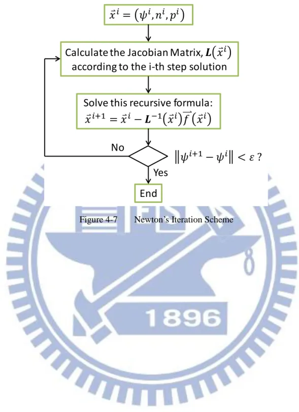
4.5.2 Newton’s Method
The aforementioned weak point of Gummel’s Iteration method can be easily resolved by Newton’s method [21], which is a commonly used method for solving nonlinear equations.
First of all, we may point out that all of 𝑓1, 𝑓2, and 𝑓3 are smoothly varying around the
converged values of (𝜓, , 𝑝) to the change of these independent variables as long as the discontinuity (the correction of the collision term to the relaxation approximation) is moderate. That is, we can linearize (91) – (93) around the converged values of the independent variables. This is the essential meaning of Newton’s Method. Here let us consider the linearization at the (𝑖 + )-th step. The coupled equations of (91) – (93) are divided into the term of 𝑖-th step and the linear deviation therefrom is as follows:
( 𝑓1( 𝜓𝑖, 𝑖, 𝑝𝑖) 𝑓2( 𝜓𝑖, 𝑖, 𝑝𝑖) 𝑓3( 𝜓𝑖, 𝑖, 𝑝𝑖) ) + [ 𝜕𝑓1 𝜕𝜓 𝜕𝑓1 𝜕 𝜕𝑓1 𝜕𝑝 𝜕𝑓2 𝜕𝜓 𝜕𝑓2 𝜕 𝜕𝑓2 𝜕𝑝 𝜕𝑓3 𝜕𝜓 𝜕𝑓3 𝜕 𝜕𝑓3 𝜕𝑝 ] ( ∆𝜓𝑖 ∆ 𝑖 ∆𝑝𝑖 ) = 0. (94)
29
The problem that we will solve is thereby turned out to be a simultaneous linear equation:
𝑳(𝑥⃑𝑖+1− 𝑥⃑𝑖) = −𝑓⃑(𝑥⃑𝑖), (95)
where 𝑓⃑ = (𝑓1, 𝑓2, 𝑓3)𝑡, 𝑥⃑𝑖 = ( 𝜓𝑖, 𝑖, 𝑝𝑖)𝑡, and the Jacobian matrix is:
𝑳 = [ 𝜕𝑓1 𝜕𝜓 𝜕𝑓1 𝜕 𝜕𝑓1 𝜕𝑝 𝜕𝑓2 𝜕𝜓 𝜕𝑓2 𝜕 𝜕𝑓2 𝜕𝑝 𝜕𝑓3 𝜕𝜓 𝜕𝑓3 𝜕 𝜕𝑓3 𝜕𝑝 ] (96) = [ ∇2 −𝑞 𝜖 𝑞 𝜖 ∇ ∙ (−𝑞 𝜇𝑛∇) ∇ ∙ [(−𝑞𝜇𝑛∇𝜓 + 𝑞𝐷𝑛∇)] − 𝜕(𝐺𝑛− 𝑅𝑛) 𝜕 − 𝜕(𝐺𝑛− 𝑅𝑛) 𝜕𝑝 ∇ ∙ (−𝑞𝑝𝜇𝑝∇) − 𝜕(𝐺𝑝− 𝑅𝑝) 𝜕𝑝 ∇ ∙ [(−𝑞𝜇𝑝∇𝜓 − 𝑞𝐷𝑝∇)] − 𝜕(𝐺𝑝− 𝑅𝑝) 𝜕𝑝 ] . (97)
Here we assume that 𝑁𝐷+ and 𝑁𝐴− are constant with regard to any change of (𝜓, , 𝑝) for simplicity. However, the ionization rates of doping atoms are not constant. Actually, we need to take the differentiation of the ionization rates [22, 24, 25] into consideration. The brief algorithm is illustrated in Figure 4-7. Here we start with the last update of the vector 𝑥⃑𝑖, i.e., the last updated set of the independent variables. Next, we calculate the elements of the Jacobian matrix at the last update. Subsequently, we substitute the Jacobian matrix into the recursive formula:
𝑥⃑𝑖+1 = 𝑥⃑𝑖− 𝑳−1(𝑥⃑𝑖)𝑓 ⃑⃑⃑⃑(𝑥⃑𝑖), (98)
to obtain the next update, i.e., 𝑥⃑𝑖+1. Finally, it is noteworthy to say that Newton’s iteration scheme is preferable when the couplings between equations are deeper, while more computer resource is required for calculating the Jacobian matrix.
30