國立交通大學
材料科學與工程學系
博士論文
探討金及硒化鎘奈米粒子自身組織排列於
PS-b-P4VP 雙塊式高分子薄膜之 P4VP 區塊中
之集合電子傳導性質
Collective Electron Transport in Au and CdSe
Nanoparticles Self-Assembled in the
Poly(4-vinylpyridine) Nanodomains of a
Poly(styrene-b-4-vinylpyridine) Diblock Copolymer
Thin Film
研究生: 李中斌 (Chung-Ping Li)
指導教授: 韋光華 (Kung-Hwa Wei)
Abstract
In this dissertation, thin films that consisted of Au and CdSe nanoparticles (NPs), self-assembled in a poly(4-vinylpyridine) (P4VP) nanodomain of poly(styrene-b-4-vinylpyridine) (PS-b-P4VP) diblock copolymer were prepared by polar interaction and solvent selectivity. Collective electron transport of these organic nanodomain confined nanoparticles were investigated.
From conductive atomic force microscopy and device measurements, we found that the electron tunneling rate constant in the case of CdSe quantum dots confined in a P4VP nanodomain is much larger than that in the randomly-distributed case. The calculated electron tunneling coefficient for hopping between confined CdSe quantum dots was 0.3 1/A. The conductivity of the CdSe/P4VP nanodomain increased upon increasing the amount of CdSe, following a percolation model (Chapter 2).
From the current–voltage characteristics of PS-b-P4VP thin films that consist of Au NPs, we found that the collective electron transport behavior of Au NPs sequestered in the spherical P4VP nanodomains was dictated by Coulomb blockade and was quasi one-dimensional, as opposed to the three-dimensional behavior displayed by Au NPs that had been dispersed randomly in homo-P4VP (Chapter 3).
Moreover, CdSe nanorods self-assembled in the P4VP nanodomains of a PS-b-P4VP diblock copolymer thin film were aligned under the influence of the polarization forces created by an applied electric field. The electron mobilities of CdSe/P4VP nanodomains incorporating the out-of-plane CdSe nanorods were much larger than those incorporating in-plane nanorods (chapter 4).
摘要
此論文主旨為利用有機 PS-b-P4VP 雙塊式高分子薄膜自身組織成週期性結 構的特性作為模版並以選擇性分散之技術,分別將無機Au、CdSe 奈米粒子侷限 於P4VP 奈米區塊中形成特定結構之奈米陣列,並探討此具有奈米侷限效應之奈 米粒子之群體電子傳導特性。 利用導電的原子力顯微鏡及電性量測儀器,針對於具有奈米侷限效應之 CdSe 量子點/P4VP 奈米區塊進行量測,發現電子在此具奈米侷限效應之量子點 間之傳導速度遠較不具侷限效應之量子點之傳導速度快。 利用低溫電性量測儀器,針對於具有奈米侷限效應之Au 奈米粒子/P4VP 奈 米區塊進行量測,在78K 之低溫量測下,Au 奈米粒子具有庫侖阻塞效應,進而 發現具有奈米侷限之奈米粒子呈現出趨近於一維電子傳導之特性。 此外,將CdSe 奈米柱選擇性分散於 P4VP 奈米區塊中並在高溫下加入電場 作為驅動力,製備出具方向性且大面積規則排列之 CdSe/P4VP 陣列,並量測加 入電場前後之電子遷移速率。Table of Content
Abstract ... Ⅰ 摘要... Ⅱ Chapter 1: Introduction 1-1 Block Copolymers ...1 1-2 Nanostructured Materials ...121-3 Motivation and Scope of Dissertation ...21
Chapter 2: Basic Electron Transport Theory 2-1 Introduction...48
2-2 Conduction Mechanisms ...48
2-3 Alkanethiol Self-assembled Monolayers Metal-Insulator-Metal Tunneling ...49
Chapter 3: Enhanced Collective Electron Transport by CdSe Quantum Dots Self-Assembled in the Poly(4-vinylpyridine) Nanodomains of a Poly(styrene-b-4-vinylpyridine) Diblock Copolymer Thin Film 3-1 Introduction ...54
3-2 Methods and Analysis ...55
3-3 Results and Discussions ...57
3-4 Conclusions ...65
Chapter 4: Collective Electron Transport in Au Nanoparticles Self-Assembled in the Poly(4-vinylpyridine) Nanodomains of a Poly(styrene-b-4-vinylpyridine) Diblock Copolymer Thin Film 4-1 Introduction ...75
4-2 Methods and Analysis ...76
4-3 Results and Discussions ...78
4-4 Conclusions ...83
Chapter 5: The Orientation of CdSe Nanorods Affects the Electron Mobility of CdSe/P4VP Nanodomains Self-Assembled within a Poly(styrene-b-4-vinylpyridine) Diblock Copolymer Thin Film 5-1 Introduction ...93
5-3 Results and Discussions ...96
5-4 Conclusions ...101
Chapter 6: Conclusions ...109
Figure List
Chapter 1: Introduction
Figure 1-1-1 Schematic phase diagram showing the various ‘classical’ block
copolymer morphologies adopted by linear diblock copolymer...24
Figure 1-1-2 Schematic of morphologies for linear ABC triblock copolymer. A
combination of block sequence (ABC, ACB, BAC), composition and block molecular weights provides an enormous parameter space for the creation of new morphologies ...25
Figure 1-2-1 The well-known structures of block copolymers in melt, solution or
solid state ...26
Figure 1-3-1 Schematic of various applications of block copolymers in
nanotechnologies...27
Figure 1-3-2 Schematic of the production process of a metal nanodot array using
block copolymer lithography ...28
Figure 1-3-3 SEM image of polystyrene-b-polyferrocenyldimethylsilane mask, after
the polystyrene has been removed by O2 RIE ...29 Figure 1-3-4 Schematic representation of high density nanowire fabrication in a
polystyrene-b-poly(methylmethacrylate) matrix ...30
Figure 1-3-5 The morphological transformation from a hexagonally packed cylinder
structure of pure polystyrene-b-poly(4-vinylpyridine) (PS-b-P4VP) diblock
copolymers to lamellar (CdS/P4VP)-b-PS composites...31
Figure 1-3-6 Schematic ofselectived distribution of TiO2 nanoparticles in
polystyrene-b-poly(methylmethacrylate) diblock copolymer...32
Figure 1-3-7 (a) Secondary electron SEM image of the surface of a thin film of a
diblock copolymer–CdSe nanoparticle mixture spin-coated onto a silicon wafer and annealed at 170 ℃ for 2 days (image width, 250 nm) taken at 1-kV acceleration voltage. (b) Schematic representation of nanoparticle assembly at the
Figure 1-3-8 TEM micrograph of a ternary blend of polystyrene-b-poly(ethylene
propylene) + AuR1 + SiO2R2 with inorganic filling fraction f = 0:02; respectively, after micro-sectioning normal to the layer direction (no stain) ...34
Figure 1-3-9 (a) Assembly of Au nanoparticles (core: 3.9 ± 1.0 nm; shell: polystyrene;
(core+shell)=7.7 nm) into polystyrene-b-poly(2-vinylpyridine) diblock copolymers. (b) Assembly of Au nanoparticles (core: 3.9 ± 1.0 nm; shell: polystyrene and
poly(2-vinylpyridine); (core+shell)=7.7 nm) into polystyrene-b-poly(2-vinylpyridine) diblock copolymers. (c), (d) The respective histograms of particle locations for the samples shown in (a) and (b). Reprinted with permission...35
Figure 1-3-10 Cross-sectional transmission electron micrograph showing Au
nanoparticles patterned within the poly(4-vinylpyridine) lamellae formed by a polystyrene-b-poly(4-vinylpyridine) diblock copolymer ...36
Figure 1-3-11 Schematic of synthesis of needle-like TiO2 nanostructures with ordered patterns...37
Figure 1-3-12 SEM image of an etched polystyrene-b-polyisoprene diblock, showing
a fracture surface. The polystyrene network channels remaining after removal of polyisoprene are clearly visible ...38
Figure 1-4-1 Schematic illustration the density of state in semiconductors. ...39 Figure 1-4-2 EL spectra collected on ITO/PPV (400 Å)/CdSe(CdS)/Mg/Ag devices
having average nanocrystal layer thicknesses of 100 (a), 200 (b), and 400 Å (c). (d) Show the voltage dependence of the ratio of integrated nanocrystal EL to integrated PPV EL for the device shown in (b) ...40
Figure 1-4-3 (a) The structure of regioregular P3HT. (b) The schematic energy level
diagram for CdSe nanorods and P3HT showing the charge transfer of electrons to CdSe and holes to P3HT. (c) The device structure consists of a film ;200 nm in thickness sandwiched between an aluminum electrode and a transparent conducting electrode of PEDOT:PSS...41
Figure 1-4-4 I-V curve of Al/Au-2NT NPs+PS/ Al. The arrows indicate the
Figure 1-4-5 (a) SEM image of a chain consisting of three Au nanoparticles
incorporated in a system of source, drain, and gate metal electrodes. (b) Scheme of electrode pattern defined by electron beam lithography. (c) Drain current (ID) versus source-drain voltage (VSD) characteristics of the SET transistor measured at 4.2 Kwith various gate voltages (VG) ...43
Figure 1-4-6 (a) Preparation of “nanocrystal molecules” consisting of two or three
DNA modified Au particles attached to a complementary DNA template. (b) TEM images of the binary AuNPs network materials supported on holey carbon grids....44
Figure 1-4-7 Schematic of a threshold voltage proportional to the linear array size
...45
Figure 1-4-8 (a) Representative TEM images of Au nanoparticles /silica mesophases.
(b) I-V curves measured from 300 K to 78 K. The inset plots the zero-bias conductance (G0) versus 1/T. (c) At T = 78 K, current displays a power-law dependence for V > VT with scaling exponent ζ= 2.7 (negative bias) andζ= 3.0 (positive bias)...46
Figure 1-4-9 (a) SEM image of self-assembled Co nanoparticles superlattice device
(b) Device I-V characteristic, for T= 2 K (dark line) and 20, 40, and 70 K (light lines). (Inset) Plot of zero-bias conductance versus 1/T. (c) For V > VT, current displays a power-law dependence...47
Chapter 2: Basic Electron Transport Theory
Figure 2-1 E-k relationship (symbols) generated from the length-dependent
measurement data for alkanethiols.···53
Chapter 3: Enhanced Collective Electron Transport by CdSe Quantum Dots Self-Assembled in the Poly(4-vinylpyridine) Nanodomains of a
Poly(styrene-b-4-vinylpyridine) Diblock Copolymer Thin Film
Figure 3-1 (a) TEM image of a thin film of 48% (CdSe/P4VP)-b-PS obtained without
employed. (c) Conductive-AFM image of a thin film of 48% (CdSe/P4VP)-b-PS. ...70
Figure 3-2 (a) I–V curves of thin film (CdSe/P4VP)-b-PS by conductive-AFM. The
dotted lines denote best fits to the FN equation. Inset: The energy bands of the conductive-AFM tip, CdSe/P4VP monolayer, and the substrate. Ef is the electron Fermi energy inside the Pt, and φe is the barrier height between Pt and CdSe/P4VP.
eVa is the applied potential energy difference between the tip and the substrate. (b) Plot of the conductivity vs. the amount of CdSe in P4VP. ...71
Figure 3-3 (a) Plot of –ln(σ(CdSe/P4VP)-b-PS) vs. δe as measured by conductive-AFM and device. (b) Schematic diagram of the barrier height for electron tunneling from the conduction band of CdSe to the LUMO of P4VP and from the Fermi level of Au to the LUMO of an alkanethiol...72
Figure 3-4 (a) Iave–V curves of thin film (CdSe/P4VP)-b-PS nanocomposites having various contents of CdSe as measured in a device. The dotted lines denote best fits to the FN equation. (b) Plot of the conductivity vs. the amount of incorporated CdSe in P4VP. ...73
Figure 3-5 (a) Small-angle X-ray scattering of bulk (CdSe/P4VP)-b-PS
nanocomposites having various contents of CdSe. (b) A schematic representation of the cubic lattice model for the free volume per CdSe dot in a single P4VP domain...74
Chapter 4: Collective Electron Transport in Au Nanoparticles Self-Assembled in the Poly(4-vinylpyridine) Nanodomains of a Poly(styrene-b-4-vinylpyridine) Diblock Copolymer Thin Film
Figure 4-1 (a) Conventional, (b) high-resolution, and (c) cross-sectional TEM images,
obtained without staining, of a thin film of 48% (Au NPs/P4VP)-b-PS. ...86
Figure 4-2 I–V curves of (a) 48% (Au NPs/P4VP)-b-PS and (b) Au NPs/homo-P4VP
thin films measured at temperatures between 250 and 78 K. (c) Scaling behavior of the I–V curves of 48% (Au NPs/P4VP)-b-PS and Au NPs/homo-P4VP at 78 K. (d) Plots of VT vs. d for the 48% (Au NPs/P4VP)-b-PS and Au NPs/homo-P4VP samples
having various contents of Au NPs...87
Figure 4-3 (a) Small-angle X-ray scattering of bulk (Au NPs/P4VP)-b-PS
nanocomposites having various contents of Au NPs. (b) Schematic representation of the cubic lattice model for the free volume per Au nanoparticle in a single P4VP domain. ...89
Figure 4-4 I–V Curves measured at 78 K for (Au NPs/P4VP)-b-PS and Au NPs/P4VP
thin films. Details of the fitting and determination of the threshold voltages and scaling exponents are provided in the corresponding tables...90
Figure 4-5 (a) I–V Curves, measured at 78 K, of (Au NPs/P4VP)-b-PS thin films
having various contents of Au NPs. (b) Scaling behavior of the I–V curves of (Au NPs/P4VP)-b-PS having various contents of Au NPs at 78 K. ...91
Figure 4-6 (a) I–V Curves, measured at 78 K, of Au NPs/homo-P4VP thin films
having various contents of Au NPs. (b) Scaling behavior of the I–V curves of Au NPs/homo-P4VP having various contents of Au NPs at 78 K...92
Chapter 5: The Orientation of CdSe Nanorods Affects the Electron Mobility of CdSe/P4VP Nanodomains Self-Assembled within a
Poly(styrene-b-4-vinylpyridine) Diblock Copolymer Thin Film
Figure 5-1 TEM images, obtained without staining, of thin films of (a) 65%, (b) 48%,
and (c) 33% (CdSe/P4VP)-b-PS. ...104
Figure 5-2 SEM images of 33% (CdSe/P4VP)-b-PS thin films prepared (a) in the
absence and (b) in the presence of an applied electric field. ...105
Figure 5-3 Cross-sectional TEM images of 33% (CdSe/P4VP)-b-PS thin films
prepared (a) in the absence of and (b) in the presence of an applied electric field. The insets display the respective HRTEM lattice images of a CdSe NR incorporated within a single P4VP nanodomain of (CdSe/P4VP)-b-PS. (c) A schematic depiction of the electron transport process. ...106
Figure 5-4 Averaged current density–electric field (J–E) curves of a single
out-of-plane and (b) in-plane CdSe NRs. The dashed lines denote best fits to the FN equation; the dotted lines denote best fits to the SCLC model, which includes the field-dependent mobility...107
Figure 5-5 Orientation angle of the protruded CdSe NRs with respect to the plane of
Scheme & Table List
Chapter 2: Basic Electron Transport Theory
Table 2-1 Possible conduction mechanisms.···52
Chapter 3: Enhanced Collective Electron Transport by CdSe Quantum Dots Self-Assembled in the Poly(4-vinylpyridine) Nanodomains of a
Poly(styrene-b-4-vinylpyridine) Diblock Copolymer Thin Film
Scheme 3-1 Fabrication of a self-assembled (CdSe/P4VP)-b-PS thin film by
incorporating selectively dispersed pre-synthesized CdSe QDs in P4VP domain... 66
Table 3-1 Conductivity (σ ) and electron tunneling rate constant (kET) for confined
and non-confined CdSe in P4VP domain as measured by conductive-AFM and in a device ...67
Table 3-2 Characteristic Properties of CdSe Quantum Dots ...68 Table 3-3 Electrical conductivity parameters for the CdSe/P4VP nanodomain...69
Chapter 4: Collective Electron Transport in Au Nanoparticles Self-Assembled in the Poly(4-vinylpyridine) Nanodomains of a Poly(styrene-b-4-vinylpyridine) Diblock Copolymer Thin Film
Scheme 4-1 Fabrication of a self-assembled (Au NPs/P4VP)-b-PS thin film through
the selective incorporation of dispersed pre-synthesized Au NPs into P4VP domains. ...84
Table 4-1 Details of the Fitting of I–V Curves, Measured at 78 K, for (Au
NPs/P4VP)-b-PS and Au NPs/P4VP Thin Films Having Various Contents of Au NPs, and Determination of the Threshold Voltages and Scaling Exponents...85
Chapter 5: The Orientation of CdSe Nanorods Affects the Electron Mobility of CdSe/P4VP Nanodomains Self-Assembled within a
Poly(styrene-b-4-vinylpyridine) Diblock Copolymer Thin Film
Scheme 5-1 Fabrication of a self-assembled (CdSe/P4VP)-b-PS thin film through the
selective incorporation of dispersed pre-synthesized CdSe NRs into P4VP
Table 5-1 Electron barrier heights (φe), electron mobilities (µ0), and field
coefficients (E )0 for in-plane and out-of-plane CdSe NRs incorporated within P4VP
Chapter 1 Introduction
1-1 Block Copolymers
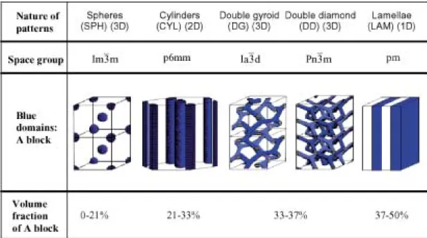
A block copolymer (BCP) can self-assemble into an ordered periodic structures with a nanometer thicknesses that depends on molecular weight, segment size, and the strength of interaction between the blocks, represented by the Flory–Huggins interaction parameter,
χ
. [1–3] The periodicity thickness is in the range 10–200 nm.The morphology depends on
χ
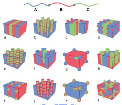
and the composition of the copolymer, parametrized as the volume fraction of one of the constituent blocks. For the simplest class of A-B diblock copolymers, the following structures are known to be stable, as confirmed by theory [4] and experiment [2, 5]: lamellar, hexagonal-packed cylinder, body-centred cubic, close-packed spherical (which may exhibit only liquid-like ordering) and bicontinuous cubic gyroid structures, as shown in Figure 1-1-1. For ABC triblocks, the combination of two independent composition variables (e.g. volume fraction fA and fB, fA+ fB+ fC = 1) and threeχ
parameters (χ
AB,χ
ACand
χ
BC) leads to a much wider range of possible morphologies shown in Figure 1-1-2. Many have been observed, although others await discovery. [6] Theory provides guidelines for rationalizing the observed morphologies, and in the future may be used to predict structures. [7]1-1-1 The Structure of Block Copolymer melts, solids, and solutions
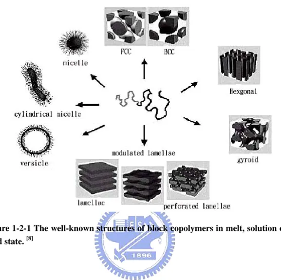
A remarkable property of block copolymers is their ability to self-assemble in the melt in to a variety of ordered structures with nanoscale periodicities. These structures can be controlled by varying the composition of the block copolymer or the segregation between blocks (via temperature or degree of polymerization). In addition to the now well-established lamellar (lam), hexagonal-packed cylinder(hex)
and body-centered cubic (BCC) micelle phase, a number of few morphologies have been discovered, which supplement the “classical structure”. The identification of a bicontinuous cubic phase of Ia3d symmetry, sometimes called the gyroid phase, is
now established. Figure 1-2-1 shows the well-known structure of block copolymers in melt, solution or solid state. [8]
Melts
Two competing effects govern the thermodynamics of block copolymer melts. At high temperature, the chains are mixtures homogeneously, as in any polymer melt. As the temperature is reduced, the tendency for the blocks to segregate is enhanced, i.e. the enthalpic process of demixing is favored. However, this is necessarily accompanied by a reduction in entropy as the chain configuration becomes more constrained. The extent of segregation of the copolymer may then be expressed using the reduced parameter
χ
N. Here N is the copolymer degree of polymerizatiom, reflecting the N-dependent translation and configuration entropy.The segment–segment interaction parameter (Flory–Huggins) described the free energy cost per monomer of conducts between the A and B monomeric units and is given by:
[
AB(
AA BB)
/2]
B AB Zκ T ε ε ε χ − + = , where εABis the interaction energy
permonomer units between A and B monomers and Z is the number of nearest neighbor monomers to a copolymer configuration cell. Thus, positive
χ
AB (whichis the vast majority of cases) shows repulsion between the A and B monomers, whereas a negative value signifies mixing of unlike monomers. Moreover,
χ
ABusually varies inversely with temperature. The second parameter that strongly influences the block copolymer behavior is the total degree of polymerization N. For large N the loss of translational and configurational entropy leads to a reduction
of the A-B monomer contacts and thus to local ordering. Since the entropic and enthalpic contributions to the free energy scale as N-1 and
χ
, respectively, it is theproduct
χ
N that is of interest in the block copolymer phase state.Solutions
There are two basic processes that characterize the phase behavior of block copolymers in solution: micellization and gelation. Micellization occurs when block copolymer chains associate into, often spherical, micelles in dilute solution in a selective solvent. The core of the micelle is formed by the insoluble or poorly solvated block, whilst the corona contains the selectively solvated block. At a fixed temperature, micellization occurs on increasing concentration at the critical micelle concentration (CMC). The cmc is usually determined from the sharp decrease in the surface tension as a function of concentration, although other properties such as viscosity also exhibit pronounced changes.
In concentrated solutions, micelles can order into gels. Soft and hard gels are distinguished from each other and from micellar solutions by their flow properties, gels being characterized by a finite yield stress. The hard gels seem to be associated with the formation of cubic phases of spherical micelles, whereas soft gels are usually lamellar or hexagonal-packed rod micellar phase. The phase behavior of these materials has only recently begun to be elucidated using small angle scattering. It promises to be even richer than that of block copolymer melts, at least if results for analogous conventional surfactants are any guide. The flow behavior of these gels is the basis for many of their applications, and study of the rheology and behavior under shear of these materials will enhance the fundamental understanding underpinning future developments.
The structure of block copolymer melts is usually trapped upon vitrification. The mechanism underlying the glass transition are similar to those of the constituent homopolymers. Thus there are little distinct physicals associated with the formation of solid phase by glassy block copolymers.
In contrast, crystallization of one or both components of a block copolymer is accompanied by profound structure and dynamic changes. The fundamental process in crystallization of chains in a crystallizable block copolymer is the change in block conformation, i.e. the adoption of an extended or a folded structure rather than a coiled configuration found in the melt or solution. Crystallization from the melt often leads to a distinct (usually lamellar) structure, with a different periodicity from the melt. Crystallization from solution can lead to non-lamellar crystalline structures, although these may be often be trapped non-equilibrium morphology. In addition to the formation of extended or folded chains, crystallization may also lead to gross orientational changes of chains.
1-1-2 Applications
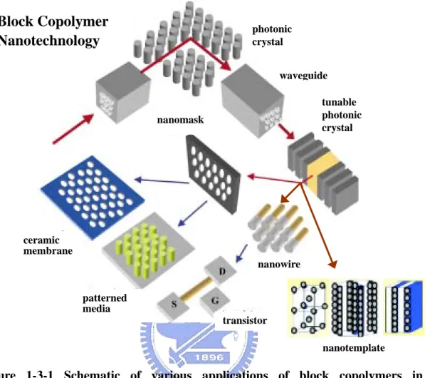
Until recently, most industrial applications of BCPs were as adhesives or for their mechanical properties (e.g. as thermoplastic elastomers). Only in the past 10 years have researchers taken BCPs into the “high-technology” area, to the so-called “nanotechnologies”. Many attempts have been made to utilize BCPs in nanotechnology. Self assembled BCP microstructures with 10 to 100 nm dimensions are useful as nanometer scale membranes, templates for fabrication of nano-objects such as metal, ceramic nanodots and wires, as 1-, 2- and 3D photonic crystals, and as nanopattern masks for fabrication of high density information storage media. The majority of applications proposed to date rely on the use of thin film structures and this is a major focus of the current review, although bulk nanoporous materials and photonic crystals are considered. The applications of various BCP
enabled nanotechnologies are summarized in Figure 1-3-1. [9]
Nanolithography
Nanosizes greater than 150 nm can be routinely produced by photolithography techniques. The minimum size that can be achieved by photolithography is determined by the wavelength of light used in the exposure. Electron beam lithography is commonly used to access feature sizes between 150 nm and 30 nm. However, sizes less than 30 nm are not easily obtained by standard lithography. One way to overcome this problem is by using self-assembled block copolymers.
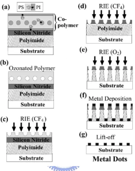
In a pioneering paper, Park et al [10] demonstrated the use of block copolymer films as masks to transfer dot and stripe patterns into semiconductors. The feature density of holes achieved was ~1011 cm -2. The method they developed relies on the selective ozonation of polyisoprene (PI) or polybutadiene (PB) in block copolymers with polystyrene (PS) as the other, majority, component. Ozone cleaves the double bonds in the unsaturated polymers, so that they can be etched away. This process leaves holes or stripes in a PS matrix. This pattern was transferred from the block copolymer into silicon nitride by RIE using CF4 or CF4/O2 gases. The quality of pattern transfer is excellent, producing nanoscale arrays of pits or channels. Park et
al also discuss how to prepare a nanoscale array of posts by use of an “inverse”mask
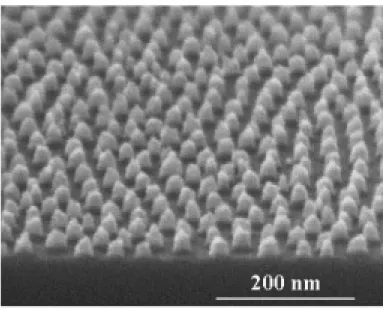
to that used to produce the array of pits. If the PI is fixed by staining with osmium tetroxide, then etching of the matrix will occur preferentially. The regions under the PI domains will be left as an array of posts. Details of the ozone etching method of preparing block copolymer film masks were elaborated on in a subsequent paper, [11] which also contains data illustrating pattern transfer into other semiconductors, including silicon and germanium. A patent was awarded for this technology in 1999. [12] In a further extension of the technique, it has been demonstrated that arrays of nano-sized metal posts can be fabricated, by an extension of the preceding method,
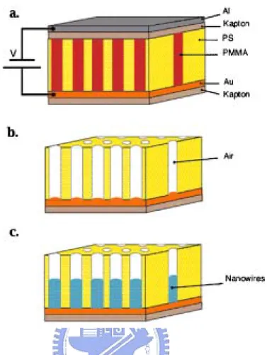
illustrated in figure 1-3-2. [13] A lithographic procedure in which the ozone etching step can be omitted has also been demonstrated. [14] Here the reactive ion etch rate is sufficiently different between the two blocks in a PS-b-PFS (PFS = polyferrocenyldimethylsilane) diblock, for selective etching of PS to occur directly. The application again was the development of a self-assembly route to produce a high-density magnetic storage medium (in this case cobalt nanodots). O2 RIE leaves PFS spheres, the pattern then being transferred into silicon oxide (which improves pattern transfer) then into tungsten by RIE. The multiplayer structure is necessary because magnetic materials, such as cobalt, nickel and iron are not amenable to RIE. In the next step, the polymer and silica are removed. Finally, the pattern is transferred from the tungsten hard mask into the magnetic cobalt layer using ion-beam etching. The result is the array of cobalt nanoposts illustrated in figure 1-3-3. Ultrahigh-density metal nanocolumn arrays can be fabricated using block copolymer templates. Russell et al [15] oriented the poly(methylmethacrylate) (PMMA) cylinders in a PS-b-PMMA diblock by applying an electric field across the polymer film (Figure 1-3-4(a)). The PMMA was then degraded by deep UV radiation, which simultaneously cross-links the PS. The degraded PMMA was removed by acid rinsing. The resulting array of nanopores (Figure 1-3-4(b)) was subsequently filled with cobalt by electrodeposition from a methanol solution. Due to the size of the nanowires, single magnetic domain behaviour was anticipated, with obvious potential in patterned magnetic storage media (Figure 1-3-4(c)). The magnetic behavior was also highly anisotropic, with a much larger coercivity field parallel to the wire. The application of the approach to the fabrication of nanoelectrode arrays has also been reported. [16] Russell and coworkers have also used porous PS films, formed from PS-b-PMMA precursors, as masks for pattern transfer (by RIE) into FeF2/Fe bilayers to create magnetic nanostructures. [17]
Nanoparticle Templates
BCPs have also been utilized not only as surfactants to inhibit coalescence and aid in dispersion of nanoscale particles such as metal, metal oxide, inorganics, molecular chromophores and quantum dots but also to spatially pattern the particles.
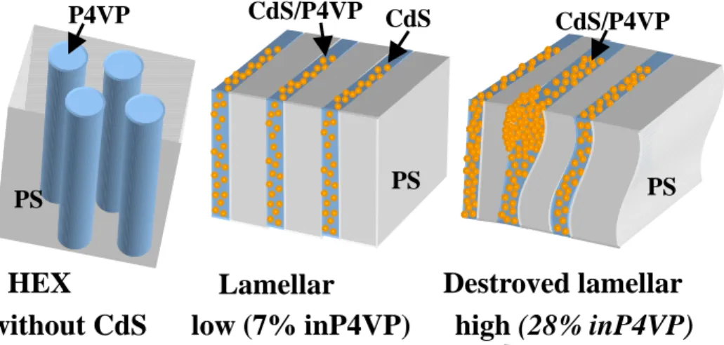
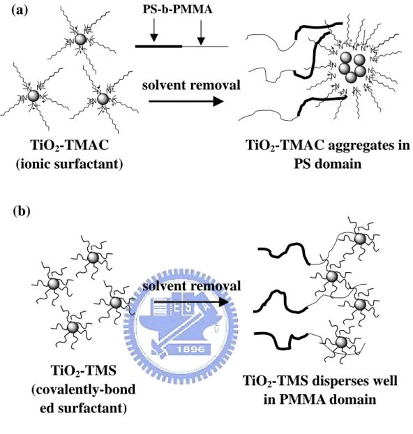
In previous works of our group, we reported a morphological transformation of PS-b-P4VP (P4VP = poly(4-vinylpyridine)) from a hexagonally packed cylinder structure to a lamellar structure, which occurred upon sequestering CdS nanoparticles in the P4VP block. [18] The surface of the CdS nanoparticles was stabilized with mercaptoacetic acid as a surfactant, which renders each CdS nanoparticle hydrophilic. Thus, CdS nanoparticles segregated selectively into the P4VP domains due to the dipole-dipole interactions between the carboxylic acid on the CdS surface and the P4VP chains. Whereas pure PS-b-P4VP showed a hexagonally packed cylindrical structure, the composite transformed into a lamellar structure in the presence of 7 wt% CdS nanoparticles (Figure 1-3-5). The morphological transformation from the cylindrical to lamellar structure was mediated by strong interaction forces such as hydrogen bonds between carboxylic acid units of the CdS nanoparticles and the P4VP chains. In another paper, [19] ordered clusters of surfactant-modified TiO2 nanoparticles in the selective block of lamellar assemblies of the diblock copolymer PS-b-PMMA have been reported (Figure 1-3-6). Instead of using an water or alcohol phase, the TiCl4 or tetra(isopropoxide) (TTIP) precursors were used to synthesize the TiO2 nanoparticles in tetrahydrofuran (THF), which is a good solvent, for block copolymers. Cetyl trimethyl ammonium chloride (TMAC) amphiphilics or 3-(methacryl loyloxypropyl)-trimethoxy silane (TMS) surfactant was used to modify the TiO2 nanoparticles. To our knowledge, this presents a new approach to selectively disperse quantum-confined nanoparticle clusters in a PS-b-PMMA diblock copolymer with an ordered lamellar phase. 3-D and 2-D nanostructure of CdS
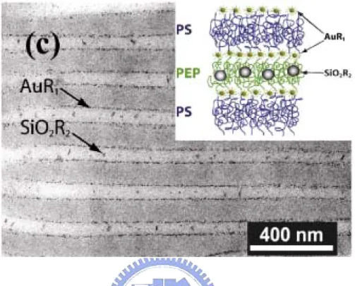
clusters by dispersing pre-synthesized CdS nanoparticles, containing hydroxyl groups on surface, in the PEO block selectively of polystyrene-b-poly(ethylene oxide) (SEO) block copolymers as template in the bulk form and thin films were reported. [20-24] Russell [25] et al. reported that mixtures of diblock copolymers and either cadmium selenide- or ferritinbased nanoparticles exhibit cooperative, coupled self-assembly on the nanoscale. In thin films, the copolymers assemble into cylindrical domains, which dictate the spatial distribution of the nanoparticles; segregation of the particles to the interfaces mediates interfacial interactions and orients the copolymer domains normal to the surface, even when one of the blocks is strongly attracted to the substrate. Organization of both the polymeric and particulate entities is thus achieved without the use of external fields opening a simple and general route for fabrication of nanostructured materials with hierarchical order (Figure 1-3-7). Thomas et al. [26] have identified that the localization of particles along the interface or at the center of the respective polymer domain was also affected by the particle-core sizes. In the system consisting of a symmetric PS-b-PEP (PEP = poly(ethylene propylene)), large silica nanoparticles (d = 21.5 nm; d/L ~ 0.26, where d is the particle diameter and L is the respective domain dimension of the block copolymer) were located at the center of the PEP domain. The smaller gold nanoparticles (d = 3.5 nm, d/L ~ 0.06) segregated at the interface between two block phases (Figure 1-3-8) in accordance with theoretical simulations. [26] Interfacial segregation of nanoparticles is expected to occur for particle sizes with d/L<0.2, whereas localization of nanoparticles at the center of the lamellae phase is expected for d/L>0.3. Figure 1-3-9a shows a cross-sectional TEM image of 100% PS thiol-coated gold nanoparticles dispersed on symmetric PS-b-P2VP block copolymer. [27] PS-coated gold nanoparticles are located near the center of the PS block phase of the lamellae structure, whereas poly(2-vinylpyridine) (P2VP)-coated gold
nanoparticles were located in the P2VP domain as expected. Particles coated with a similar homopolymer can lower their enthalpy by segregating into the corresponding domain of the block copolymer. Positioning the particle near the center of the corresponding polymer domain leads to a better embedding of the NP since the polymer chains can accommodate particles by moving apart rather than by stretching. Particles coated with a mixture of PS and P2VP thiols are exactly localized at the interface between the PS and P2VP block phases (Figure 1-3-9b).
Nanoreactors for nanostructure production
Block copolymer domains can be used as ‘nanoreactors’ for the synthesis of inorganic nanoparticles. Reviews of the subject are available. [28, 29] Two basic approaches have been developed. The first involves the binding of inorganic species to the monomer prior to polymerization or to one of the blocks of a copolymer prior to micellization (which may be induced by the ion binding [28]). The most important approach, however, involves the loading of pre-formed micelles, whether in solution or in bulk.
Micellar nanoreactors for metallic nanoparticles based around several different block copolymers have been investigated by Bronstein and coworkers. In many cases, the ability of poly(vinylpyridine), P2VP or P4VP, to form complexes with metal salts due to the presence of an N atom is exploited. [30–31] For example, palladium clusters have been produced by reduction of Pd(CH3COO)2 that coordinates to the P4VP micellar core formed by PS-b-P4VP diblocks in toluene. [30, 32] Other metal nanoclusters including cobalt, [33] gold, [30, 31, 32] rhodium [30] and platinum [30] have been prepared in a similar way. The catalytic hydrogenation properties of the nanoclusters havebeen compared. [30, 32] Bimetallic colloids have also been prepared. [30] The methods may be extended to thin films where surface interactions may be exploited to prepare highly aligned nanostructures. Sohn and
Seo [34] exploited strong preferential interfacial segregation of the blocks in a thin filmof a PS-b-P4VP diblock to fabricate a multilayer stack consisting of alternating P4VP lamellae containing gold nanoparticles and nanoparticle-free PS lamellae (Figure 1-3-10). Titania nanoparticles are interesting for applications such as catalysis, water purification and UV blocking. Spatz et al [35] have shown how nanoparticles can be produced within block copolymer micelle nanoreactors. They prepared micelles from a PS-b-PEO (PEO = poly(ethylene oxide)) diblock in a non-polar solvent with a PS corona and a PEO core. HCl was mixed with the micelle solution to create reservoirs within the micelle cores. Titanium alkoxides were then added, the reaction with the acid and subsequent heating leading to the formation of TiO2 particles. Individual particles and chains were both obtained. In previous works of our group, we have reported synthesis of arrayed, TiO2 needle-like nanostructures via a PS-b-P4VP diblock copolymer template. [36] Arrayed, needle-like nanostructures of rutile phase crystal TiO2 were grown on a Si substrate containing TiO2 seeds prepared through a thin PS-b-P4VP (use unabbreviated name first) diblock copolymer template. By using TiO2 seeds prepared from their diblock copolymer PS-b-P4VP template, arranged needle-like rutile TiO2 nanostructures with variable spatial positions and densities were fabricated. The distance between two TiO2 needle bunches could be controlled using block copolymer templates with different molecular weights (120nm and 160 nm) (Figure 1-3-11).
Photonic Crystals
Photonic crystals are attracting immense attention since they can be used to control and confine light. Materials with a complete bandgap reflect light (incident in any direction) within the wavelength range of the gap. Block copolymers are interesting materials with which to construct photonic crystals because they can self-assemble into periodic structures in one, two and three dimensions. The
inherently low dielectric contrast between the polymeric domains can be overcome by selective doping and/or removal of one component. Another prime constraint is the requirement for telecommunications applications of a domain size of about 250 nm (to control near-IR radiation with a wavelength of 1.55 μm). [37] Additionally, long-range order of the materials must be achieved. Much of the current research comes from the Thomas group, and they have provided a good review of material requirements and possibilities, as well as research up to year 2000, [37] this is also being complemented by an earlier overview. [38]
Theory has been used to predict the possibility of photonic bandgaps in single and double network bicontinuous cubic structures. [39] However, the calculations indicated that (for the parameter space explored) no complete bandgaps exist for bicontinuous double primitive, double gyroid (body-centred cubic) or double diamond (face-centred cubic) structures. However, bandgaps are anticipated for the single network analogues, the best candidate being a single diamond structure with a dielectric contrast as low as 3.6. The optical reflectivity characteristics of an experimentally realized large domain double gyroid structurewere subsequently assessed. [40] The initial material was a PS-b-PI diblock with high molar mass leading to a cubic lattice parameter a = 258 nm. The optical properties were measured for a bulk film, and also for sample in which the PI block was removed by UV/ozone treatment (Figure 1-3-12), creating an interpenetrating PS network structure. As anticipated by theory, a complete bandgap was not observed, although a wavelength range with high reflectivity was identified. This was shifted to lower wavelength in the etched structure. A fruitful way to enhance the dielectric contrast in such an etched bicontinuous structure may be to coat the nanochannels with metal. Electroless deposition of nickel (using suitable activators) onto PS channels formed
by etching the PI in a bicontinuous PS-b-PI morphology (with PS homopolymer) has been carried out successfully. [41]
1-2 Nanostructured Materials
Colloidal nanocrystals are sometimes referred to as “artificial atoms” because the density of their electronic states — which controls many physical properties — can be widely and easily tuned by adjusting the crystalۥs composition, size and shape. The combination of size- and shape-dependent physical properties and ease of fabrication and processing makes nanocrystals promising building blocks for materials with designed functions. [42,43] But the ability to control the uniformity of the size, shape, composition, crystal structure and surface properties of the nanocrystals is not only of technological interest: access to defined nanoscale structures is essential for uncovering their intrinsic properties unaffected by sample heterogeneity. Rigorous understanding of the properties of individual nanocrystals will enable us to exploit them, making it possible to design and build novel electronic, magnetic and photonic devices and other functional materials based on these nanostructures. Figure 1-4-1 shows variation of states of electrons with increase the quantization dimension in quantum structure.
1-2-1 Semiconductor Nanoparticles
Characteristics of Semiconductor Nanoparticles
Semiconductor nanoparticles have an inorganic core that is stabilized by a layer of surface surfactants. Nanoparticles with a semiconductor as the inorganic material — so-called quantum dots — exhibit size-tunable band gaps. Shape control of such colloidally prepared nanostructures has been recently achieved by modifying the synthesis to obtain rod shaped particles—nanorods.
Quantum dots have two obvious characteristics. One is the surface area effect and the other is quantum confinement effect. In surface area effect, for particles in such a small size regime, a large percentage of the atom is on or near the surface, for example, 99% of the atoms are on the surface for a 1nm size particles. [44] The existence of this vast interface between the nanoparticles and the surrounding medium can have a profound effect on the particles properties. The imperfect surface of the nanoparticles may act as electron and/or hole traps upon optical excitation. Thus the presence of these trapped electrons and holes can in turn modify the optical properties of the particles. In quantum confinement effect, “confinement” and “quantization” are two closely related definition: If a particles is “confined” then its energy is “quantized”, and vice versa. According to the dictionary, to “confine” mean to “restrict within limits” to “enclose”, and even to “imprison”. The quantum confinement not only causes the increase of the energy gap (blue shift of the absorption edge) and the splitting of the electronic states, but also changes the densities of state and the exciton oscillator strength. [45] It was revealed that many of the differences between the electronic behaviors of the bulk and the quantum-confined low-dimensional semiconductors are due to their difference densities of state.
Nanorods exhibit electronic and optical properties that differ from quantum dots. For example, unlike the spherical dots, nanorods demonstrate linearly polarized
emission [46, 47] leading also to polarized lasing. [48] In addition to size and shape, nanocrystals’ charging may also significantly influence their electrical and optical
properties. Millo et al. reported optical and tunneling spectroscopies on CdSe nanorods and correlated the experimental data with the level structure calculated using a multi-band effective-mass model for an infinite potential well.[49] However, the experimental set-up in both optical and tunneling measurements was tuned so as to avoid nanorods charging.
Applications of CdSe Nanoparticles
In 1993, a paper entitled “Synthesis and Characterization of Nearly Monodisperse CdX (X=S, Se, Te) Semiconductor Nanoparticles” by Murray, Norris, and Bawendi appeared in the Journal ofthe American Chemical Society. [50] CdSe nanoparticles are (potential) building blocks for new electronic and optical nanodevices such as light-emitting diodes, solar cells, lasers, and biological labels.
Light-emitting diodes Alivisatos et al. reported improved efficiencies in light
emitting diodes made with CdSe (CdS) core/shell type nanoparticles and a semiconducting polymer. [51] They reported experiments on bilayer light emitting diodes made with organically capped CdSe(CdS) core/shell type semiconductor nanoparticles and an electroluminescent (EL) semiconducting polymer poly(p-phenylenevinylene) (PPV). The devices emit from red to green with external quantum efficiencies of up to 0.22% at brightnesses of 600 cd/m2 and current densities of 1 A/cm2. They have operating voltages as low as 4 V and lifetimes under constant current flow of hundreds of hours. Most of these numbers are significant improvements over similar devices made with CdSe nanoparticles. The devices show either nanoparticle-only EL or a combination of nanoparticle and PPV EL, depending on nanoparticle layer thickness. The nanoparticle EL is dependent on nanoparticle size. Some devices show a voltage dependent spectral output. The spectral output is consistent with a field dependent electron range in the nanoparticle layer limited by carrier trapping (Figure 1-4-2).
Solar cells Alivisatos et al. reported hybrid CdSe nanorods-conjugated polymer
solar cells. [52] They demonstrated that semiconductor nanorods can be used to fabricate readily processed and efficient hybrid solar cells together with polymers. By controlling nanorod length, we can change the distance on which electrons are transported directly through the thin film device. Tuning the band gap by altering
the nanorod radius enabled us to optimize the overlap between the absorption spectrum of the cell and the solar emission spectrum. A photovoltaic device consisting of 7-nanometer by 60-nanometer CdSe nanorods and the conjugated polymer poly-3(hexylthiophene) was assembled from solution with an external quantum efficiency of over 54% and a monochromatic power conversion efficiency of 6.9% under 0.1 milliwatt per square centimeter illumination at 515 nanometers. Under Air Mass (A.M.) 1.5 Global solar conditions, we obtained a power conversion efficiency of 1.7% (Figure 1-4-3).
Lasers Bawendi et al. reported optical gain and stimulated emission in
semiconductor nanoparticles. [53] The development of optical gain in chemically synthesized semiconductor nanoparticles has been intensely studied as the first step toward semiconductor nanoparticles lasers. They examined the competing dynamical processes involved in optical amplification and lasing in semiconductor nanoparticles and found that, despite a highly efficient intrinsic nonradiative Auger recombination, large optical gain can be developed at the wavelength of the emitting transition for close-packed solids of these nanoparticles. Narrowband stimulated emission with a pronounced gain threshold at wavelengths tunable with the size of the semiconductor nanoparticle was observed, as expected from quantum confinement effects. These results unambiguously demonstrate the feasibility of nanocrystal quantum dot lasers.
Biological labels Alivisatos et al. reported semiconductor nanoparticles as
fluorescent biological labels. [54] Semiconductor nanoparticles were prepared for use as fluorescent probes in biological staining and diagnostics. Compared with conventional fluorophores, the nanoparticles have a narrow, tunable, symmetric emission spectrum and are photochemically stable. The advantages of the broad, continuous excitation spectrum were demonstrated in a dual-emission,
single-excitation labeling experiment on mouse fibroblasts. These nanoparticle probes are thus complementary and in some cases may be superior to existing fluorophores.
1-2-2 Metal Nanoparticles
Characteristics of Metal Nanoparticles
Physicists predicted that metal nanoparticles in the diameter range 1-10 nm (intermediate between the size of small molecules and that of bulk metal) would display electronic structures, reflecting the electronic band structure of the nanoparticles, owing to quantum-mechanical rules. [55] The resulting physical properties are neither those of bulk metal nor those of molecular compounds, but they strongly depend on the particle size, interparticle distance, nature of the protecting organic shell, and shape of the nanoparticles. [56] The few “last metallic electrons” are used for tunneling processes between neighboring particles, an effect that can be detected by impedance measurements that distinguish intra- and intermolecular processes.
The quantum size effect is involved when the de Broglie wavelength of the valence electrons is of the same order as the size of the particle itself. Then, the particles behave electronically as zero-dimensional quantum dots (or quantum boxes) relevant to quantum-mechanical rules. Freely mobile electrons are trapped in such metal boxes and show a characteristic collective oscillation frequency of the plasma resonance, giving rise to the so-called plasmon resonance band (PRB) observed near 530 nm in the 5-20-nm-diameter range. In nanoparticles, there is a gap between the valence band and the conduction band, unlike in bulk metals. The size induced metal-insulator transition, described in 1988, is observed if the metal particle is small enough (about 20 nm) that size-dependent quantization effects occur. Then, standing electron waves with discrete energy levels are formed. Single-electron
transitions occur between a tip and a nanoparticle, causing the observation of
so-called Coulomb blockades if the electrostatic energy, Ea = e2/2C, is larger than the thermal energy, ET = kT. The capacitance C becomes smaller with smaller particles. This means that single-electron transitions can be observed at a given temperature only if C is very small, i.e., for nanoparticles since they are small enough (C < 10-18 F). Large variations of electrical and optical properties are observed when the energy level spacing exceeds the temperature, and this flexibility is of great practical interest for applications (transistors, switches, electrometers, oscillators, biosensors, catalysis). [57]
Applications of Au Nanoparticles
Au nanoparticles are the most stable metal nanoparticles, and they present fascinating aspects such as their assembly of multiple types involving materials science, the behavior of the individual particles, size-related electronic, magnetic and optical properties (quantum size effect), and their applications to catalysis and biology. Their promises are in these fields as well as in the bottom-up approach of nanotechnology, and they will be key materials and building block in the 21st century.
Memory cells Yang et al. reported electric-field-induced charge transfer between
Au nanoparticles and capping 2-naphthalenethiol and organic memory cells. [58] An electrical transition, induced by a high electric field, was observed in a device consisting of a polystyrene film containing 2-naphthalenethiol-capped Au nanoparticles sandwiched between two Al electrodes. The current through the device changed from a charge-injection-controlled current to a space-charge-limited current. The latter current is higher than the former by more than three orders of magnitude at 2 V. Asymmetrical current-voltage curve was observed along the two polarity directions for the device after the transition. This transition is attributed to an electric-field-induced charge transfer between the Au nanoparticle and the capping
2-naphthalenethiol. The device exhibits good stability in the high conductivity state, so it can be used as a write-once-read-many times (Figure 1-4-4).
Single-electron transistors Simon reported single electron tunneling in Au
nanoparticle arrangements. [59] Coulomb charging of chemically prepared nanoparticles has already been utilized to build up “single electron tunneling” (SET) transistors. Sato et al. [60] reported the electrical characteristics of a SET transistor, where single 1,6-hexanedithiol-stabilized 10 nm Au nanoparticles were attached by self-assembly to 3-(2-aminoethylamino) propyltrimethoxysilane-functionalized metal electrodes, fabricated by electron beam lithography (Figure 1-4-5). Since not all steps of this procedure could be controlled in detail, the number of nanoparticles in the chain bridging the 30 nm gap between electrodes differed from device to device. Up to 77 K conduction was dominated by single electron charging. The capacitance of all junctions in the chain turned out to be 1.8-2 × 10-18 F and the Coulomb gap calculated from this value was in reasonable agreement with the value of 150 mV obtained from the I (U) characteristics. The latter was systematically squeezed, when a gate voltage of -0.4 to 0.4 V was applied, which reflects the desired function of the single electron transistor.
Biological sensors The two groups of Mirkin-Letsinger at Northwestern [61] and
Alivisatos-Schultz at Berkeley [62] have pioneered strategies for the organization of functionalization of Au nanoparticles with oligonucleotides. The former group used DNA as a linker to form macroscopic assemblies consisting in discrete 13-nm-diameter particles. The DNA attached to the nanoparticles retained its ability to hybridize with complementary DNA, and the annealing process was thermally reversible and nondestructive. The reaction was sequence-specific (Figure 1-4-6a). The latter group used DNA as a template to prepare nanocrystal molecules consisting of two or three 1.4-nm-diameter particles on a single oligonucleotide strand.
DNA-driven assemblies of Au nanoparticles have indeed attracted considerable interest, and a new colorimetric technique based on the sensitivity of the SPB to monitor DNA modification was designed by the Mirkin-Letsinger group. In this strategy, Au nanoparticles are used as building blocks, allowing the assembly of alkanethiol-capped oligonucleotides such as single-stranded DNA and complementary linker oligonucleotide (DNA) strands (Figure 1-4-6b).
Catalysts Au is very popular for being chemically inert. It is indeed one of the
most stable metals in the group 8 elements, and it is resistant to oxidation. In the 1970s, however, Parravano’s group reported the investigation of the activity of Au in oxygen/hydrogentransfer reactions [63] and the reduction of NO by dihydrogen, but these studies remained isolated. Therefore, the discovery by Haruta et al., reported in 1989, that Au nanoparticles supported on Co3O4, Fe2O3, or TiO2 were highly active catalysts, under high dispersion, for CO and H2 oxidation, NO reduction, water-gas shift reaction, CO2 hydrogenation, and catalytic combustion of methanol was a surprise, and was considered important by the chemical community. Catalysis with Au nanoparticles, in particular the very active oxide-supported ones, is now an expanding area, and a large number of new catalytic systems for various reactions are now being explored.
1-2-3 Electrical Properties of Two- and Three-Dimensional
Arrangements of Nanoparticles
Generally speaking, the nanoparticles thin films and similar assemblies can be classified into three categories: three-dimensional (3D), two-dimensional (2D), and one-dimensional (1D) systems. 2D and 3D nanoparticle assemblies have been made by many research groups, by using a large variety of techniques, such as solvent evaporation, Langmuir-Blodgett transfer, producing self-assembled monolayers and
multilayers, and layer-by-layer assembly. In comparison, anisotropic 1D assemblies of nanoparticles are seldom reported due to the difficulties arising with their preparation, which stem from the perception of the isotropic structure and morphology of 0D nanoparticles.
In 1993, Middleton and Wingreen reported collective transport in arrays of small metallic dots. [64] They examine the low-temperature, non-linear charge transport in such an array. The dots are treated as capacitively coupled conductors with charges allowed to tunnel between neighboring dots. In contrast with previous work, [65] they explicitly include the effects of random offset charges on each dot and investigate the limit where the number of dots becomes large. They find that the onset of conduction occurs at a voltage VT proportional to the linear array size (Figure 1-4-7). This sharp onset is to be contrasted with conduction in one- and
two-dimensional disordered materials, where an increasing electric field leads to a smooth increase in conductivity. One of the correlation lengths that diverges near this threshold is found from a general argument based on interface growth, while anther is found by focusing on “slow points” which control the current. These correlation lengths determine the branching of current paths in the array and hence the current near onset. In particular, they predict that the current through linear and square arrays behaves as
ζ − ∝ 1 T V V I ………(1-1)
with ζ=1, 5/3 in dimensionsd=1, 2, respectively.
Three-dimensional arrangements Brinker et al. reported self-assembly of ordered,
robust, three-dimensional gold nanoparticle/silica arrays. [66] They reported the synthesis of a new nanoparticle mesophase through selfassembly of water-soluble nanoparticle micelles with soluble silica. The mesophase comprises Au nanoparticles
arranged within a silica matrix in a face-centered cubic lattice with cell dimensions that are adjustable through control of the nanocrystal diameter and/or the alkane chain lengths of the primary alkanethiol stabilizing ligands or the surrounding secondary surfactants (Figure 1-4-8a). Under kinetically controlled silica polymerization conditions, evaporation drives self-assembly of nanoparticle micelles into ordered nanoparticle /silica thin-film mesophases during spin coating. The intermediate nanoparticle micelles are water soluble and of interest for biolabeling. Initial experiments on a metal-insulator-metal capacitor fabricated with an ordered three-dimensional Au nanoparticle /silica array as the “insulator” demonstrated collective Coulomb blockade behavior below 100 kelvin and established the current-voltage scaling relationship for a well-defined three-dimensional array of Coulomb islands (Figure 1-4-8b, c).
Two-dimensional arrangements Black et al. reported spin-dependent tunneling in
self-assembled two-dimensional cobalt-nanoparticle superlattices (Figure 1-4-9a). [67] The voltage dependence of current (for V > VT) depends on the number of accessible current paths through the superlattice. In their nanoparticle devices they measure 2.2<ζ< 2.7, implying an array dimensionality slightly higher than 2D and consistent with our experimental geometry. Thus, the scaling exponent confirms that all paths through the superlattice can contribute to device conductance. A plot of I versus (V/VT – 1) shows that for V > VT, the current follows a power-law dependence for over three orders of magnitude (Figure 1-4-9b, c). The variation in ζ from device to device (~9%) is comparable to that measured for lithographically patterned arrays.
1-3 Motivation and Scope of Dissertation
Block copolymers are versatile platform materials because they can self-assemble—if they have appropriate compositions and are subjected to suitable
conditions—into various nanostructures having period thicknesses between 10 and 100 nm through microphase separation of incompatible blocks. Nanostructured block copolymers can be used as templates for selectively controlling the spatial position of nanostructured materials within one of the blocks.
Zero-dimensional nanostructures, such as quantum dots and nanoparticles, have diameters in the range of 1–10 nm are the subject of much current research interest because the optical, electronic, and chemical properties of these materials. As a result, such nanostructures are being investigated for use in various applications, including light-emitting diodes, solar cells, lasers, transistors, memory cells, biological sensors, and catalysts. In these applications, the quantum dots or nanoparticles are often capped with organic ligands or are surrounded by other dielectric materials. Thus, an understanding of the collective electron transport of quantum dots or nanoparticles dispersed in organic or dielectric materials is of both scientific and technological importance. In the present study, we prepared self-assembled thin films that consisted of CdSe quantum dots or Au nanoparticles sequestered in a poly(4-vinylpyridine) nanodomain of poly(styrene-b-4-vinylpyridine) diblock copolymer and investigated the collective electron transport of the structures.
Moreover, the unique optical and electrical properties of one-dimensional (1D) semiconductor nanostructures, such as nanorods and nanowires, can be exploited for use in a number of applications. To take full advantage of the material properties of these 1D nanostructures, they must be pre-aligned or ordered in some other way. Although there are many bottom-up growth techniques for preparing 1D nanostructures in the out-of-plane 2D arrays and many techniques for pre-synthesized NRs in the in-plane 2D arrays, finding techniques for arranging pre-synthesized nanorods in out-of-plane 2D arrays remains a great challenge. The powerful aligning force of an electric field can be used to manipulate the orientation of
anisotropic materials by taking advantage of their different anisotropic dielectric constants. In this thesis, we applied an electric field to induce the orientation of CdSe nanorods that had been self-assembled in the poly(4-vinylpyridine) nanodomains of a poly(styrene-b-4-vinylpyridine) diblock copolymer thin film.
Figure 1-1-1 Schematic phase diagram showing the various ‘classical’ block copolymer morphologies adopted by linear diblock copolymer. [6]
Figure 1-1-2 Schematic of morphologies for linear ABC triblock copolymer. A combination of block sequence (ABC, ACB, BAC), composition and block molecular weights provides an enormous parameter space for the creation of new morphologies. [6]
Figure 1-2-1 The well-known structures of block copolymers in melt, solution or solid state. [8]
Figure 1-3-1 Schematic of various applications of block copolymers in nanotechnologies. [9]
Block Copolymer
Nanotechnology
photonic crystal waveguide tunable photonic crystal nanomask nanotemplate nanowire transistor patterned media ceramic membraneFigure 1-3-2 Schematic of the production process of a metal nanodot array using block copolymer lithography. [12]
Figure 1-3-3 SEM image of polystyrene-b-polyferrocenyldimethylsilane mask, after the polystyrene has been removed by O2 RIE. [14]
Figure 1-3-4 Schematic representation of high density nanowire fabrication in a polystyrene-b-poly(methylmethacrylate) matrix. [15]
Figure 1-3-5 The morphological transformation from a hexagonally packed cylinder structure of pure polystyrene-b-poly(4-vinylpyridine) (PS-b-P4VP) diblock copolymers to lamellar (CdS/P4VP)-b-PS composites. [18]
without CdS low (7% inP4VP) high (28% inP4VP)
CdS content in PS-b-P4VP diblock copolymers
P4VP
PS PS
CdS/P4VP CdS
HEX
Lamellar
Destroyed lamellar
CdS/P4VP
Figure 1-3-6 Schematic of selectived distribution of TiO2 nanoparticles in polystyrene-b-poly(methylmethacrylate) diblock copolymer. [19]
PS-b-PMMA N N N N N N N N N N N N N N N N N N N N N N N N N N N N N N
solvent removal
TiO
2-TMAC
(ionic surfactant)
TiO
2-TMAC aggregates in
PS domain
(a)
(b)
solvent removal
TiO
2-TMS
(covalently-bond
ed surfactant)
TiO
2-TMS disperses well
Figure 1-3-7 (a) Secondary electron SEM image of the surface of a thin film of a diblock copolymer–CdSe nanoparticle mixture spin-coated onto a silicon wafer and annealed at 170 ℃ for 2 days (image width, 250 nm) taken at 1-kV acceleration voltage. (b) Schematic representation of nanoparticle assembly at the poly(2-vinylpyridine) cylinders. [25]
(a)
Figure 1-3-8 TEM micrograph of a ternary blend of polystyrene-b-poly(ethylene propylene) + AuR1 + SiO2R2 with inorganic filling fraction f = 0:02; respectively, after micro-sectioning normal to the layer direction (no stain). [26] (AuR1 is Au-S-C18H37and SiO2R2 is SiO2-(Si(CH3)3)2)
Figure 1-3-9 (a) Assembly of Au nanoparticles (core: 3.9 ± 1.0 nm; shell: polystyrene; (core+shell)=7.7 nm) into polystyrene-b-poly(2-vinylpyridine) diblock copolymers. (b) Assembly of Au nanoparticles (core: 3.9 ± 1.0 nm; shell: polystyrene and poly(2-vinylpyridine); (core+shell)=7.7 nm) into polystyrene-b-poly(2-vinylpyridine) diblock copolymers. (c), (d) The respective histograms of particle locations for the samples shown in (a) and (b). Reprinted with permission. [27]
(a) (c)
Figure 1-3-10 Cross-sectional transmission electron micrograph showing Au nanoparticles patterned within the poly(4-vinylpyridine) lamellae formed by a polystyrene-b-poly(4-vinylpyridine) diblock copolymer. [34]
Figure 1-3-11 Schematic of synthesis of needle-like TiO2 nanostructures with ordered patterns. [36] Dip in Ti precursor solution At 60℃ PS-b-P4VP Ti(OH)22+ Ti(OH)22+ in PS-b-P4VP micelles After O2 plasma process anneal at 170℃ in vacuum TiO2 seeds ~50nm ~120nm ~65nm 80nm
(a)
150 nm(b)
Figure 1-3-12 SEM image of an etched polystyrene-b-polyisoprene diblock, showing a fracture surface. The polystyrene network channels remaining after removal of polyisoprene are clearly visible. [39]
Figure 1-4-1 Schematic illustrations the density of state in semiconductor. [42]
Atomic limit
Bulk
Semiconductor
Semiconductor
Nanocrystal
Conduction
band
valence
band
unoccupied
occupied
Density of State
Energy
Figure 1-4-2 EL spectra collected on ITO/PPV (400 Å)/CdSe(CdS)/Mg/Ag devices having average nanocrystal layer thicknesses of 100 (a), 200 (b), and 400 Å (c). (d) Show the voltage dependence of the ratio of integrated nanocrystal EL to integrated PPV EL for the device shown in (b). [51]
Figure 1-4-3 (a) The structure of regioregular P3HT. (b) The schematic energy level diagram for CdSe nanorods and P3HT showing the charge transfer of electrons to CdSe and holes to P3HT. (c) The device structure consists of a film ;200 nm in thickness sandwiched between an aluminum electrode and a transparent conducting electrode of PEDOT:PSS. [52]
Figure 1-4-4. I-V curve of Al/Au-2NT NPs+PS/ Al. The arrows indicate the biasscanning directions and the inset the device structure. [58]
Figure 1-4-5. (a) SEM image of a chain consisting of three Au nanoparticles incorporated in a system of source, drain, and gate metal electrodes. (b) Scheme of electrode pattern defined by electron beam lithography. (c) Drain current (ID) versus source-drain voltage (VSD) characteristics of the SET transistor measured at 4.2 Kwith various gate voltages (VG) [60]
(a)
(b)
Figure 1-4-6. (a) Preparation of “nanocrystal molecules” consisting of two or three DNA modified Au nanoparticles attached to a complementary DNA template. [61] (b) TEM images of the binary Au nanoparticles network materials supported on holey carbon grids. [62]
(a)
Figure 1-4-7 Schematic of a threshold voltage proportional to the linear array size. [64]
Figure 1-4-8 (a) Representative TEM images of Au nanoparticles /silica mesophases. (b) I-V curves measured from 300 K to 78 K. The inset plots the zero-bias conductance (G0) versus 1/T. (c) At T = 78 K, current displays a power-law dependence for V > VT with scaling exponent ζ= 2.7 (negative bias) andζ= 3.0 (positive bias). [66]
(a)
(b)
Figure 1-4-9 (a) SEM image of self-assembled Co nanoparticles superlattice device (b) Device I-V characteristic, for T= 2 K (dark line) and 20, 40, and 70 K (light lines). (Inset) Plot of zero-bias conductance versus 1/T. (c) For V > VT, current displays a power-law dependence. [67]