Ferroelectric domain wall pinning at a bicrystal grain boundary in bismuth ferrite
Brian J. Rodriguez, Y. H. Chu, R. Ramesh, and Sergei V. Kalinin
Citation: Applied Physics Letters 93, 142901 (2008); doi: 10.1063/1.2993327 View online: http://dx.doi.org/10.1063/1.2993327
View Table of Contents: http://scitation.aip.org/content/aip/journal/apl/93/14?ver=pdfcov Published by the AIP Publishing
Articles you may be interested in
Persistent conductive footprints of 109° domain walls in bismuth ferrite films Appl. Phys. Lett. 104, 132902 (2014); 10.1063/1.4869851
Phase field model of domain dynamics in micron scale, ultrathin ferroelectric films: Application for multiferroic bismuth ferrite
J. Appl. Phys. 112, 074102 (2012); 10.1063/1.4754800
Mapping and statistics of ferroelectric domain boundary angles and types Appl. Phys. Lett. 99, 162902 (2011); 10.1063/1.3643155
Polarization fatigue of Pr and Mn co-substituted BiFeO3 thin films Appl. Phys. Lett. 99, 012903 (2011); 10.1063/1.3609246
Switching kinetics in epitaxial BiFeO 3 thin films
J. Appl. Phys. 107, 084111 (2010); 10.1063/1.3392884
This article is copyrighted as indicated in the article. Reuse of AIP content is subject to the terms at: http://scitation.aip.org/termsconditions. Downloaded to IP: 140.113.38.11 On: Wed, 30 Apr 2014 22:52:34
Ferroelectric domain wall pinning at a bicrystal grain boundary in bismuth
ferrite
Brian J. Rodriguez,1,a兲Y. H. Chu,2R. Ramesh,3and Sergei V. Kalinin1,b兲
1Materials Science and Technology Division and Center for Nanophase Materials Sciences,
Oak Ridge National Laboratory, Oak Ridge, Tennessee 37831, USA
2Department of Materials Science and Engineering, National Chiao Tung University, Hsinchu,
Taiwan 30013, Republic of China
3
Department of Materials Science and Engineering, University of California, Berkeley, California 94720, USA
共Received 5 March 2008; accepted 8 September 2008; published online 6 October 2008兲
The ferroelectric polarization switching behavior at the 24° 共100兲 tilt grain boundary 共GB兲 in an epitaxial multiferroic BiFeO3bicrystal film is studied using piezoresponse force microscopy共PFM兲. The PFM amplitudes across positively and negatively poled GB regions suggest the presence of a frozen polarization component at the interface. The switching experiments demonstrate that the GB attracts the domain wall and acts as a pinning center. The PFM results are compared with conductive atomic force microscopy and spectroscopy, which suggest domain wall pinning at the GB can be partially attributed to increased conductance at the GB. © 2008 American Institute of Physics. 关DOI:10.1063/1.2993327兴
Polarization switching in ferroelectric materials under-pins the operation of ferroelectric-based nonvolatile random access memories and data storage devices.1,2 Domain dy-namics in ferroelectric materials is controlled by the presence and density of local defects such as point defects, disloca-tions, and grain boundaries that act as pinning centers for moving domain walls. The development of piezoresponse force microscopy 共PFM兲 in the past decade has provided a powerful tool for imaging ferroelectric domain structure at the⬃10 nm level,3enabling studies of domain wall dynam-ics on the nanoscale. Domain wall geometry in epitaxial films has provided information on dominant disorder types,4,5 and numerous studies of polarization switching in polycrystalline and epitaxial ferroelectric films have demon-strated preferential domain wall pinning at grain boundaries6 and ferroelastic domain walls,7 respectively. In an early work, Gruverman et al.8 observed the relationship between domain dynamics and conductivity at interfaces. However, in most studies, the exact type of the interface formed between individual grains has been unknown, precluding the relation-ship between grain boundary 共GB兲 type and its role on po-larization switching to be established. Here, we study local ferroelectric domain behavior in the vicinity of a 24° tilt GB in a multiferroic BiFeO3共BFO兲 共001兲 bicrystal.
Epitaxial multiferroic BFO共200 nm兲 was deposited on a conductive SrRuO3共50 nm兲 bottom electrode layer on a
bi-crystal共0° ,24°兲 共001兲 SrTiO3substrate共CrysTec兲 by pulsed
laser deposition 共PLD兲.9 Growth of SrRuO3 and BFO by
PLD on a bicrystal SrTiO3substrate is epitaxial and follows
the structure of the substrate, including the continuation of GB through the film. The PFM imaging and polarization switching experiments were implemented on a Veeco Na-noman V atomic force microscope 共AFM兲 using Au–Cr coated Si tips 共Micromasch兲 共spring constant k⬃40 N/m兲.
Conductance imaging was performed on an Asylum Re-search MFP-3D AFM using Pt–Ir coated Si tips 共Olympus, Electri-Lever兲 共spring constant k⬃2 N/m兲.
The topography of the GB region is illustrated in Fig. 1共a兲. The topography is found to be inhomogeneous along the length of the GB due to variations in the height and location of a topographic feature 共referred to as ridge兲. This ridge feature共⬃500 nm in width兲 can be on either 共or both兲 side共s兲 of the GB 关in Fig.1共a兲, the GB is to the left of the ridge兴. The ridge height generally does not exceed 10 nm, and the ridge and pores represent the dominant topographic defect types on the bicrystal surface. In these studies, topo-graphic variations along the ridge were found to have a sig-nificantly weaker effect on polarization behavior than the GB per se. Hence, the observed anomalies of polarization behav-ior are interpreted here as the result of the GB rather than a topographic contrast.
To address the effect of the GB on polarization switch-ing, a square region was first switched uniformly in one di-rection 共+8 V applied to the tip兲. Then, while a slightly smaller area was scanned, an opposite dc bias was applied 关from −1 to −8 V in 1 V increments 共1 Hz scan, 256 lines, 1 V increment per 32 lines兲兴 to determine if the GB affected switching bias. The resulting PFM amplitude and phase im-ages are shown in Figs. 1共c兲and1共d兲, respectively. The im-ages illustrate that switching in this direction is only weakly affected by the presence of the GB. Note that in the PFM amplitude image 关Fig. 1共c兲兴, the GB is associated with re-duced共⬃20%兲 PFM amplitude compared to the free surface. The switching in the opposite direction is illustrated in Figs. 1共e兲and1共f兲. In this case, the region was first switched uni-formly with a −8 V bias, and subsequently backswitched during the application of an incrementally increasing positive voltage 共1 Hz scan, 256 lines, 1 V increment per 32 lines兲. Switching at the GB is initiated slightly earlier than in the surrounding material 关Fig.1共f兲兴. At the same time, the PFM amplitude within the GB region coincides with that of the free surface. These observations suggest the presence of a
a兲Present address: Max Planck Institute of Microstructure Physics, Weinberg 2, D-06120 Halle, Germany.
b兲Author to whom correspondence should be addressed. Electronic mail: [email protected].
APPLIED PHYSICS LETTERS 93, 142901共2008兲
0003-6951/2008/93共14兲/142901/3/$23.00 93, 142901-1 © 2008 American Institute of Physics
This article is copyrighted as indicated in the article. Reuse of AIP content is subject to the terms at: http://scitation.aip.org/termsconditions. Downloaded to IP: 140.113.38.11 On: Wed, 30 Apr 2014 22:52:34
positive frozen polarization component or strong built-in field at the GB region. This component affects the PFM am-plitude profile across the interface, as illustrated in Fig.1共b兲, in agreement with the experimental data, and also shifts the corresponding nucleation biases. From comparison of the magnitudes of the PFM signal,10the thickness of the frozen layer near the GB can be estimated as ⬃20 nm.
To elucidate the role of the GB on domain wall motion, we have performed single-point bias-pulse experiments.11–14 In these, a square region was uniformly poled by −8 V, and pulses of opposite polarity were applied at several locations near the GB. Topographic and piezoelectric images obtained after pulses of 7 V for 10 s and 8 V for 3, 15, and 20 s have been applied are shown in Figs. 2共a兲–2共c兲. Notably, unlike domain switching in lithium niobate,11,12 the radius of the
switched domain depends only weakly on the pulse duration, making comparison of domains created with different pulse magnitude and duration possible. While the domain shape is often irregular 共presumably due to the presence of defects兲, in the vicinity of the GB the domains adopt a characteristic shape, developing “necks” that extend关“attract” in Fig.2共d兲兴 toward the GB. A segment of the domain wall coincides with the GB. This demonstrates the presence of an attractive force between the domain wall and the GB. Despite applying 8 V, 30 s pulses 关at locations indicated with white “x” marks in Figs.2共d兲–2共f兲兴 in closer proximity to the GB in an existing domain关Figs.2共d兲–2共f兲兴 and in a pristine location 关Fig.2共e兲兴, the domain was not observed to grow across the GB, sug-gesting it is pinned by it, as indicated in Fig. 2共d兲. Similar behavior was observed for negative pulses.
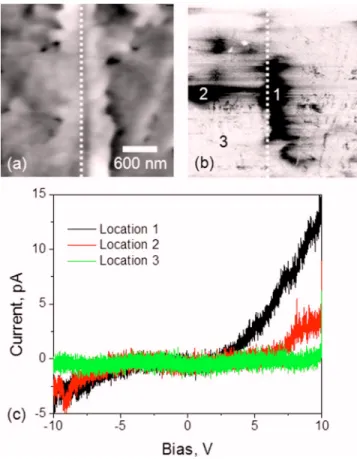
To complement PFM studies and develop insight into the pinning mechanism, transport properties of the interface were probed by conductive AFM, as shown in Figs.3共a兲and 3共b兲. The film and GB region are shown to have a number of conductive locations, presumably associated with dislocations.15Note the increased conductivity along most of the length of the GB. Corresponding current-voltage curves measured at and near the GB are presented in Fig. 3共c兲, il-lustrating early onset of conductivity 共at ⬃3 to 4 V兲 at the GB. At biases required for polarization switching, the GB is essentially conductive, suggesting that minimization of the depolarization energy for a domain wall pinned at the GB may contribute significantly to the pinning mechanism.
To summarize, domain wall motion on a well-defined 24° tilt GB in a BFO 共001兲 bicrystal is studied using the
FIG. 1. 共Color online兲 共a兲 Topography and 共b兲 schematic of GB cross sec-tion. Red and blue lines in共b兲 represent the piezoresponse signal. 关共c兲 and 共d兲兴 PFM amplitude and phase images, respectively, of a region switched uniformly with positive tip bias and backswitched with an increasing nega-tive bias.关共e兲 and 共f兲兴 PFM amplitude and phase images, respectively, of a region switched with a negative bias and backswitched with an increasing positive bias. Scales are共a兲 30 nm, 关共c兲 and 共e兲兴 3 mV, and 关共d兲 and 共f兲兴 360°. The dashed white lines indicate the location of the GB. In关共d兲 and 共f兲兴, bright共dark兲 contrast corresponds to an out-of-plane polarization compo-nent, which points toward共away from兲 the substrate.
FIG. 2.共a兲 Topography and 关共b兲 and 共c兲兴 PFM amplitude and phase images, respectively, of a region switched with a negative bias and backswitched in several locations by positive dc-bias pulses.关共d兲–共f兲兴 PFM phase images following the application of additional dc-bias pulses. Scales are共a兲 10 nm, 共b兲 3 mV, 关共c兲–共f兲兴 360°. Images 共c兲–共f兲 are compensated for a phase offset. The dashed white lines indicate the location of the GB. White “x” marks in 关共d兲–共f兲兴 indicate the location of the tip during the application of additional bias pulses.
FIG. 3. 共Color online兲 共a兲 Topography, 共b兲 current image, and 共c兲 selected current-voltage curves. Scale for共b兲 is ⬃15 pA. The dashed white line in 共a兲 indicates the location of the GB. The dark contrast in 共b兲 is indicative of increased leakage.
142901-2 Rodriguez et al. Appl. Phys. Lett. 93, 142901共2008兲
This article is copyrighted as indicated in the article. Reuse of AIP content is subject to the terms at: http://scitation.aip.org/termsconditions. Downloaded to IP: 140.113.38.11 On: Wed, 30 Apr 2014 22:52:34
combination of PFM, domain writing experiments, and con-ductive AFM. The comparison of PFM amplitudes on posi-tively and negaposi-tively polarized GB regions indicates the presence of a region with a frozen positive polarization com-ponent. The GB is shown to attract a domain wall and act as a pinning center. The symmetry of the pinning behavior with respect to wall polarity suggests the pinning is unrelated to the frozen polarization component. The high conductivity of the GB at biases below those required for wall motion sug-gests the GB conductivity can contribute to domain wall pin-ning by reducing the effective potential acting on the wall and also minimizing the depolarization energy for a domain wall pinned at the interface.
Research was sponsored by the Center for Nanophase Materials Sciences, Oak Ridge National Laboratory, man-aged and operated by UT-Battelle, LLC for the Office of Basic Energy Sciences, U.S. Department of Energy 共B.J.R., S.V.K.兲 and the Director, Office of Science, Office of Basic Energy Sciences, Division of Materials Sciences and Engi-neering, and U.S. Department of Energy under Contract No. DE-AC02-05CH11231 共Y.H.C., R.R.兲. Brian Rodriguez ac-knowledges the financial support of the Alexander von Hum-boldt Foundation. Y.H.C. would also like to acknowledge the support of the National Science Council, R.O.C., under Con-tract No. NSC 97-3114-M-009-001.
1J. F. Scott, Ferroelectric Memories共Springer, Berlin, 2000兲.
2Nanoelectronics and Information Technology, edited by R. Waser共Wiley, Weinheim, Germany, 2003兲.
3A. Gruverman and A. Kholkin,Rep. Prog. Phys. 69, 2443共2006兲. 4P. Paruch, T. Giamarchi, and J.-M. Triscone,Phys. Rev. Lett. 94, 197601
共2005兲.
5G. Catalan, H. Béa, S. Fusil, M. Bibes, P. Paruch, A. Barthélémy, and J. F. Scott,Phys. Rev. Lett. 100, 027602共2008兲.
6A. Gruverman, O. Auciello, and H. Tokumoto,Annu. Rev. Mater. Sci. 28, 101共1998兲.
7C. S. Ganpule, V. Nagarajan, H. Li, A. S. Ogale, D. E. Steinhauer, S. Aggarwal, E. Williams, R. Ramesh, and P. De Wolf,Appl. Phys. Lett. 77, 292共2000兲.
8A. Gruverman, C. Isobe, and M. Tanaka, MRS Symposia Proceedings No.
655共Materials Research Society, Pittsburgh, 2001兲, p. CC8.5.
9Y. H. Chu, M. P. Cruz, C. H. Yang, L. W. Martin, P. L. Yang, J. X. Zhang, K. Lee, P. Yu, L. Q. Chen, and R. Ramesh,Adv. Mater.共Weinheim, Ger.兲
19, 2662共2007兲.
10B. J. Rodriguez, S. Jesse, M. Alexe, and S. V. Kalinin,Adv. Mater.
共Wein-heim, Ger.兲 20, 109共2008兲.
11B. J. Rodriguez, R. J. Nemanich, A. Kingon, A. Gruverman, S. V. Kalinin, K. Terabe, X. Y. Liu, and K. Kitamura, Appl. Phys. Lett. 86, 012906 共2005兲.
12D. F. Xue, S. X. Wu, Y. C. Zhu, K. Terabe, K. Kitamura, and J. Wang,
Chem. Phys. Lett. 377, 475共2003兲.
13A. Agronin, Y. Rosenwaks, and G. Rosenman, Appl. Phys. Lett. 88, 072911共2006兲.
14Y. Kan, X. Lu, H. Bo, F. Huang, X. Wu, and J. Zhu,Appl. Phys. Lett. 91, 132902共2007兲.
15K. Szot, W. Speier, G. Bihlmayer, and R. Waser, Nat. Mater. 5, 312 共2006兲.
142901-3 Rodriguez et al. Appl. Phys. Lett. 93, 142901共2008兲
This article is copyrighted as indicated in the article. Reuse of AIP content is subject to the terms at: http://scitation.aip.org/termsconditions. Downloaded to IP: 140.113.38.11 On: Wed, 30 Apr 2014 22:52:34