Investigation and Effects of Wafer Bow in 3D Integration
Bonding Schemes
K.N. CHEN,1,5Y. ZHU,2 W.W. WU,3,6and R. REIF4
1.—Department of Electronics Engineering, National Chiao Tung University, Hsinchu, Taiwan. 2.—IBM T.J. Watson Research Center, Yorktown Heights, NY 10598, USA. 3.—Department of Materials Science and Engineering, National Chiao Tung University, Hsinchu, Taiwan. 4.—Department of Electrical Engineering and Computer Science, Massachusetts Institute of Technology, Cambridge, MA 02139, USA. 5.—e-mail: [email protected]. 6.—e-mail: [email protected]
This paper investigates and reviews the effects of wafer bow in three-dimensional (3D) integration bonding schemes, including copper wafer bond-ing and oxide fusion wafer bondbond-ing with silicon on insulator (SOI)-based layer transfer technology. Wafer bow criteria for good bonding quality and fabri-cation techniques to minimize wafer bow are introduced for 3D integration technology and applications.
Key words: Wafer bow, wafer bonding, 3D integration
INTRODUCTION
Research on the behavior of thin films on sub-strates has been widely investigated because of their applications in microelectronics.1–8 Some of these studies on thin films used substrate curvature methods,2–4,6which correspond to the measurement of wafer bow. Wafer bow is obtained from the mea-surement of the overall magnitude of wafer curva-ture, and usually refers to the height deviation between the center and the edge of a wafer. Wafer bow may result from the device fabrication process or thin film/device stress on the wafer substrate. Since wafer bonding relies on the surface flatness of the two wafers,9wafer bow may play an important role in stacking or bonding quality.
In addition, wafer-bonding technology, including copper (Cu) and oxide wafer bonding, has been widely applied in 3D integration application.10 Wafer bonding has attracted the attention of many researchers.11–13 Some studies have investigated the materials properties of the bonded layer.11,13 The relationship between bonding temperature and bonding quality has been investigated as well.12 However, there is no report about the effect of wafer bow on wafer-bonding quality and methods to
minimize wafer bow. Understanding the effect of wafer bow is also helpful to accurately study other bonding parameters. This paper reports the effect of wafer bow on Cu bonding quality under different bonding temperatures. In addition, wafer bow evo-lution during SOI-based device fabrication for oxide fusion bonding is reviewed. A process technique, post bow compensation, is reviewed and introduced for wafer bow minimization. Finally, suggestions to minimize effects of wafer bow during the bonding process are proposed for 3D integration.
WAFER BOW IN Cu WAFER-BONDING SCHEME
Experimental Procedures
Wafer bows of unprocessed bare 4-inch (100) prime silicon wafers within the range between 20 lm and 20 lm were investigated in this study. Wafer bows of each silicon wafer before and after depositing 50 nm tantalum (Ta) and 300 nm Cu by electron-beam deposition were measured using a KLA-Tencor thin-film stress measurement. Wafer bow of unprocessed wafers before metal thin-film deposition will be referred to as ‘‘initial wafer bow’’ in the following discussion for convenience.
Two wafers with similar initial wafer bows were chosen as the bonding pair. After Ta and Cu depo-sition, these two wafers were bonded face to face
(Received February 21, 2010; accepted July 29, 2010; published online September 4, 2010)
Ó2010 TMS
using an Electronic Vision EV 450 aligner and AB1-PV under pressure of 4000 mbar for 30 min at a 200°C, 300°C, and 400°C in ambient of 10 3Torr. A DAD-2H/6T automatic dicing saw was used to cut bonded wafers into 5 mm 9 5 mm square pieces at a speed of 0.69 mm/s. After the bonded wafer is sawn into pieces, one bonded piece may stay bonded or separate due to the force applied during sawing. The latter case is denoted here as ‘‘dicing failure.’’ This approach allows us to characterize bonding quality for different initial wafer bows.
To simulate the in situ wafer bow at the bonding temperature, some wafers with different initial wafer bows were subjected to thermal heating from room temperature to 400°C at a ramp rate of 0.4°C/s to measure the evolution of wafer bow. The surface of the Cu film during heating and measurement was capped to avoid oxidation. The ramp rate is similar to the heating rate of the bonding process. In each case, in situ wafer bow measurements were taken at 10°C intervals to monitor the change of wafer curvature.
Results of Wafer Bow Measurements and Dicing Analysis
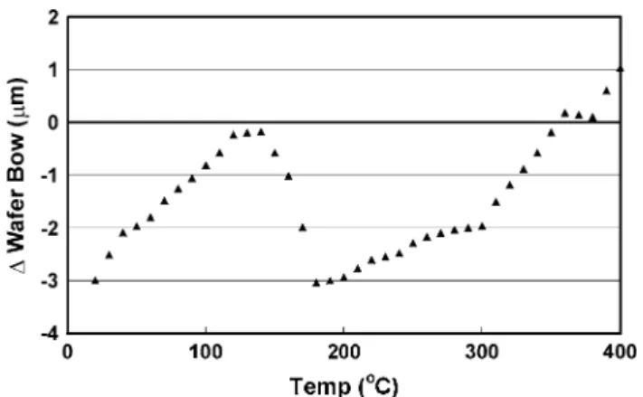
Figure1 shows an example of wafer bow evolu-tion during the heating process from room temper-ature to 400°C. The Y-axis represents the change of wafer bow at each step of measurement relative to the initial wafer bow, which is set at zero. Immedi-ately after depositing Ta and Cu films, the change of wafer bow is 3 lm due to the difference of thermal expansion coefficient between Si and the metals. For other wafers with the same deposition conditions, the change of wafer bow immediately after deposi-tion usually varies from 2 lm to 5 lm. Then the change in the wafer bow becomes less negative during the heating process. However, a more nega-tive change in the wafer bow is observed from 150°C to 200°C. This is because of the microstructure evolution, which includes grain growth of the Cu film.5,8,14 Afterwards, the change of wafer bow
becomes less negative again with increasing tem-perature until it reaches zero and then becomes positive.
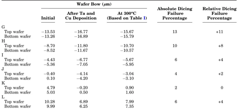
TableI lists the average values of wafer bow change at different temperatures relative to the wafer bow after the deposition of the Ta and Cu films; these are average values of measurements from different wafers. The reason for using the wafer bow after metal film deposition as the refer-ence point is that the initial wafer bow varies from wafer to wafer. By applying the information in the table, it is possible to estimate the wafer bow value at the bonding temperature and to understand the relation between wafer bow, bonding temperature, and bonding quality.
Bonding quality mostly depends on the wafer bow at the bonding temperature, but not on the initial wafer bow. TableIIshows an example of six pairs of wafers selected to be bonded at 300°C. Each pair includes one top wafer and one bottom wafer. Wafer bows of each silicon wafer before and after metal film deposition were measured. The possible wafer bows at 300°C were also estimated based on the information in TableI. To show the effect of wafer bow on bonding quality clearly, in addition to the absolute values of failure pieces during dicing, the relative values are shown. The value of the lowest dicing failure percentage of the bonded wafer is set as zero. The bonded wafer with the lowest dicing failure percentage can be treated as the strongest bonded wafer in the group. For other wafers, the values of dicing failure percentage are the differ-ences from this lowest dicing failure percentage. By using the method, it is easy to determine the strongest bonded wafer and understand the effects of wafer bow on bond strength.
Discussion
In TableII, the dicing failure percentage increases with increasing bow of the wafers to be bonded, for both larger positive and negative values. Pair K showed the strongest wafer-bonding quality. How-ever, it should be noted that pair K did not have the flattest initial wafer bows. In addition, for pair J, with the lowest initial wafer bows, a 2% increase of dicing failure was observed. Therefore, it is sug-gested that the factor that determines bonding quality is the wafer bow at the bonding temperature and not the initial wafer bow.
Fig. 1. An example of wafer bow evolution during the heating pro-cess from room temperature to 400°C. ‘‘D Wafer Bow’’ indicates the difference of wafer bow relative to the initial wafer bow.
Table I. Average change of wafer bow at different temperatures relative to the wafer bow after Ta and Cu film deposition
200°C 300°C 400°C Average change of wafer
bow from room temperature to heating temperature
Figure2 shows the relationship between wafer bow and bonding quality for different bonding tem-peratures. Pairs of wafers with similar initial bows at the desired bonding temperature were bonded. These wafer bows at the bonding temperature were determined from the initial wafer bows and the corresponding wafer bow changes in TableI. Since the wafers of each pair have similar wafer bows, average values of two wafer bows from each wafer pair are used in the figure. It is clear that larger wafer bows result in higher relative dicing failure percentages. When bows of wafers to be bonded increase in magnitude, either positively or nega-tively, the dicing failure percentage increases. Bonded wafer pairs with lower initial wafer bows
have lower failure percentages. Generally speaking, the effect of wafer bow is not obvious when the wafer bow at 200°C, 300°C and 400°C is smaller than ±5 lm, ±8 lm, and ±10 lm, respectively.
Larger wafer bow results in greater local separa-tion between the two surfaces at the beginning of bonding. Although the bonding pressure and the interdiffusion process during bonding can decrease and eliminate a small separation between the two surfaces, there are still some areas that are not close enough and therefore cannot be bonded well when this separation is large. This also explains why the failure percentage does not change much when the wafer bow is small, but increases dramatically when the wafer bow is large.
The effect of wafer bow on bonding quality decreases with increasing bonding temperature. The increase of the dicing failure percentage only reaches 11% when the wafer bows at 300°C are more negative than 15 lm, while with similar wafer bow at 200°C it can reach 19%. In addition, the increase in the relative dicing failure percentage only reaches 8% when the wafer bows are more negative than 15 lm at 400°C. At higher bonding temperature, the greater thermal energy during bonding strengthens the diffusion process within the bonded layer, and the bonding quality is further improved. Therefore, the effect of wafer bow can be balanced by higher bonding temperature to improve bonding quality.
In addition, the failure regions of bonded wafers with positive bows are always located at the edge area, while those with negative bows are located at the center of the wafers. Figure3shows a schematic diagram of these two different failure mechanisms.
Fig. 2. Relation between wafer bow and bonding quality at different bonding temperatures; average wafer bow is the average wafer bow of the two wafers to be bonded.
Table II. Relative dicing failure percentages of wafers with different initial bows when bonded at 300°C Wafer Bow (lm) Absolute Dicing Failure Percentage Relative Dicing Failure Percentage Initial After Ta and Cu Deposition At 300°C (Based on TableI) G Top wafer 13.53 16.77 15.67 13 +11 Bottom wafer 13.26 16.89 15.79 H Top wafer 8.70 11.80 10.70 10 +8 Bottom wafer 8.52 11.67 10.57 I Top wafer 4.43 6.77 5.67 6 +4 Bottom wafer 5.36 7.05 5.95 J Top wafer 0.40 4.14 3.04 4 +2 Bottom wafer 0.10 4.20 3.10 K Top wafer 4.79 0.20 0.90 2 0 Bottom wafer 5.03 0.50 1.60 L Top wafer 10.28 6.89 7.99 6 +4 Bottom wafer 9.99 6.25 7.35
Since the bonding force is applied by using a small pin of the bonder to press the center of the upper wafer, the bonding procedure can be treated as if the upper wafer were pressed at the center by a single-point force, as shown in Fig.3a. In Fig.3b, when the force is applied to the upper wafer at the bonding temperature, the first contact point of positively bowed wafers is the center area, while the first contact point of negatively bowed wafers is the edge area. The bonding process, including inter-diffusion across the interface and grain growth, completes first in the first contact region. Then, the bonded area propagates into neighboring areas until the whole wafer is bonded during the bonding process, as shown in Fig.3c. However, the total bonding area across the wafer depends on the thermal energy, determined by the bonding tem-perature and duration, applied by the system. In addition, the initial wafer bow determines the force required to bring the two curved surfaces together for bonding. Therefore, for limited bonding dura-tion at low bonding temperature, two bowed wafers may not be able to bond across the whole wafer, as shown in Fig.3d. The remaining unbonded area, which had the largest separation between the two surfaces prior to bonding due to the wafer bows, cannot survive the dicing test. Higher bonding temperature or lower initial wafer bow will gen-erate better bonding quality across the wafer.
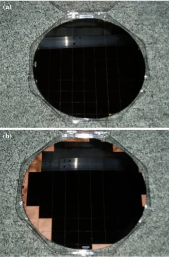
The common approach to determine the quality of wafer bonding qualitatively is the dicing method. During dicing, well-bonded regions stay bonded while poorly bonded regions separate due to the applied stress. The poorly bonded regions occur at the edge of positively bowed wafers and at the cen-ter of negatively bowed wafers (Fig. 3). Figure 4a shows a bonded wafer with a perfect bonding result, while Fig. 4b shows another wafer for which the
edge region failed after bonding.15 In Fig.4b, the two wafers did not bond optimally as both had posi-tive bows before bonding, a result that is consistent with the prediction based on Fig.3.
Material characterizations of unbonded and bonded areas can be carried out by transmission electron microscope (TEM), as shown in Fig.5a and b.16 As shown in Fig.5a, the well-bonded area has perfect bonding quality and no obvious bonding interface can be observed. The poorly bonded region can be observed directly in the TEM image in Fig.5b, and from scanning electron microscope (SEM) and dicing results. The characterization results provide guidelines to determine the bonding parameters for 3D integration.
Since Cu wafer bonding is becoming an attractive choice for future three-dimensional integration,10 the results from this wafer bow investigation offer an important reference for initial wafer selection. To achieve high-quality bonding, the wafer bow should be considered. By applying the criterion of wafer bow described herein, the effect of wafer bow on bonding quality can be effectively avoided.
Fig. 3. Schematic diagram of two failure mechanisms for wafers with different types of wafer bow.
Fig. 4. Images of (a) a well-bonded wafer, and (b) a bonded wafer with poorly bonded regions at the edge after dicing tests.15
WAFER BOW IN OXIDE BONDING BASED ON SOI WAFER SCHEME
Scheme Introduction
In this section, wafer bow effects in the scheme
of oxide bonding based on SOI wafers are
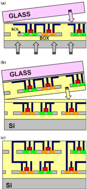
reviewed.15,16 This 3D integration scheme is also known as the ‘‘layer transfer process.’’ A schematic diagram of this scheme is shown in Fig.6.17The top wafer, an SOI wafer, is first attached to a glass handle wafer, followed by removal of the original substrate, as shown in Fig.6a. In Fig. 6b, the top wafer can be aligned and oxide-bonded to the bot-tom wafer. Finally the 3D stacked structure (Fig.6c) can be achieved by releasing the glass handle wafer.17
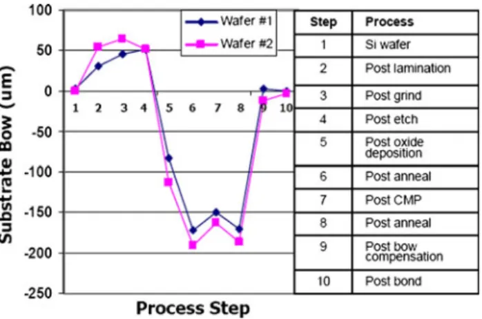
Wafer Bow Evolution in Fabrication Steps It is interesting to know the relation between wafer bow and each wafer fabrication step. Therefore, the evolution of wafer bow was recorded
step by step, as shown in Fig.7.18 Two wafers with almost zero bow were selected for the oxide bond-ing process. The bow became positive (<100 lm) in the first few steps prior to oxide deposition,18 and this value should be adequate to achieve good bonding quality in the subsequent bonding process at this point.
However, once the oxide was deposited, the bow became drastically negative. In step 6, after the postannealing treatment, a huge bow of approxi-mately 200 lm was measured. The bow did not change much after steps 7 and 8.18 This large wafer bow was not acceptable for subsequent oxide bonding.
Fig. 5. Cross-sectional TEM images of (a) a well-bonded Cu inter-face, and (b) a poorly bonded Cu interface at the edge of a bonded wafer.16
Fig. 6. Schematic diagram of 3D integration based on oxide bonding with SOI wafers: (a) the top SOI wafer is attached to a glass handle wafer, followed by removal of the original substrate; (b) the top wafer is aligned and then oxide-bonded to the bottom wafer; (c) the final 3D stacked structure is achieved by releasing the glass handle wafer.17
Wafer Bow Compensation
To overcome this issue, an additional process step, called post bow compensation, was introduced to compensate for the wafer bow.18As shown in step 9 of Fig.7, the bows of both wafers could be mini-mized to around zero again. No obvious wafer deg-radation after oxide bonding was observed with the final bonded wafer bow around zero.18 Post bow compensation can be accomplished by thin-film deposition on the backside of both wafer substrates.
CONCLUSIONS
The effects of wafer bow on bonding quality were investigated. Bonding quality degrades with high wafer bow during bonding, especially at low bonding temperature. The effect of wafer bow on bonding quality at different bonding temperatures was explored. A physical mechanism is discussed to explain the relation between bonding quality and bonding parameters. The wafer bow evolution and bow compensation method of oxide bonding based on SOI wafers are reviewed and discussed. The criterion of wafer bow for good bonding quality and the compensation method can be applied in future device applications.
ACKNOWLEDGEMENTS
This research is supported by the Republic of China National Science Grant Council (Grant No. NSC 98-2218-E-009-013-MY2). The authors acknowl-edge support from National Chiao Tung University, IBM T.J. Watson Research Center, and Massachu-setts Institute of Technology.
REFERENCES
1. P.A. Flinn, D.S. Gardner, and W.D. Nix, IEEE Trans. Electron. Dev. 34, 689 (1987).
2. P.A. Flinn, J. Mater. Res. 6, 1498 (1991).
3. M.D. Thouless, J. Gupta, and J.M.E. Harper, J. Mater. Res. 8, 1845 (1993).
4. J.J. Toomey, S. Hymes, and S.P. Murarka, Appl. Phys. Lett. 66, 2074 (1995).
5. R.P. Vinci, E.M. Zielinski, and J.C. Bravman, Thin Solid Films 262, 142 (1995).
6. R.-M. Keller, S.P. Baker, and E. Artz, J. Mater. Res. 13, 1307 (1998).
7. C.M. Su and M. Wuttig, Appl. Phys. Lett. 63, 3437 (1993). 8. S.P. Baker, A. Kretschmann, and E. Artz, Acta Mater. 49,
2145 (2001).
9. Q.-Y. Tong and U. Gosele, Semiconductor Wafer Bonding: Science and Technology (New York: Wiley, 1999).
10. J.A. Davis, R. Venkatesan, A. Kaloyeros, M. Bylansky, S.J. Souri, K. Banerjee, K.C. Saraswat, A. Rahman, R. Reif, and J.D. Meindl, Proc. IEEE 89, 305 (2001).
11. R. Tadepalli and C. Thompson, Proceedings of the IEEE 2003 International Interconnect Technology Conference (2003), p. 36.
12. K.N. Chen, C.S. Tan, A. Fan, and R. Reif, Electrochem. Solid-State Lett. 7, G14 (2004).
13. F. Shi, H. Chen, and S. MacLaren, Appl. Phys. Lett. 84, 3504 (2004).
14. Y.-L. Shen and U. Ramamurty, J. Appl. Phys. 93, 1806 (2003).
15. K.N. Chen, S.H. Lee, P.S. Andry, C.K. Tsang, A.W. Topol, Y.-M. Lin, J.-Q. Lu, A.M. Young, M. Ieong, and W. Haensch, IEDM Tech. Digest 367 (2006).
16. K.N. Chen, A. Fan, and R. Reif, J. Electron. Mater. 30, 331 (2001).
17. K.W. Guarini, A.T. Topol, M. Ieong, R. Yu, L. Shi, M.R. Newport, and D.J. Frank, IEDM Tech. Digest 943 (2002). 18. A.W. Topol, D.C. La Tulipe, L. Shi, S.M. Alam, D.J. Frank,
S.E. Steen, J. Vichiconti, D. Posillico, M. Cobb, S. Medd, J. Patel, S. Goma, D. DiMilia, M.T. Robson, E. Duch, M. Farinelli, C. Wang, R.A. Conti, D.M. Canaperi, L. Deligianni, A. Kumar, K.T. Kwietniak, C. D’Emic, J. Ott, A.M. Young, K.W. Guarini, and M. Ieong, IEDM Tech. Digest 352 (2005).
Fig. 7. Bow measurement at various fabrication steps in the 3D integration process introduced in Fig.6.18