Embedded indium-tin-oxide nanoelectrodes for efficiency and lifetime enhancement
of polymer-based solar cells
Peichen Yu, Chia-Hua Chang, Ming-Shin Su, Min-Hsiang Hsu, and Kung-Hwa Wei
Citation: Applied Physics Letters 96, 153307 (2010); doi: 10.1063/1.3395395 View online: http://dx.doi.org/10.1063/1.3395395
View Table of Contents: http://scitation.aip.org/content/aip/journal/apl/96/15?ver=pdfcov Published by the AIP Publishing
Articles you may be interested in
Indium tin oxide and indium phosphide heterojunction nanowire array solar cells Appl. Phys. Lett. 103, 243111 (2013); 10.1063/1.4847355
Efficient polymer solar cells with a solution-processed gold chloride as an anode interfacial modifier Appl. Phys. Lett. 102, 163302 (2013); 10.1063/1.4803039
Enhanced performance in polymer solar cells by the use of a halogenated indium tin oxide anode Appl. Phys. Lett. 102, 053302 (2013); 10.1063/1.4790624
Balanced carrier transport in organic solar cells employing embedded indium-tin-oxide nanoelectrodes Appl. Phys. Lett. 98, 073308 (2011); 10.1063/1.3556565
Use of fluorine-doped tin oxide instead of indium tin oxide in highly efficient air-fabricated inverted polymer solar cells
Appl. Phys. Lett. 96, 133506 (2010); 10.1063/1.3374406
This article is copyrighted as indicated in the article. Reuse of AIP content is subject to the terms at: http://scitation.aip.org/termsconditions. Downloaded to IP: 140.113.38.11 On: Wed, 30 Apr 2014 10:27:56
Embedded indium-tin-oxide nanoelectrodes for efficiency and lifetime
enhancement of polymer-based solar cells
Peichen Yu,1,a兲Chia-Hua Chang,1Ming-Shin Su,2Min-Hsiang Hsu,1and Kung-Hwa Wei2,b兲
1Department of Photonics, Institute of Electro-Optical Engineering, National Chiao Tung University, Hsinchu 30010, Taiwan
2Department of Material Science and Engineering, National Chiao Tung University, Hsinchu 30010, Taiwan
共Received 26 January 2010; accepted 23 March 2010; published online 16 April 2010兲
In this paper, distinctive indium-tin-oxide 共ITO兲 nanorods are employed to serve as buried electrodes for polymer-based solar cells. The embedded nanoelectrodes allow three-dimensional conducting pathways for low-mobility holes, offering a highly scaffolded cell architecture in addition to bulk heterojunctions. As a result, the power conversion efficiency of a polymer cell with ITO nanoelectrodes is increased to about 3.4% and 4.4% under one-sun and five-sun illumination conditions, respectively, representing an enhancement factor of up to⬃10% and 36% compared to a conventional counterpart. Also, the corresponding device lifetime is prolonged twice as much to about 110 min under five-sun illumination. © 2010 American Institute of Physics.
关doi:10.1063/1.3395395兴
Worldwide awareness of petroleum scarcity and global climate changes has promoted an increasing demand for clean and renewable energy sources, pushing forward the realization of third-generation solar cells.1Assisted by sim-plistic and scalable fabrication processes, organic solar cells have recently emerged as a competitive alternative to their silicon thin-film counterparts. In particular, the power con-version efficiency 共PCE兲 of polymer-based solar cells has recently exceeded 5% due to the introduction of bulk heterojunctions 共BHJs兲.2–5 However, due to the disordered nature of BHJs, carrier transport remains an issue that limits the PCE from reaching the predicted value of 10%.6–8 Although recent advances in nanofabrication technologies have allowed the formation of ordered BHJs, offering bicon-tinuous, interdigitated networks for carrier transport,9–11the nanoscale templates still result in limited PCEs, possibly due to insufficient infiltration of polymers or twisted polymer chains that may affect the carrier mobility.12,13Here, we in-troduce an alternative cell architecture which alleviates the transport issue by using embedded indium tin oxide 共ITO兲 nanoelectrodes in polymer-based solar cells. In this architecture, the distributed nanorod electrodes are vertically aligned and protruded into the active layers, offering three-dimensional 共3D兲 conducting pathways for low-mobility holes. Conductive atomic force microscopy 共AFM兲 analyses have shown that the current conduction is significantly im-proved with nanorod electrodes. As a result, the PCE of a cell with ITO nanoelectrodes is increased to about 3.4% and 4.4% under one-sun 共1⫻兲 and five-sun 共5⫻兲 illumination conditions, respectively, representing an enhancement factor of up to ⬃10% and 36% compared to a conventional coun-terpart. Also, the corresponding device lifetime, as measured by the degradation time to 80% of the normalized efficiency, is increased twofold to about 110 min under five-sun illumi-nation. The significant efficiency and lifetime enhancements result from the much improved carrier collection probability under high carrier concentrations, suggesting the soundness
of the approach toward improving the survivability of polymer-based solar cells.
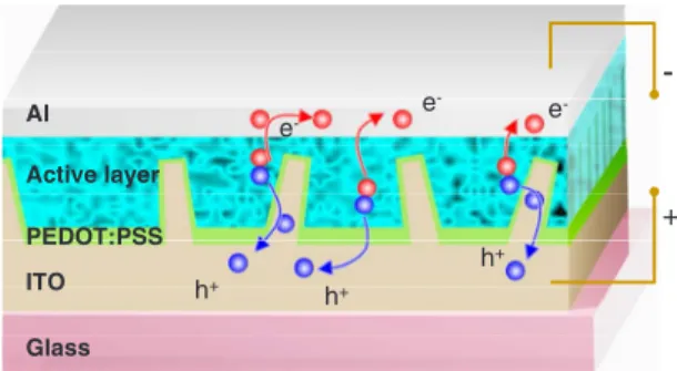
Although the concept of buried electrodes has previously been proposed to increase cell thickness for optical absorp-tion without compromising charge carrier collecabsorp-tion, poly-mer solar cells with submicroscale lamellar electrodes are still rather inefficient due to the lack of suitable electrode materials and challenging fabrication procedures.14 In this work, we demonstrate a deposition technique to form free-standing ITO nanorods which is compatible with the stan-dard fabrication process of polymer cells. Figure1shows the schematic of a fabricated device with embedded nanoelec-trodes. In this cell structure, the randomly oriented nanorod electrodes were deposited on an ITO-coated glass substrate using an oblique electron-beam evaporation method.15,16 A hole transport layer of poly 共3,4-ethylenedioxythiophene兲-polystyrene sulfonate 共PEDOT:PSS兲 was then spin-cast onto the ITO electrodes as the anode. The active region consisted of a mixture of regioregular poly共3-hexylthiophene兲 共P3HT兲 and 关6,6兴-phenyl-C60-butyric acid methyl ester 共PCBM兲 with a weight ratio of 1:1. The device was then annealed at 120 ° C for 30 min, followed by the thermal evaporation of a 100 nm thick Al electrode. The resulting active-layer thick-nesses were ⬃150–200 nm. A conventional P3HT/PCBM cell with an ITO film electrode was also fabricated with the same process conditions for reference.
a兲Electronic mail: [email protected]. b兲Electronic mail: [email protected].
Al Glass ITO Active layer PEDOT:PSS h+ h+ h+ e- e -e -+
-FIG. 1. 共Color online兲 Device schematic with embedded nanoelectrodes. The randomly oriented nanorod electrodes were deposited on an ITO-coated glass substrate using an oblique electron-beam evaporation method, offering 3D conducting pathways for low-mobility holes.
APPLIED PHYSICS LETTERS 96, 153307共2010兲
0003-6951/2010/96共15兲/153307/3/$30.00 96, 153307-1 © 2010 American Institute of Physics
This article is copyrighted as indicated in the article. Reuse of AIP content is subject to the terms at: http://scitation.aip.org/termsconditions. Downloaded to IP: 140.113.38.11 On: Wed, 30 Apr 2014 10:27:56
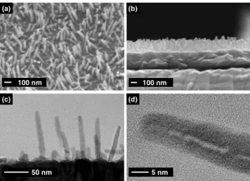
The oblique electron-beam evaporation technique has been used to prepare microscale and nanoscale porous mate-rials based on nucleation formation and self-shadowing effects.17–19Although various techniques have been proposed to grow ITO nanostructures, few have actually resulted in free-standing nanorods with high-aspect ratios.20–22 In this work, a small nitrogen flow rate is introduced to facilitate the segregation of tin-doped indium during nucleation, which promotes the resulting column growth in an oxygen-deficient environment. The scanning electron micrographs共SEMs兲 for a tilted top view and the cross-sectional view of deposited nanorods are shown in Figs.2共a兲and2共b兲, respectively. The deposited nanorods are randomly oriented with heights of ⬃100 to 150 nm and thicknesses of ⬃15 to 30 nm. The density can vary from 5⫻109 to 2⫻1010 cm−2, depending on the deposition rate and temperature. These nanorods can be grown in a single-step deposition, up to an area of 3 ⫻3 cm2. As seen in Fig.2共c兲, the transmission electron mi-croscopic 共TEM兲 image indicates that the spacing between rods is on the order of tens of nanometers, which is sufficient for the infiltration of the spin-cast active materials. The TEM image of a single rod, shown in Fig. 2共d兲, further reveals a composition variation in the transverse direction. Our previ-ous work has confirmed the core-shell structure observed in a relatively thick ITO nanorod, where the structure of the outer shell is relatively amorphous due to a higher tin content than that in the core region. The structure in Fig.2共d兲suggests the initial stage of crystallization toward the rod center. The growth mechanism presumably involves self-catalyst, vapor-liquid-solid phase transitions assisted by the introduced ni-trogen. As opposed to conventional growths of ITO in an oxygen-rich environment, nitrogen facilitates the segregation of tin-doped indium during nucleation due to oxygen defi-ciency. The increased tin content then lowers the melting point of tin-doped indium. As a result, when the substrate temperature becomes higher than the melting point of tin-doped indium, the liquid-phase nucleation cores have a large accommodation coefficient to promote the absorption of indium-oxide and tin-oxide vapors via surface diffusion. This process can lead to high growth rates in specific directions, resulting in randomly oriented nanorods.
The optical transmittance spectroscopy of ITO nanorods deposited on an ITO glass substrate shows a 10–20 nm wavelength shift in the peak transmittance without degrada-tion in magnitudes compared to that of an ITO glass substrate.23The contribution to the enhanced optical absorp-tion due to slight differences in the transmittance spectrum is therefore negligible. Since cell characteristics may be prima-rily determined by electrically-related effects, conductive AFM is employed to study the nanoscale topology and the corresponding current distribution. The measured height im-age and projected current distribution of an ITO glass sub-strate scanned within an area of 1⫻1 m2are shown in Fig. 3共a兲. In Fig.3共b兲, the two-dimensional共2D兲 topology is over-laid with a map of iso-current contours at a threshold of 34.1 nA. The results for the deposited nanorods on an ITO glass substrate are shown in Figs.3共c兲and3共d兲, where the maxi-mum conduction current is as high as 113.7 nA. Since the area scan is performed at a fixed voltage of 10 mV for both samples, the dense and uniformly distributed current spots shown in Fig. 3共d兲 confirm a conductivity improvement with nanorod electrodes. Moreover, the current distribution is particularly concentrated around the nanorod tips, suggest-ing a relatively high carrier collection probability near the tips. Such embedded electrodes allow distributed conduct-ing pathways for low-mobility holes, offerconduct-ing a highly-scaffolded cell architecture, in addition to BHJs, for organic photovoltaic devices. The inhomogeneous drift-field distribu-tion in this device may arguably contribute to the germinate separation compared to conventional BHJ cells, which re-quires further investigation.
Solar cells with embedded ITO nanoelectrodes were characterized under ambient conditions with standard illumi-nation intensities of air mass 1.5, 100 mW cm−2 共one-sun, 1⫻兲 and 500 mW cm−2 共five-sun, 5⫻兲, and also compared to conventional cells fabricated with the same process con-ditions. Hereafter, we refer to the cell with nanorod
elec-100 nm 50 nm 50 nm 5 nm5 nm 100 nm (c) (b) (a) (d)
FIG. 2. SEMs and transmission electron micrographs of deposited ITO na-norods on an ITO glass substrate.共a兲 tilted top view, and 共b兲 cross-sectional view of free-standing nanorods, where the orientations are fairly random;共c兲 the spacing between rods is on the order of tens of nanometers, sufficient for the infiltration of active materials and共d兲 the initial formation of a core-shell structure for a single ITO nanorod.
0 . 0 0 . 2 0 . 4 0 . 6 0 . 8 1 . 0 0 . 0 0 . 2 0 . 4 0 . 6 0 . 8 1 . 0 0 . 0 0 . 2 0 . 4 0 . 6 0 . 8 1 . 0 0 . 0 0 . 2 0 . 4 0 . 6 0 . 8 1 . 0 0 . 0 0 . 2 0 . 4 0 . 6 0 . 8 1 . 0 0 . 0 0 . 2 0 . 4 0 . 6 0 . 8 1 . 0 0 . 0 0 . 2 0 . 4 0 . 6 0 . 8 1 . 0 0 . 0 0 . 2 0 . 4 0 . 6 0 . 8 1 . 0 0 1 0 2 0 3 0 4 0 5 0 6 0 0 1 0 2 0 3 0 4 0 5 0 6 0 0 1 0 2 0 3 0 4 0 5 0 6 0 0 1 0 2 0 3 0 4 0 5 0 6 0 (nm) (nm) 1 µm 1 µm 1 µm 1 µm (a) (b) (c) (d)
FIG. 3. 共Color online兲 Surface topology and the corresponding current dis-tribution for an ITO film and nanorod electrodes.共a兲 The measured height image and projected current distribution of an ITO film electrode on a glass substrate; 共b兲 the corresponding 2D topology overlaid with the map of isocurrent contours at a threshold of 34.1 nA;共c兲 and 共d兲 are the same as 共a兲 and共b兲, respectively.
153307-2 Yu et al. Appl. Phys. Lett. 96, 153307共2010兲
This article is copyrighted as indicated in the article. Reuse of AIP content is subject to the terms at: http://scitation.aip.org/termsconditions. Downloaded to IP: 140.113.38.11 On: Wed, 30 Apr 2014 10:27:56
trodes as the rod cell, and the one with an ITO film electrode as the film cell. The measured current density-voltage 共J-V兲 characteristics are plotted in Fig. 4共a兲for one-sun and five-sun conditions with the corresponding cell characteristics summarized in Table I. The series and shunt resistance are calculated as the inverse slopes at the open-circuit and short-circuit operation points, respectively.24As shown in TableI, the one-sun photocurrent of the rod cell increases by⬃14%, compared to that of the film cell. Since the transmittance and cell thickness does not change significantly with the use of embedded electrodes and the series resistance decreases by ⬃38%, the enhancement of photocurrent and the reduced series resistance are attributed to the improved carrier collec-tion probability using embedded nanoelectrodes. The fill-factor 共FF兲 of the rod cell deteriorates a bit due to a slight degradation of the shunt resistance, possibly originating from a few nanoelectrodes in near contact with the Al cathode. Although not revealed in the preliminary x-ray diffraction analysis, the phase separation of P3HT/PCBM blends may also be affected by nanorod surfaces, which could deteriorate the series and shunt resistance. Overall, the PCE of the rod cell is still enhanced by nearly 10% at one-sun illumination. However, the PCE enhancement becomes prominent with the increased illumination intensity, up to a factor of 36% for the rod cell at a 5⫻ concentration. Since the PCE of both film and rod cells increases with concentration, the enhancement is partly contributed by improved space-charge-limited con-duction. Since most of the trap states are occupied due to increased carrier densities under high illumination, the mo-bility of free carriers increases. However, such contribution
should be rather minor as the PCE of the film cell merely increases by 4%. Therefore, we are convinced that the em-bedded nanoelectrodes can collect holes much more effi-ciently than the film electrodes under high carrier densities, giving rise to a higher PCE enhancement. Both film and rod cells show decreased FFs due to the increased recombination current under high carrier densities, which are also evidenced by the decreased shunt resistance at a 5⫻ concentration. Fi-nally, the lifetime test was performed for both cells at ambi-ent conditions. As shown in Fig.4共b兲, the degradation time to 80% of the normalized efficiency for the rod cell is pro-longed twice as much to about 110 min, compared to 55 min for the film cell. The enhanced lifetime of the rod cell may be attributed to the fast collection of charge carriers, which alleviates the impact of charge accumulation on the electrode interface.25
The authors thank Professor H. C. Kuo at National Chiao Tung University in Taiwan for technical support and Professor X. Cheng at Texas A&M University, Texas, USA for fruitful discussions. This work is funded by National Sci-ence Council in Taiwan under Grant Nos. 96-2221-E-009-095-MY3 and 97-2120-M-006-009.
1M. A. Green, Third Generation Photovoltaics: Advanced Solar Electricity
Generation共Springer, Berlin, 2003兲.
2J. J. M. Halls, C. A. Walsh, N. C. Greenham, E. A. Marseglia, R. H.
Friend, S. C. Moratti, and A. B. Holmes, Nature共London兲 376, 498 共1995兲.
3W. Ma, C. Yang, X. Gong, K. Lee, and A. J. Heeger,Adv. Funct. Mater.
15, 1617共2005兲.
4M. Reyes-Reyes, K. Kim, J. Dewald, R. López-sandoval, A. Avadhanula,
S. Curran, and D. L. Carroll,Org. Lett. 7, 5749共2005兲.
5J. Y. Kim, S. H. Kim, H. H. Lee, K. Lee, W. Ma, X. Gong, and A. J.
Heeger,Adv. Mater. 18, 572共2006兲.
6K. M. Coakley and M. D. McGehee,Chem. Mater. 16, 4533共2004兲. 7M. C. Scharber, D. Mühlbacher, M. Koppe, P. Denk, C. Waldauf, A. J.
Heeger, and C. J. Brabec,Adv. Mater. 18, 789共2006兲.
8W. Shockley and H. J. Queisser,J. Appl. Phys. 32, 510共1961兲. 9M. Aryal, F. Buyukserin, K. Mielczarek, X. M. Zhao, J. Gao, A. Zakhidov,
and W. Hu,J. Vac. Sci. Technol. B 26, 2562共2008兲.
10C. Goh, K. M. Coakley, and M. D. McGehee,Nano Lett. 5, 1545共2005兲. 11H. S. Wang, L. H. Lin, S. Y. Chen, Y. L. Wang, and K. H. Wei,
Nanotech-nology 20, 075201共2009兲.
12A. C. Mayer, S. R. Scully, B. E. Hardin, M. W. Rowell, and M. D.
McGe-hee,Mater. Today 10, 28共2007兲.
13T. W. Zeng, Y. Y. Lin, H. H. Lo, C. W. Chen, C. H. Chen, S. C. Liou, H.
Y. Huang, and W. F. Su,Nanotechnology 17, 5387共2006兲.
14M. Niggemann, M. Glatthaar, A. Gombert, A. Hinsch, and V. Wittwer, Thin Solid Films 451-452, 619共2004兲.
15P. Yu, C. H. Chang, C. H. Chiu, C. S. Yang, J. C. Yu, H. C. Kuo, S. H.
Hsu, and Y. C. Chang,Adv. Mater. 21, 1618共2009兲.
16C. H. Chang, P. Yu, and C. S. Yang,Appl. Phys. Lett. 94, 051114共2009兲. 17M. M. Hawkeye and M. J. Brett,J. Vac. Sci. Technol. A 25, 1317共2007兲. 18Y. P. Zhao, D. X. Ye, G. C. Wang, and T. M. Lu,Proc. SPIE 5219, 59
共2003兲.
19J. Q. Xi, M. F. Schubert, J. K. Kim, E. F. Schubert, M. Chen, S.-Y. Lin, W.
Liu, and J. A. Smart, Nat. Photonics 1, 176共2007兲.
20H. Yumoto, T. Sako, Y. Gotoh, K. Nishiyama, and T. Kaneko,J. Cryst. Growth 203, 136共1999兲.
21Q. Wan, Z. T. Song, S. L. Feng, and T. H. Wang,Appl. Phys. Lett. 85,
4759共2004兲.
22S. J. Limmer, S. V. Cruz, and G. Z. Cao, Appl. Phys. A: Mater. Sci. Process. 79, 421共2004兲.
23See supplementary material athttp://dx.doi.org/10.1063/1.3395395for the
spectral transmittance.
24M. S. Kim, B. G. Kim, and J. Kim,Appl. Mater. & Interfaces 1, 1264
共2009兲.
25K. Kawano and C. Adachi,Adv. Funct. Mater. 19, 3934共2009兲.
(a)
0.00 0.25 0.50 0.75 -80 -60 -40 -20 0 20 40 Film Cell (1x) Rod Cell (1x) Film Cell (5x) Rod Cell (5x) Curre n t D e n sit y (mA/ cm 2 ) Voltage(V) 0 40 80 120 160 60 70 80 90 100 Rod Cell Film Cell Nor m ali z ed Ef fic iency (%) Time (min.)(b)
FIG. 4. 共Color online兲 Measured current-density-voltage and lifetime char-acteristics for a rod cell and a film cell.共a兲 The power conversion efficiency of the rod cell is increased to about 3.4% and 4.4% under one-sun and five-sun illumination intensities, respectively. 共b兲 The measured lifetime characteristics under a 5⫻ concentration at ambient conditions.
TABLE I. Cell characteristics under one-sun and five-sun illumination in-tensities. Device共suns兲 Jsc 共mA/cm2兲 Voc 共V兲 FF 共%兲 PCE 共%兲 Rs 共⍀ cm2兲 Rsh 共⍀ cm2兲 Film cell共1⫻兲 8.35 0.60 62.13 3.11 10.3 250.0 Rod cell共1⫻兲 9.53 0.61 58.70 3.41 6.4 212.2 Film cell共5⫻兲 48.08 0.66 50.99 3.24 4.5 66.0 Rod cell共5⫻兲 67.88 0.66 49.30 4.41 4.0 49.6
153307-3 Yu et al. Appl. Phys. Lett. 96, 153307共2010兲
This article is copyrighted as indicated in the article. Reuse of AIP content is subject to the terms at: http://scitation.aip.org/termsconditions. Downloaded to IP: 140.113.38.11 On: Wed, 30 Apr 2014 10:27:56