IEEE ELECTRON DEVICE LETTERS, VOL. 17, NO. 5, MAY 1996 199
A Novel Vertical Bottom-Gate Polysilicon Thin
Film Transistor with Self-Aligned Offset
Chao Sung Lai, Chung Len Lee, Tan
Fu Lei, and Horng Nan Chern
Abstract- A novel device structure for the vertical bottom polysilicon gate thin film transistor (TFT) with a self-align offset drain is proposed and demonstrated. The new VTFT allows a deep-submicron channel length, which is determined by the thickness of the active polysilicon film, not by the lithographic system resolution. The self-alignment offset drain reduces the leakage current, as a result, it exhibits good device performance.
I. INTRODUCTION
ERTICAL thin film transistors (VTFT’s) are suitable for
V
high density integration since their channel length are determined by the thicknesses of Si02 or polysilicon~ films instead of the photolithographic limitation. Much work had been devoted to developing and studying VTFT’s [ 1]-[3]. The inverted TFT structure is more advantageously used in an integrated circuit for increasing integration density and improving the topography [4]. For inverted TFT’s which have the gate below the channel, the conventional self-aligned structure cannot be achieved. Another problem for TFT’s is that its leakage current, which is caused by the off-state drain field, is relatively large since it is a short channel device. The leakage current can be reduced by drain engineering such as by adding an offset structure [4]-[6]. However the offset structure needs an additional masking step which makes the fabrication for the device rather complicated and difficult.In this letter, we propose and demonstrate a novel VTFT structure which has the inherent off-set drain structure. The self-aligned feature eliminates the additional photolithographic step and the fabricated device exhibited submicron device characteristics.
11. DEVICE STRUCTURE AND FABRICATION
TABLE I
THE MEASURED VALUES OF THE DEVICE PARAMETERS OF VTFT’S WITH AND WITHOUT THE DRAIN OFFSET BEFORE AND AFTER THEY HYDROGENATED
Control
3.15 6.56 3.20 2.10 sample
at 625OC and doped with POCIS. The film was photolitho- graphically defined to obtain the polysilicon bottom gate. After that, the wafer was loaded into an oxide etcher to etch the isolation oxide to form the offset structure [Fig. l(a)]. The wafer was then deposited with a TEOS oxide and annealed in 0 2 at 850°C for 30 min to form the gate oxide. Another undoped 450
A
amorphous silicon was deposited again by LPCVD to form the active channel of the device. The wafer was annealed at 600°C for 24 h to transform the amorphous silicon into polysilicon. A 300A
pad-oxide was deposited by LPCVD and an Arsenic implantation of a dose of 2 x 10l5/cm2 was performed vertically to form source/drain regions which were activated at 850°C for 1 h in nitrogen. After sourceldrain regions were defined and etched [Fig. l(b)], isolation oxide was deposited and contact holes were opened. Finally, AI was deposited and defined for electrodes.For comparison, a device (control sample) without etching the offset drain structure during the step of isolation oxide etching of Fig. l(a) was also fabricated.
The device structure is illustrated in Fig. l(c) with its fabrication steps in Fig. l(a)-(c). The device has two vertical channels with the source at the top and the offset drains at the two sides of the isolation oxide. The key processing steps are as follows:
A silicon wafer was first oxidized to form 800 nm of isolation oxide. Then a 800 nm polysilicon film was deposited by a low-pressure chemical vapor deposition (LPCVD) system
111. RESULTS AND DISCUSSION
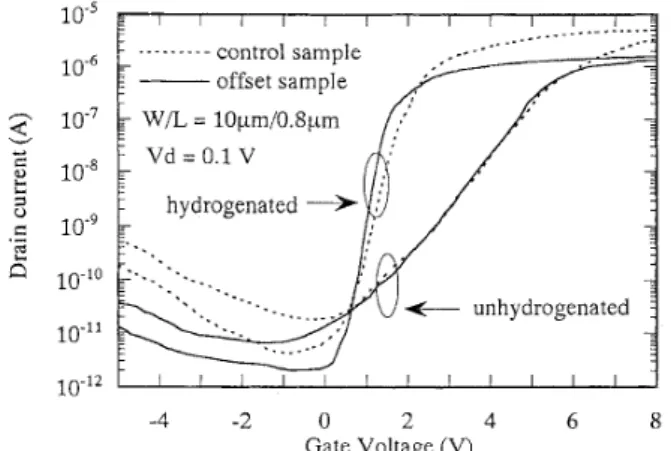
The channel length of this device was determined by the thickness of bottom poly-% gate and the length of the offset region was determined by the etching of the isolation oxide. Fig. 2 shows the I D - ~ G characteristics, UnhYdrogenated and hydrogenated, of this VTFT with a
w k
of 10 d 0 . 8 bm,along with those of the control device. The subthreshold
Manuscript received September 14, 1995; revised January 18, 1996. This work was supported by the National Science Council, ROC, through research contract NSC84-2215-E009-003, and the technical support of National Nano
swings were 0.96 V/decade and 0.24 V/decade for the un- hydrogenated and hydrogenated For
Device Laboratorv. control device, they were 0.99 Vldecade and 0.30 Vldecade,
The authors are with the Department of Electronics Engineering and Institute of Electronics, National Chiao Tung University, Hsingchu, Taiwan, ROC.
respectively. The dynamic ranges of both the offset and control hydrogenated devices were greater than six decades. However, due to the corners of poly-Si gate, the gate oxide will be
Publisher Item Identifier S 0741 -3 106(96)03727-5.
200 IEEE ELECTRON DEVICE LETTERS, VOL. 17, NO. 5 , MAY 1996 I t
offset
etching Isolation Oxide ASIon Imulantation 2x10¹⁵
1
1‘J
1
!
I
I l l Isolation Oxidei
Isolation OxideI
offset
offset
I
Fig. 1. The main fabrication steps and the cross-sectional schematic of the proposed VTFT. (a) 1. Wet-oxidation 800 nm, deposit poly-Si 800 nm and dope. 2. Define bottom poly-Si gate, etch isolation oxide (100 nm) to form onset region. 5 . veposir oxiae as gare aieiecrric. to) 4. veposir a - x ana recrystalize. 5. Deposit pad oxide and ion implant. (c) 6. Deposit passivation oxide. 7. Etch contact hole and A1 metalize.
subjected to high electric field and result in early breakdown of gate oxide.
When an off-set structure is introduced, several changes are observed in Fig. 2. First, compared to the control device, the
_._._-.--- . . . control sample offset sample 10-6 v Y C 2 1 C .I 2
a
10-8 1 0 - 1 0 10-11 1 0 - 1 2 -4 -2 0 2 4 6 8 Gate Voltage (V)Fig. 2 The I D - 1% characteristics at the drain voltage VD = 0.1 V of VTFT’s, unhydrogenated and hydrogenated, with and without the drain offset.
leakage current is effectively reduced as the offset structure is introduced. The leakage current was due to field enhanced carrier emission via trap states near the drain junction [7], [8]. The offset region reduces the electric field at the drain junction, and controls the leakage current. Second, a reduction of the saturation current is observed, as a series resistance is added by the offset region on the drain side.
Table I compiles the subthreshold swing (S), threshold voltage (Vth), mobility, the minimum leakage current ( I m i n )
and leakage current at VG = - 5 V ( I D ) of two devices. The table shows that both devices exhibit submicron characteristics and the offset device had even better characteristics in terms of all the above parameters.
IV. CONCLUSION
This letter reports a novel VTFT structure with a self- aligned offset drain. This VTFT exhibited good characteristics and allows a deep-submicron channel length without the pho- tolithographic system limitation. The source and drain of this bottom gate vertical TFT were self-aligned by ion implantation and the channel length was determined by thicknesses of bottom polysilicon films. The leakage current was reduced by the self-aligned offset drain structure without an additional lithography step.
REFERENCES
[ I ] S. Ikeda, S. Hashiba, I. Kuramoto, H. Katoh, S. Ariga, T. Yamanaka, T. Hashimoto, N. Hashimoto, and S. Meguro, “A polysilicon transistor
for large capacity SRAM’s,” IEDM Tech Dig., p. 469, 1990. [2] T. Zhao, M. Cao, K. C. Saraswat, and J. D. Plummer, “A vertical
submicron polysilicon thin-film transistor using a low temperature process,” IEEE Electron Device Lett., vol. 15, p. 415, 1994. [3] S. D. S. Malhi, P. K. Chatterjee, T. D. Bonifield, J. E. Leiss, D. E. Carter,
R. F. Pinizzotto, and D. J. Coleman, “Edge-defined self-alignment of submicrometer overlaid devices,” IEEE Electron Device Lett., vol. 5, p.
428, 1984.
[4] C. T. Liu, C. H. Douglas Yu, A. K. Kornblit, and K. H. Lee, “In- verted thin-film transistor with a simple self-aligned lightly doped drain structure,” IEEE Truns. Electron Devices, vol. ED-39, no. 12, p. 2803, 1992.
[5] K. Tanaka, H. Arai, and S. Kohda, “Characteristics of offset-structure polycrystalline-silicon thin-film transistors,” IEEE Electron Device Lett.,
LA1 et ul.: NOVEL VERTICAL BOTTOM-GATE POLYSILICON 20 1
[6] S. Seki, 0. Kogure, and B. Tsujiyama, “Laser-recrystalized [8] S. K. Madan and D. A. Antoniadis, “Leakage current mechanisms in hydrogen-passivated fine-grain polycrystalline silicon on insulator MOSFET’s,” ZEEE Trans. Electron Devices, vol. ED-33, no. 10, p. 1518, 1986.
[9] K. Tanaka, H. Arai, and S. Kohda, “Characteristics of offset-structure polycrystalline thin film transistors,” ZEEE Electron Device Lett., vol. 9, p. 23, 1988.
polycrystalline-Silicon thin-film transistors with low leakage current and high switching ratio,” IEEE Electron Device Lett., vol. 8, p. 434, 1987. and A. Chi- ang, “Mechanism and device-to-device variation of leakage current in polysilicon thin film transistors,” IEDM Tech. Dig., p. 867, 1990.