國 立 交 通 大 學
機械工程學系
碩士論文
以電鍍鎳-鑽石奈米複材改進梳狀致動器性能之研究
Performance Enhancement of Comb Drive Actuators Utilizing
Electroplating of Nickel-Diamond Nanocomposite
研 究 生:李毅家
指導教授:鄭裕庭 博士
徐文祥 博士
以電鍍鎳-鑽石奈米複材改進梳狀致動器性能之研究
Performance Enhancement of Comb Drive Actuators Utilizing
Electroplating of Nickel-Diamond Nanocomposite
研 究 生:李毅家 Student:Yi-Chia Lee
指導教授:鄭裕庭 Advisor:Yu-Ting Cheng
徐文祥 Wensyang Hsu
國立交通大學
機械工程學系
碩士論文
A ThesisSubmitted to Department of Mechanical Engineering College of Engineering
National Chiao Tung University In Partial Fulfillment of the Requirements
For the Degree of Master in
Mechanical Engineering June 2005
Hsinchu, Taiwan, Republic of China
以電鍍鎳-鑽石奈米複材改進梳狀致動器性能之研究
學生:李毅家 指導教授:鄭裕庭
徐文祥
國立交通大學機械工程學系 碩士班
摘 要
在微機電的研究領域之中,常以矽作為元件之材料。由材料的觀點出發,矽本身擁 有優良的機械性質;但導電之性質必須藉由摻雜來提升。在製程方面,矽之操作溫度偏 高,導致以其所製作之元件與電路難以整合。反觀金屬本身即具有導電特性;製程上, 可藉由電鍍獲得所需結構,操作溫度接近室溫,此項特性大大提升元件與電路之間的整 合性。 由相關的研究發現,在金屬鎳中添加奈米粉末,可以改變鎳之部分機械性質,例如 在鎳中加入奈米等級的鑽石粒子,可以增加鎳之楊氏係數,根據此結果,將其應用於梳 狀致動器上,使其比純鎳所製作之梳狀致動器擁有更高的共振頻率。 在製程方面,以往電鍍之梳狀致動器容易產生挫曲的結構。在此,調整電鍍參數以 改 變 結 構 之 內 應 力 , 其 中 包 括 電 流 密 度 與 操 作 溫 度 兩 大 重 要 參 數 , 將 其 調 整 至 1.2mA/cm2,35℃即可解決內應力造成之結構挫曲問題。 在量測結果方面,以奈米壓痕器量測純鎳以及鎳-鑽石鍍膜,發現楊氏係數由 173GPa 提升至217GPa。在共振頻率量測方面,針對純鎳與在電鍍液中添加 2g/L 的鑽石奈米粉 末兩種不同材料所製作之梳狀致動器。發現第一模態的頻率由8.034kHz 移至 8.949kHz, 提升了 11.3%,與模擬所得之 10.2%提升量之數值接近,驗證了鑽石奈米粉末可提升電 鍍鎳之梳狀致動器之共振頻率。Performance Enhancement of Comb Drive Utilizing
Electroplating of Nickel-Diamond Nanocomposit
e
Student:Yi-Chia Lee Advisors:Yu-Ting Cheng
Wensyang Hsu
Department of Mechanical Engineering
National Chiao Tung University
Abstract
In MEMS field, most devices are fabricated by silicon. Silicon provides good mechanical properties. The conductivity of silicon must be improved by doping process. The high temperature process of silicon makes MEMS devices difficult to integrate with IC. Comparing with silicon, metal doesn’t need doping process. By electroplating, the problem of high temperature is solved because electroplating is a low temperature process.
In the previous researches, it is found that some kinds of nano particles change some mechanical properties of nickel. For example, diamond nano particles improve the Young’s modulus of nickel. According to this characteristic, the comb drive made by nickel-diamond nanocomposite gets higher resonant frequency than pure nickel one.
The bending of comb drive is the biggest problem of fabrication process. It can be solved by tuning the parameters of electroplating conditions which include current density and operation temperature. Under 1.2mA/cm2 and 35℃, it is possible to get the structure with no bending.
The Young’s modulus is measured by nano indenter. For diamond concentration of 2g/L, the diamond nano particles improve the Young’s modulus of nickel from 173GPa to
217GPa. The resonant frequency is measured by Laser Doppler Vibrometer. The frequency of first mode shifts from 8.034kHz to 8.949kHz. There is an 11.4% improvement. This value is close to 10.2% which is gotten by simulation. It is precisely on such grounds that diamond nanoparticles can improve the resonant frequency of comb drive made by electroplating nickel.
Acknowledgements
I wish to express my gratitude to my advisors, Dr. Yu-Ting Cheng and Dr. Wensyang Hsu, for valuable advice. Also, I would like to thank my colleagues of our group for the helpful suggestions in the past two years. Moreover, I would like to express my appreciations to the Nano Facility Center of National Chiao-Tung University, Dr. Cheng’s group in Department﹙Institute﹚of Electronics Engineering in National Chiao-Tung University, and Chip Implementation Center for providing technical supports and measurement facilities.
Contents
摘 要... i
Abstract ...ii
Acknowledgements ... iv
Contents... v
Figure Captions ...vii
Table Captions... ix
CHAPTER 1 INTRODUCTION... 1
1.1MOTIVATION... 1
1.2RELATED LITERATURE... 2
1.2.1 Comb Drive with Silicon-Based ... 2
1.2.2 Nickel and Nickel Nanocomposite ... 4
1.3CURRENT APPROACH... 6
CHAPTER 2 DESIGN AND ANALYSIS ... 8
2.1DESIGN OF COMB DRIVE... 8
2.2ANALYTIC SOLUTION AND FEMRESULT... 8
2.3MODAL SHAPE DISCUSSION... 11
CHAPTER 3 FABRICATION PROCESS ... 14
3.1FABRICATION PROCESS... 14
3.1.1 Sacrificial Layer... 14
3.1.2 Process Flow... 17
3.3NICKEL AND NICKEL-DIAMOND ELECTROPLATING... 22
3.3.1 Setup of the Electroplating System... 23
3.3.2 Current Density Effect ... 26
3.3.3 Temperature Effect... 28
3.4RESULTS OF ELECTROPLATING... 30
CHAPTER 4 MEASUREMENT AND DISCUSSION ... 33
4.1MATERIAL PROPERTY MEASUREMENT... 33
4.1.1 Measurement of CTE... 33
4.1.2 Measurement of Young’s Modulus and Hardness... 35
4.2RESONANT FREQUENCY MEASUREMENT... 37
CHAPTER 5 CONCLUSION... 42
Figure Captions
Figure 1-1 comb structures with spring beams on each side[1] ... 4
Figure 1-2 (a, left) a partially released nickel microresonator. (b, right) a full released nickel cordierite microresonator[12] . ... 6
Figure 1-3 E/ρ-Diamond concentration [13] . ... 7
Figure 2-1 the model the comb drive by Ansys... 10
Figure 2-2 the (a) first mode; (b) second mode; (c) third mode of comb drive modal simulation. ... 12
Figure 3-1 the structure of the comb drive. ... 14
Figure 3-2 PR sacrificial layer after soft bake (no hard bake)... 15
Figure 3-3 PR sacrificial layer after soft bake (hard bake less)... 16
Figure 3-4 Cu sacrificial layer. ... 16
Figure 3-5 profile of Cu sacrificial layer under different current densities. ... 17
Figure 3-6 process flow chart. ... 19
Figure 3-7 AZ9260 after developed (the original comb gap is 4µm) ... 20
Figure 3-8 AZ9260 after developed by diluting the developer (the original comb gap is 4µm)... 21
Figure 3-9 sidewall of comb drive... 21
Figure 3-10 setup of the electroplating system... 24
Figure 3-11 (a) tank; (b) cathode part; (c) anode part; (d) ventilated system. ... 25
Figure 3-12 the cathode part with sample... 25
Figure 3-13 the electroplating system. ... 26
Figure 3-14 nickel electroplating with high current density (22mA/cm2). ... 27
Figure 3-15 nickel electroplating with low current density (1.2mA/cm2). ... 28
Figure 3-16 current density-deposition rate for nickel electroplating... 28
Figure 3-17 comb drive (a) at room temperature; (b) at 80℃. ... 29
Figure 3-19 (a) full view; (b) spring part; (c) surface of comb drive by nickel-diamond... 31
Figure 3-20(a) full view; (b) spring part; (c) surface of comb drive by nickel-CNT... 32
Figure 4-1 (a) TEM photo of nickel-diamond in Teh’s research[13]; (b) SEM photo of nicke-phosphorus-diamond in Shen’s research[14]. ... 33
Figure 4-2 (a) Young’s modulus and (b) hardness of pure nickel... 36
Figure 4-3 (a) Young’s modulus and (b) hardness of nickel-diamond... 36
Figure 4-4 Frequency-Displacement relation of pure nickel comb drive form 1kHz to 21kHz. ... 39
Figure 4-5 Frequency-Displacement relation of pure nickel comb drive form 7kHz to 10kHz. ... 39
Figure 4-6 Frequency-Displacement relation of nickel diamond comb drive form 3kHz to 22kHz. ... 40
Table Captions
Table 2-1 the critical dimension of comb drive. ... 8
Table 2-2 analytical solution and FEM simulation of the resonant frequency... 10
Table 2-3 the resonant frequencies of pure nickel and nickel-diamond under different mode. ... 13
Table 3-1 the quantities of compositions in the nickel electroplating solution... 23
Table 4-1 the results of CTE measurement... 34
Chapter 1 Introduction
1.1 Motivation
Over the past few years a considerable number of studies have been made on MEMS devices. On the basis of what are needed for MEMS devices, many kinds of fabrication processes which are developed from IC processes have been proposed. MUMPs is a notable example.
Most of these processes utilize silicon as the structure material. With the exception of silicon, metal is interested because of many superior material properties of it in certain applications. First, metal needn’t doping process to improve the conductivity. Secondly, metal process is easier to achieve thick structure. Thirdly, it is easy to obtain metal structure at low temperature. High temperature process always brings the thermal stress issue. Thermal stress causes bending especially for suspended structures.
Nickel is one of the commonest metals applied to MEMS devices and it can be realized by electroplating. There are several articles which have been devoted to this study. Some of them point out that nickel with nanoparticles in it can improve specific properties. For example, nickel with diamond nanoparticles in it has higher Yung’s modulus than pure nickel. It is helpful for nickel applied to RF devices because the higher Young’s modulus improves the higher resonant frequency.
In MEMS application, comb drive is one of the most popular and famous microdevice. It is a good example of RF device which is designed and fabricated by MEMS fabrication processes.
Now using metal as the structural material, the performances of comb drive is decided by what is used as the structure material. Young’s modulus and density are key properties
because they influence the resonant frequency deeply. Device fabricated with high E/ρ ratio material can obtain higher resonant frequency than others. So utilizing nickel-diamond nanocomposite as the structural material, comb drive will be fabricated by electroplating. Resonant frequency improvement of comb drive made by nickel will obtain by test.
1.2 Related Literature
1.2.1 Comb Drive with Silicon-Based
There were many literatures on comb drive. In 1989, comb-drive were reported by Tang et al [1]. The design of comb drive actuators is shown in Figure 1-1. The concept of actuation was using the relation between electrostatic force and spring force. Voltage was the input signal. Different voltage applied on the different combs and resulted in electrostatic force between active and immobile combs. After the balance between electrostatic force and spring force provided form the eight beams suspend on the two side of the active combs part, the output signal displacement was obtained. By matching the frequency of the input signal with the resonant frequency of comb drive structure, large displacement was obtained.
In order to improve the performance of comb drive actuators, many researches were published to show the ways to achieve it. Using comb drive as a resonator, the resonant frequency is the most important point needs to be improved. From the frequency equation, the frequency depends on the spring constant and the mass of the system. The spring constant and the mass of the system can be adjusted by the dimensions and the material of the structure. Actually, searching for the suitable materials is the main destination.
In Tang’s fabrication process, low pressure chemical vapor deposition (LPCVD) polycrystalline silicon was utilized as the structural material [1]. The operation temperature
of LPCVD polycrystalline silicon was above 600 . The high temperature process induced ℃ thermal stress and low deposition rate were the issues of polycrystalline silicon. Biebl et al presented a method to improve the deposition rate, resistivity, and residual stress [2]. By controlling the ratio of phosphine to silane and rapid thermal annealing (RTA) process, the 42 Å/min deposition and 0.8mΩcm resistivity were obtained. A cantilever beam with 2 µm in thickness and 1000µm in length showed an end deflection of less than 0.2µm.
Franke et al used polycrystalline germanium instead of polycrystalline silicon as structural material in 1999 [3]. The fabrication process included LPCVD and RTA. By this process, low resistivity and tensile polycrystalline germanium film was obtained. The testing results showed that RTA process shifted the film stress form tensile to compressive. So by well control of deposition and annealing condition, the film stress could be minimized.
The polycrystalline silicides were bought up as the structural materials. Tri-layer polycrystalline SiGe structure could reduce the strain gradient [4]. Polycrystalline SiC provided high Young’s modulus up to 710 GPa [5]. These two materials both deposited by LPCVD and needed RTA process to reduce thermal stress.
Comb drives were made by surface micromachining in these literatures above. There were some comb drives made by bulk micromachining. The most popular example was using the SOI wafer to achieve it [6][7][8]. The thick silicon layer was utilized as the structure and fabricated by bulk micromachining, so the high aspect ratio combs were obtained. This method was usually used as the vertical driving comb drive because it provided larger area for comb sidewall.
Figure 1-1 comb structures with spring beams on each side[1].
1.2.2 Nickel and Nickel Nanocomposite
Being a new technology, electroplating nickel provides many advantages. High deposition rate, easy stress control, low deposition temperature, and low resistivity are the advantages of electroplating nickel instead of polycrystalline silicon [9][10]. By choosing the suitable fabrication process, it is well suited for post processing on preprocessed CMOS wafers.
In the development of nano particles in metal, based on electroplating nickel, there were some materials being added into the solution of electroplating. In 2002, Teh et al used the ceramic particles as the additive to electroplate the nickel ceramic composite film [11]. Ceramic particles, either in the form of cordierite, or iron oxide, dispersed well within the solution. After fabrication of the nickel ceramic film, the testing result showed that composite film significantly reduced the mismatch of thermal expansion between nickel and silicon. Fortunately, the Young’s modulus, Berkovich hardness, and electrical resistivity were maintained.
After nickel ceramic composite film, Teh et al used diamond and cordierite as the additive [12]. In Figure 1-2, the left microresonator was made by nickel and the right one was made by nickel cordierite. Obviously, the nickel cordierite microresonator was residual stress free because of the better thermal compatibility with silicon. By adding various concentration of diamond particles, it was found that higher diamond concentration obtained the film with more compressively stress.
In 2003, Tsai et al followed Teh’s research and used nickel and diamond nanoparticles as the materials of electro-thermal microactuators [13]. The E/ρratio of microactuators could be enhanced 7.1 times with diamond concentration of 2 g/l. Comparing to device made of electroplated nickel, the microactuators with diamond concentration of 2 g/l could reduce 73% power requirement for 3µm displacement of cantilever beam.
The similar research is taken by Shen in 2004 [13]. The Ni-P-CNT and Ni-P-Diamond films are gotten by electroless. The E/ρ ratios reach 3.9 and 3 times for Ni-P-CNT and Ni-P-Diamond individually. The electrical conductivities are 1.903x10⁻⁶Ω-m and 1.399x10⁻⁶Ω-m.
Comparing metal-based with surface silicon-based micromachining, the deposition rate and thermal stress will be improved. Although using bulk silicon-based micromachining is good for the aspect ratio and the fabrication, it is not easy to integrate comb drive with IC
process and the cost SOI wafer is high. Using metal based process will solve these problems in bulk silicon-based micromachining.
Figure 1-2 (a, left) a partially released nickel microresonator. (b, right) a full released nickel cordierite microresonator[12].
1.3 Current Approach
In previous researches, it is found that nickel-diamond nanocomposite can enhance the E/ρ ratio. As Figure 1-3 indicates, the E/ρ ratio can be enhanced 7.1 times with 2g/L diamond concentration. Basing on this enhancement, comb drive is used as the test device to demonstrate the application of nickel-diamond nanocomposite. The enhancement of the E/ρ ratio promotes the resonant frequency of comb drive.
The deposition method is electroplating. By adding diamond nano particles into the electroplating solution, the nickel-diamond nanocomposite can be deposited. In previous researches, it is sure that diamond nano particles are well dispersed within the nickel film.
In brief, the objective of this thesis is to demonstrate nickel-diamond nanocomposite can be used to fabricate comb drive and the resonant frequency is considered as the performance of comb drive to compare with pure nickel one.
Chapter 2 Design and Analysis
2.1 Design of Comb Drive
The structure of comb drive follows Tang’s design. It is similar to what is shown in Figure 1-1 and the dimensions of comb drive are based on the fabrication ability. So the dimension is decided and the critical dimension of comb drive is shown in Table 2-1.
Table 2-1 the critical dimension of comb drive.
dimension length (µm) width (µm) thickness (µm)
spring 300/250/200 10 7
comb 100 10 7
2.2 Analytic Solution and FEM Result
Comb drive can be considered as the spring-mass damping system and the resonant frequency can be written as the following equation:
M K 2 1 fr π = (2.1) Where fr is the resonant frequency of comb drive; K is the spring constant of comb drive; M is the effective mass of comb drive. The spring constant can be expressed as:
3 3 L t EW 2 K= (2.2) Where W is the width of the spring. L and t are the length and the thickness individually. In the Tang’s paper, the effective can be written into two parts, the suspension part and the spring.
s p 0.3714M
M
M= + (2.3) Mp and Ms are the mass of the suspension part and the spring. According to (2.2) and (2.3), the equation can be rewritten as:
) M 3714 . 0 M ( L t EW 2 2 1 f s p 3 3 r = π + (2.4)
In order to recognize the influence by the E/ρ ratio, the equation is written as:
ρ + π = E ) A 3714 . 0 A ( L W 2 1 f s p 3 3 r (2.5)
Ap and As are the area of the suspension part and the spring. It is easy to find out that the resonant frequency increases in direct proportion to the square root of the E/ρ ratio.
The resonant frequency of comb drive can be simulated by Ansys. The model of comb drive by Ansys is shown in Figure 2-1. There is one thing must be concerned. The meshing size influences the result deeply. The more accurate solution of resonant frequency can be obtained by using the smaller meshing size. Only the critical parts need smaller meshing size. So by Figure 2-1, the spring parts are meshed smaller than other part.
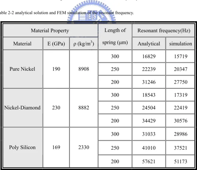
By equation (2.5) and FEM simulation, the resonant frequency of comb drive can be computed. The result is shown in Table 2-2.
Figure 2-1 the model the comb drive by Ansys. Table 2-2 analytical solution and FEM simulation of the resonant frequency.
Material Property Resonant frequency(Hz) Material E (GPa) ρ (kg/m3)
Length of
spring (µm) Analytical simulation
300 16829 15719 250 22239 20347 Pure Nickel 190 8908 200 31246 27750 300 18543 17319 250 24504 22419 Nickel-Diamond 230 8882 200 34429 30576 300 31033 28986 250 41010 37521 Poly Silicon 169 2330 200 57621 51173
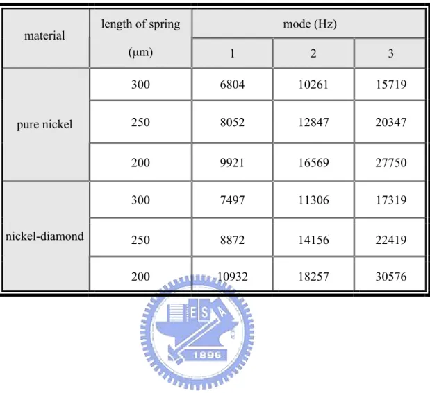
2.3 Modal Shape Discussion
By Ansys, the resonant frequency of comb drive is simulated. In the simulation results, it is found that the in-plane motion is the third mode. In other words, there are two modes with lower frequencies.
This phenomenon can be explained by the effective spring constant. In order to simplify the problem, the effective spring constant is considered as two parts: (in x direction) and Kz (in z direction). According to the dimension design of comb drive, Kz is less than Kx. The first mode and the second mode are torsional and out-of-plane. The effective spring constants of these two modes are contributed almost by Kz. The effective spring constants of torsional and out-of-plane motion are lower than in-plane motion. The lower effective spring constant gets lower resonant frequency. There are two modes with lower frequency before in-plane mode. The results are shown in Table 2-3.
(b)
(c)
Table 2-3 the resonance frequencies of pure nickel and nickel-diamond under different mode.
mode (Hz) material length of spring
(µm) 1 2 3 300 6804 10261 15719 250 8052 12847 20347 pure nickel 200 9921 16569 27750 300 7497 11306 17319 250 8872 14156 22419 nickel-diamond 200 10932 18257 30576
Chapter 3 Fabrication Process
3.1 Fabrication Process
The comb drive structure is shown in Figure 3-1. There are three main layers: (1) pad, (2) sacrificial layer, (3) structure layer. Here pad and structure layer are used nickel as the material. Photoresist (PR) and copper are the choices for sacrificial layer.
Figure 3-1 the structure of the comb drive.
3.1.1 Sacrificial Layer
Before coming to the fabrication process, the sacrificial layer must be determined. Considering the thermal expansion coefficient variation with nickel and the fabrication method, there are two materials available, PR and copper.
the rotation rate. It also provides good uniformity. The only thing that must be concerned is the hard bake of PR. Referring to Figure 3-1 and Figure 3-3, the PR sacrificial layers fail because of no hard bake or hard bake less. These damages occur at soft bake of next PR process. This problem can be solved by appropriate hard bake, but the hard bake causes the sidewall reflow. Fortunately, this phenomenon influences the post-process less.
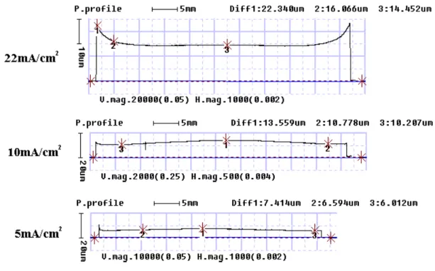
There is no reflow with Cu sacrificial layer. So it is easy to obtain vertical sidewall. The Cu sacrificial layer is shown in Figure 3-4. The uniformity is the biggest problem of this process. This Cu layer is deposited by electroplating. Comparing to PR, it is harder for electroplating Cu to obtain a uniform surface. From the profile figure in Figure 3-5, it is useful to obtain good uniformity by reducing the current density.
Comparing PR with Cu, PR process need less time than Cu process, but Cu sacrificial is more suitable for post-process than PR. To sum up, these two materials are both suitable utilized as the sacrificial layer.
Figure 3-3 PR sacrificial layer after soft bake (hard bake less).
Figure 3-5 profile of Cu sacrificial layer under different current densities.
3.1.2 Process Flow
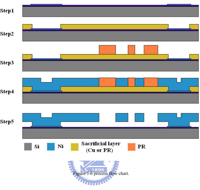
According to the mentioned above, the materials of main layers are decided. So the process flow can be determined and given below. The relative process flow chart is shown in Figure 3-6.
Step1: After RCA cleaning, wet oxide and LPCVD nitride are deposited on the silicon substrate. FH6400 is spun on the wafer and patterned by Mask#1. Sputtered Ti and Ni are lifted off by FH6400. Here, Ti is the adhesion layer and Ni is the pad material.
Step2: Cu sacrificial layer-
Sputtered Ti and Cu are lifted off by FH6400 which is patterned by Mask#2. AZ4620 patterned by Mask#2 is used as the mold of the Cu electroplating. This Cu layer is the sacrificial layer.
PR sacrificial layer-
FH6400 is spun on the wafer and patterned by Mask#2’ (inverse of Mask#2). Cu is sputtered as the seed layer after hard bake.
Step3: AZ9260 is spun on the wafer and patterned by Mask#3. This AZ9260 layer is the mold of the Ni electroplating.
Step4: Ni and Ni-Diamond are electroplated by using the Cu as the seed layer. Step5: For Cu sacrificial layer-
AZ9260 and Cu layer are removed by ACE and the solution of ammonia plus hydrogen peroxide individually. Finally, the sample is baked dry after IPA immersion.
For PR sacrificial layer-
AZ9260 and Cu seed layer are removed by ACE and the solution of ammonia plus hydrogen peroxide individually. Here the etching of the Cu seed layer must be well control. The structure may peel off because of the over etching. The FH6400 sacrificial layer is removed by PR stripper. At last, the sample is baked dry after IPA immersion.
Figure 3-6 process flow chart.
3.2 Photoresist Process
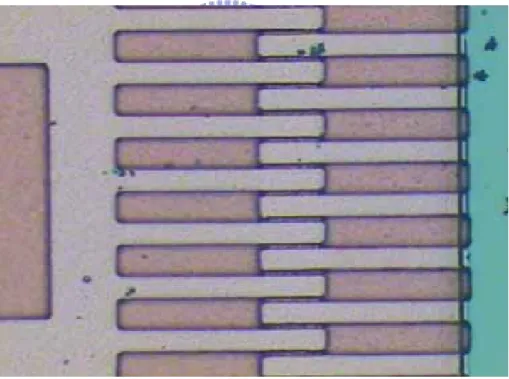
Before electroplating, there must be a good PR mold. The good PR mold is defined as the high aspect ratio, the vertical sidewall, and the less loss of linewidth. Here the high aspect ratio can be solved by using AZ9260.
It is found that there is serious linewidth loss of the comb gap when all parts are well developed. The result is shown in Figure 3-7. Before the PR is spun on, there is a step height between the anchor and sacrificial layer. After the PR is spun on, the thickness of the PR on anchor is thicker than on sacrificial layer. In order to develop the PR in anchor well, the developed time must be extended then the linewidth of the comb gap loses. This
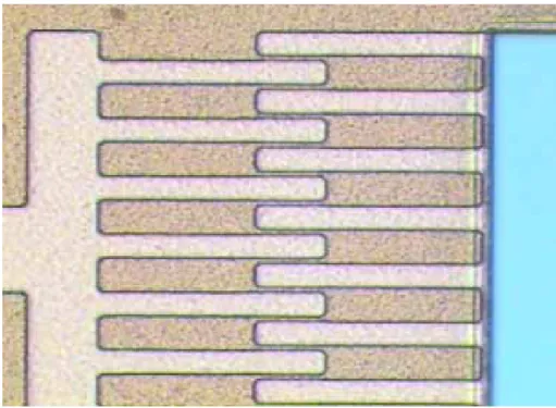
problem can be solved by using plasma etching. When the PR on sacrificial layer is well developed, the developing process stops. The residual PR on anchor can be removed by plasma etching. Plasma etching is anisotropic etching. Therefore, the linewidth of comb gap won’t be lost. But there is no such equipment available. By diluting the developer, the loss of the linewidth of comb gap can reduce. Comparing Figure 3-8 with Figure 3-7, there is a better comb gap by diluting the developer.
AZ9260 can also solve the problem of the vertical sidewall. As shown in Figure 3-9, the sidewall is about 80 degrees. This result is better than what made by AZ4620.
If the mold is much thicker than electroplating film, the sidewall will more close to 90 degrees. For example, the thickness of mold in 13µm shows better vertical sidewall than one in 7µm for the thickness of the electroplating film in 7µm.
.
Figure 3-8 AZ9260 after developed by diluting the developer (the original comb gap is 4µm)
3.3 Nickel and Nickel-Diamond Electroplating
Electroplating is the most important step in whole process. The quality of comb drive depends on the conditions while electroplating. Here no bending and no stiction structures are needed. By preliminary experiment result, the stiction phenomenon can be solved by IPA immersion. No bending structure depends on the residual stress of the structure and the residual stress depends on the factors of electroplating condition. There are too many factors to control the electroplating conditions. In order to finding out what the key point is, it seems useful to divide these factors into two parts. One is the electroplating solutions relative; the other is the operation condition relative.
The electroplating solution relative factors are simply defined as the quantities of the compositions and pH level. In the electroplating solution, there are nickel sulfamate, boric acid, nickel chloride, and additives. It is hard to obtain optimum situation by tuning the quantities of the compositions. So what can be done is following the commercial solutions. All the quantities of compositions are shown in Table 3-1. The pH level of the solution is kept in 4.0~4.3. The pH level of the solution which obeys Table 3-1 is at the range from 4.05 to 4.15. Sulfuric acid and ammonium hydroxide are used to counteract the solution if the pH level is over the range. The diamond nanoparticles with average diameter in 500nm are added into electroplating solution with concentration in 2g/L. The diamond nanoparticles have no influence with the pH level.
Current density, temperature, and ventilated system are the important parameters of operation condition. By changing current density and temperature, the different deposition rate and residual stress can be observed. These parameters are easier to control than those parameters of the electroplating solution relative.
Table 3-1 the quantities of compositions in the nickel electroplating solution.
additives composition Nickel sulfamate boric acid nickel chloride
EPC-30 NPA quantity 400mL/L 40g/L 5g/L 10mL/L 1~3mL/L
3.3.1 Setup of the Electroplating System
The electroplating system is shown in Figure 3-10. The system includes tank, cathode part, anode part, ventilated system, pump, and power supply. The sample is pasted on the cathode part. In Figure 3-12, there is a dummy part on the cathode except the sample. The dummy part is used to increase the total area. The sample area is about 1cm2. With 1.2mA/cm2 current density, the operation current is 0.0012A. This current is impossible for the power supply. For this reason given above, it is necessary to increase the total area. By using the dummy area, the total area can increase to 11cm2 and the operation current increase to 0.013A. This current is possible for the power supply.
The real nickel electroplating system is shown Figure 3-13. Because it needs heating during electroplating, the tank is immersed into the constant temperature water immersion system.
Figure 3-10 setup of the electroplating system.
(c) (d)
Figure 3-11 (a) tank; (b) cathode part; (c) anode part; (d) ventilated system.
Figure 3-12 the cathode part with sample.
Figure 3-13 the electroplating system.
3.3.2 Current Density Effect
Current density is defined as the current dividing by the effective area. According to the experimental result, it seems helpful to reduce the residual stress by reducing the current density. According to the figure in Figure 3-14 and Figure 3-15, there is less residual stress when reducing the current density.
Except reducing the residual stress, there is one more important phenomenon when the current density is lowered down. From electroplating point of view, current density indicates how many metal atoms are precipitated per area. So the deposition rate can be easy controlled by current density. Actually, the proportion of the deposition rate to the current density isn’t always the constant. Figure 3-16 shows the experimental result. The slope of low current density is sharper than high current density. The sharper slope indicates that the rate of electron transform into nickel is lowered down at low current density.
the suspension structure can be obtained for pure nickel electroplating. The proper current density for nickel electroplating is 1.2mA/cm2. This residual stress reducing effect is not effective at the current density less than 1.2mA/cm2. For nickel-diamond, the end of the spring still touches with the substrate. In other words, the residual stress is still serious at the same condition for nickel-diamond structure. Therefore, only reducing the current density is no use for nickel-diamond structure.
Figure 3-15 nickel electroplating with low current density (1.2mA/cm2).
Figure 3-16 current density-deposition rate for nickel electroplating.
3.3.3 Temperature Effect
By changing the operation temperature, it is found that the suspension nickel-diamond can be obtained. There are two reasons. One is that temperature causes geometry
deformation and the other is that temperature causes the variation of residual stress.
Based on the equation of the thermal expansion, the elongation of the beam grows with the increases of the temperature difference, the original length of the beam, and the thermal expansion coefficient. It is shown in the following equation:
T L L= 0α∆
∆ (3.1) Where ∆L, L0, α, and ∆T represent elongation, original length, thermal expansion coefficient, and temperature difference. In the standard nickel electroplating process, the operation temperature must be retained at 50 . If the room temperature is 25 , there is℃ ℃ 25 temperature difference. So there must be elongation under nickel electroplating ℃ process.
The spring beams of comb drive can be considered as long-short. According to the equation, the expansion deviation of long beam and short beam can be represented as Lcα∆T. Lc is represented as the difference between the long beam and short beam. The expansion deviation may cause the bending of spring beams. The dimension and the material are decided, so the expansion deviation is reduced only by decreasing the operation temperature.
But by heating the released sample to 80 , the ℃ bending effect is not serious. The result is shown in Figure 3-17. Except the geometry deformation, the changing of temperature also causes different residual stress.
(a) (b)
3.4 Results of Electroplating
As mentioned above, it is useful to achieve the suspension structure by reducing the current to 1.2mA/cm2 and lowering the operation temperature to 35℃. The structures are shown in Figure 3-18 and Figure 3-19. By pure nickel electroplating, there is a smooth surface. Next turning nickel-diamond electroplating, the surface of comb drive is dispersed by voids.
Except pure nickel and nickel-diamond, there is a test for nickel-CNT electroplating. It is found that the structure is still bending under the same fabrication process. The result of nickel-CNT electroplating is shown in Figure 3-20.
(c)
Figure 3-18 (a) full view; (b) spring part; (c) surface of comb drive by pure nickel
(a) (b)
(c)
(a) (b)
(c)
Chapter 4 Measurement and Discussion
4.1 Material Property Measurement
The suspension comb drive structure is fabricated by the process flow mentioned above. Although the electroplating solution is the same, the material by these operation conditions is different from Teh’s research. In Figure 4-1, it shows the diamond nano particles are not easy to be fu in Teh’s research. This phenomenon is different from the random distribution in Figure 3-19(c). In Shen’s research, the diamond nano particles induce the creaks and voids in the nickel film. There are only voids in Figure 3-19(c). The material properties may be different from Teh’s and Shen’s. So it is necessary to measure the material property.
(a) (b)
Figure 4-1 (a) TEM photo of nickel-diamond in Teh’s research[13]; (b) SEM photo of nicke-phosphorus-diamond in Shen’s research[14].
4.1.1 Measurement of CTE
By heating the sample, there is length difference between room temperature and higher temperature. Here the highest temperature is 350℃ and the heating process is recorded by
CCD.
According to the recorded film, each length of beam can be expressed as pixels. Using these pixels difference and substituting into equation (3.1), the CTE is shown in Table 4-1. This CTE measurement is at 350℃ because the pixel difference is hard to distingue at lower temperature.
The result shows that the nickel-diamond nanocomposite has higher CTE than pure nickel. This tendency is the same as the Teh’s researches.
Table 4-1 the results of CTE measurement.
number 1 2 3 4 5 L0(pixels) 363 363 359 362 362 L1(pixels) 364 364 360 363 364 ∆L(pixels) 1 1 1 1 2 ∆T(℃) 320 320 320 320 320 α(10-6/℃) 8.6 8.6 8.7 8.6 17.2 pure nickel average α(10-6/℃) 10.4 number 1 2 3 4 5 L0(pixels) 362 362 360 362 362 L1(pixels) 366 365 365 366 365 ∆L(pixels) 4 3 5 4 3 ∆T(℃) 320 320 320 320 320 α(10-6/℃) 34.5 25.9 43.4 34.5 25.9 nickel-diamond average α(10-6/℃) 32.9
4.1.2 Measurement of Young’s Modulus and Hardness
Young’s modulus is an important property and this property can be measured by nano indenter. By indenting the sample form surface to the setting depth, the relation of Young’s modulus and depth can be obtained. The results of pure nickel and nickel-diamond are shown in Figure 4-2 and Figure 4-3. One line represents the result of one location of the sample. According to the experiences, different location and depth get different Young’s modulus. So it is necessary to take more locations to get more reliable average results. There are sixteen locations taken and the depth is set at 700nm. The results show the Young’s modulus from surface to 700nm. By renouncing the curve with strange shape, the finial results are taken from 500nm to 700nm because it may be some problems at initial measurement. The curve with strange shape may be caused from slide of the needle. Except Young’s modulus, the hardness can also be obtained by nano indenter. The results are arranged in Table 4-2.
The diamond nano particles disperse randomly in nickel film and the diamond concentration of one location has some different from each other. Therefore, the property measurement of nickel-diamond gets larger deviation than pure nickel.
The results show that the Young’s modulus of nickel with diamond nano particles in it is improved from 173GPa to 217GPa.
(a) (b)
Figure 4-2 (a) Young’s modulus and (b) hardness of pure nickel.
(a) (b)
Table 4-2 the results arrangement of Young’s modulus and hardness.
property material
Young’s modulus (GPa) Hardness (GPa) average standard deviation average standard deviation pure nickel
173 6.57 4.5 0.35 average standard deviation average standard deviation nickel diamond
217 8.82 6.6 0.54
4.2 Resonant frequency measurement
The Laser Doppler Vibrometer (LDV) is used to measure the resonance. This instrument can observe the displacement under different frequency. When comb drive is operated under resonant frequency, it is easy to found large displacement. According to this concept, the resonant frequency can be found by the obvious displacement shift.
There are two main measurements of motion: in-plane and out-of-plane. LDV is an ideal tool for displaying out-of-plane displacement. It is impractical to measure in-plane motion since the Doppler shift is derived from a velocity vector normal to the plane of the moving surface. The problem of in-plane motion measurement can be solved by using stroboscopic video microscopy. The resolutions of in-plane and out-of-plane are 20nm and 0.5nm.
By preliminary test, the in-plane displacement of comb drive in this thesis is too small to observe. Although the comb drive is designed to move only in the in-plane direction, some residual out-of-plane motion exists that can be detected through the high sensitivity of the LDV sensor. Therefore the out-of-plane measurement is used to find the resonant frequency and the operation condition is set under 50V AC with 50V DC bias.
The displacements of comb drive made by pure nickel are shown in Figure 4-4. The frequency range is from 1kHz to 21kHz for the spring with 300µm in length. It seems that there is a main peak at 7~8kHz. This peak is the first mode. After this peak, there are two peaks combining from 17kHz to 20kHz. These two peaks may be the second and third modes. The peaks of second and third modes are not easy to recognize. So the measurement is focused on the first peak.
In order to find the more accurate position of resonant frequency, it is necessary to take more points on the possible location. Figure 4-5 is based on Figure 4-4 to take 30 points from 7kHz to 10kHz. It seems that the first mode of pure nickel comb drive is located at 8.034kHz. The same steps are applied on nickel diamond comb drive. Referring to Figure 4-6 and Figure 4-7, it is found that the first peak is located at 8.949kHz. The peak of
nickel diamond comb drive is not obvious. By the measurement results, it seems that the nickel diamond comb drive gets smaller displacement than the pure nickel one. Because the spring constant of nickel diamond one is larger the pure nickel one, the nickel diamond one gets small displacement under the same operation condition.
As shown in Table 4-3, the results measured by LVD are larger than the simulation results. This phenomenon can be explained by the spring size. The sidewall of simulation modal is vertical but the actual sidewall is about 80 degrees. It make the spring constant of actual comb drive larger than ideal one. So it is reasonable to get large resonant frequency by measurement.
0 0.1 0.2 0.3 0.4 0.5 0.6 0.7 0.8 0.9 1 1.1 0 5000 10000 15000 20000 Frequecy(Hz) Dispmacement(normalized)
Figure 4-4 Frequency-Displacement relation of pure nickel comb drive form 1kHz to 21kHz.
0 0.1 0.2 0.3 0.4 0.5 0.6 0.7 0.8 0.9 1 1.1 6000 7000 8000 9000 10000 11000 Frequency(Hz) Displacement(normalized)
0 0.1 0.2 0.3 0.4 0.5 0.6 0.7 0.8 0.9 1 1.1 0 5000 10000 15000 20000 25000 Frequency(Hz) Displacement(normalized)
Figure 4-6 Frequency-Displacement relation of nickel diamond comb drive form 3kHz to 22kHz.
0 0.1 0.2 0.3 0.4 0.5 0.6 0.7 0.8 0.9 1 1.1 6000 6500 7000 7500 8000 8500 9000 9500 10000 10500 Frequency(Hz) Displacement(normalized)
Table 4-3 resonant frequency deviation between simulation and measurement. first mode material simulation (Hz) measurement (Hz) pure nickel 6804 8034 nickel diamond 7497 8949 Improvement (%) 10.2 11.4
Chapter 5 Conclusion
The comb drives made by pure nickel and nickel diamond are demonstrated by electroplating. There are some important points in fabrication and measurement.
By reducing the current density and operation temperature, it is possible to eliminate bending in comb drive structure. Except the two parameters, there are many other conditions which can be tuning. For example, the composition and pH level of the electroplating solution are the tuneable parameters. Under 1.2mA/cm2 and 35℃, it is possible to get the structure with no bending.
The material properties are a little bit difference between different operation parameters. This is a serious problem for electroplating. In order to get comparable device, the comb drive made by pure nickel or nickel diamond is under the same operation conditions.
In the measurement side, there are many driving methods in the relative literatures. It seems that only one of these methods can drive the comb drive in this thesis. So it is needed to confirm the drive methods.
The dimension design is an important issue of comb drive manufacture. The dimensions of comb drive in this thesis are based on the fabrication ability, so it is hard to reduce the dimensions. According to the experiment experience, some related problems may be solved by reducing the dimensions. For example, if the width of spring is reduced, the thickness can also be cut down and the operation time can be diminished. If the thickness is much larger than the width of spring, the in-plane mode would occur before the out-of-plane mode and there is no coupling of the in-plane and out-of-plane mode. The linewidth also influence the electrostatic force. It is found that the electrostatic force of comb drive in this thesis is too small to drive comb drive because the gap of comb structure is too large. By reducing the gap of comb structure, the electrostatic force can be improved
effectively. So it is necessary to find another aligner which can get smaller linewidth for further research.
Reference
[1]W. C. Tang, T.-C. H. Nguyen, and R. T. Howe, “Laterally Driven Polysilicon Resonant Microstructure”, Proceedings IEEE MEMS, February, 1989, pp.53-59.
[2]M. Biebl, G.. T. Mulhern, and R. T. Howe, “In Situ Phosphorus-Doped Polysilicon for Integrated MEMS”, the 8th International Conference on Solid-State Sensors and Actuators, and Eurosensors IX. Stockholm, Sweden, June 25-29, 1995, pp. 198-201.
[3]Franke, A.E.; Bilic, D.; Chang, D.T.; Jones, P.T.; King, T.-J.; Howe, R.T.; Johnson, G.C. “Post-CMOS Integration of Germanium Microstructures” 12th IEEE Int. Conf. on Micro Electro Mechanical Systems (MEMS 99), Orlando, Florida, Jan. 17-21, 1999, pp. 630-637. [4]S.-A. Bhave, B.-L. Bircumshaw, W.-Z. Low, Y.-S. Kim, Albert P. Pisano, T.-J. King, and R.
T. Howe, “Poly-SiGe: A High-Q Structural material for Integrated RF MEMS”, Solid-State Sensor, Actuator and Microsystem Workshop Hilton Head Island, South Carolina, June 2-6, 2002, pp. 34-37.
[5]D. Gao, M.B.J. Wijesundara, C. Carraro, C.W. Low, R.T. Howe, and R. Maboudian, “High Modulus Polycrystalline 3C-SiC Technology for RF MEMS”, Proc. Transducers’03, The 12th International Conf. Solid-State Sensors & Actuators, pp. 1160-1163.
[6]B. Kim ; S. Park, H. Kim, K. Chun, D.-I. Cho, J.-W. Lee, H.-J. Lee ; W.-K, Seong, Y.-J. An, “MEMS Fabrication of High Aspect Ratio Track-Following Micro Actuator for Hard Disk Drive Using Silicon on Insulator” IEEE International Conference on Micro Electro Mechanical Systems, Jan. 1999, pp.53-56.
[7]K.-H. Jeong and Luke P. Lee, “A Novel Fabrication Method of a Vertical Comb Drive Using a Single SOI Wafer for Optical MEMS Application”, in Proc. 2003 Int. Conf. Solid-State Sensors and Actuators, pp. 1462-1465
for RF Application”, Proceedings of the 29th EuropeanSolid-State Circuits Conference, ESSCIRC 2003,Estoril, Portugal, September 16 - 18, 2003, pp. 607-610
[9]W.-T. Hsu and Clark T.-C. Nguyen, “Geometric Stress Compensation for Enhanced Thermal Stability in Micromechanical Resonators”, Proc. of 1998 IEEE Int. Ultrasonics Symposium, Sendai, 1998, pp. 945-948.
[10]A.D. Yalcinkaya, J.T. Ravnkilde, L.S. Johansen, O. Hansen, “Methods for Fabrication of Released Nickel Comb-Drive Devices on CMOS”, Transducers ’01, Digest of Technical Papers, Springer-Verlag, Munich 2001, pp. 600-603.
[11]K.-S. Teh, Y.-T. Cheng, and C. Sambucetti, “Selective Plating of Nickel Ceramic Composite Films for MEMS Application”, Proc. 15th Annual Int. Conference on Micro Electro Mechanical System, pp.384-387, Las Vegas, NV. USA, 2002, pp. 384-387.
[12]K.-S. Teh, Y.-T. Cheng, and L.-W. Lin, “Nickel Nano-Composite Film for MEMS Application”, the 12th International Conference on Solid State Sensors, Actuators and Microsystem, Boston, June 8-12, 2003, pp. 1534-1537.
[13]L.-N Tsai, G.-R. Shen, Y.-T. Cheng, W.-S. Hsu, “Power and Reliability Improvement of an Electro-Thermal Microactuator Using Ni-Diamond Nanocomposite”, the 54th Electronic Components and Technology Conference, June 1-4, 2004, Caesars Palace, Las Vegas, Nevada USA.
[14]G.-R. Shen, “Properties Enhancements of Ni-P-CNTs and Ni-P-Diamond Nanocomposites Films and the applications on MEMS device”, Thesis of Department of Electronics Engineering & Institute of Electronics, National Chiao-Tung University, June 2004.
![Figure 1-1 comb structures with spring beams on each side[1].](https://thumb-ap.123doks.com/thumbv2/9libinfo/8135473.166416/15.892.320.614.108.741/figure-comb-structures-spring-beams.webp)
![Figure 1-3 E/ρ-Diamond concentration [13].](https://thumb-ap.123doks.com/thumbv2/9libinfo/8135473.166416/18.892.178.769.117.500/figure-e-ρ-diamond-concentration.webp)