1590 IEEE TRANSACTIONS ON ELECTRON DEVICES, VOL. ED-34, NO. j, JULY 1987
on
Polycrystalline etilicon-Modeling and
Experiments
Abstruct-A theoretical model considering the effects of Fowlei-- Nordheim tunneling, image-force lowering, first-order trapping kimct- ics, impact ionization, and asperity-induced field enhancement has becm developed to investigate the ramp-voltage-stressed I-V characteristics of the oxide,films thermally grown on the polycrystalline silicon. From the ramp-voltage-stressed Z-V measurements, the important physical parameters such as average field-enhancement factor, effective total trapping density, trap capture cross section, recombination capture cross section, and dielectric breakdown field can be extracted.
Under a ramp voltage stress, it is shown that the serious asperity effect can lead to a larger leakage current and a weaker dielectric breakdown field, but the serious trapping effect may reduce the leak- age current and enlarge the dielectric breakdown field. Moreover, dry
0, oxidation at a higher temperature and steam oxidation at a lower temperature can result in a better quality poly-oxide because the as- perity-induced field enhancement is weakened and the electron trap- ping effect is slightly increased. Besides, high-temperature dry 0, (IX- idation can result in a smaller asperity effect as compared with ste;m oxidation, and the quality of the poly-oxide is deteriorated when the poly-Si substrate is heavily doped because the asperity effect is c:n- hanced.
S
I. INTRODUCTION
INCE THE OXIDE films thermally grown on poly-
crystalline silicon (named poly-oxide) have been
widely used in nonvolatile memory devices such as
EPROM and EEPROM devices, it is desirable to fabri- cate high-quality poly-oxide films as these devices are scaled down. The prerequisites for a high-quality oxide
film are smaller leakage current and stronger dielectric
field strength. However, these characteristics are con-
cerned with electron trapping [I]-[4], positive charge
generation, and asperity-induced field enhancement
[‘.I-
[l I]. Therefore, it is useful to develop a method so that
the poly-oxide films can be characterized both qualita- tively and quantitatively.
Ramp-voltage-stressed I-V measurement has been shown to be a useful technique to investigate the electmn
trapping
161,
[ 121, [13] and the dielectric field strength[13] of oxide films grown on a single-crystalline silicon
Manuscript received August 26, 1986; revised February 21, 1987. ‘This work was supported under grants from the Electronics Research and Ser- vice Organization, the Industrial Technology Research Institute, and the National Science Council, Republic of China.
The authors are with the Institute of Electronics, College of Engireer- ing, National Chiao-Tung University, Hsin-Chu, Taiwan, Republi,: of
China.
IEEE Log Number 8714645.
substrate. A simple model considering the effects of elec- tron trapping and electric field enhancement of the poly- oxide films has been developed [4], based on a combi- nation of the conventional Fowler-Nordheim conduction mechanism, first-order trapping kinetics, and nonuniform distribution of injection current. However, since the in-
terface between the poly-oxide and its electrode is ex-
tremely rough with various bumps, protuberances, and in- clusions, it is hard to determine the shape and, further, the dimensions (i.e., height and width) of the asperities.
In this paper, a theoretical model including the effects
of modified Fowler-Nordheim tunneIing, image-force
lowering, first-order trapping kinetics, impact ionization, and asperity-induced field enhancement has been devel- oped to analyze the ramp-voltage-stressed I-V character- istics of poly-oxide films. Based on this model, not only electron trapping and the dielectric field strength but also the field-dependent average field-enhancement factor per- taining to the poly-oxide films can be well evaluated. The most prominent feature of the developed model is that the determination of the field-dependent average field-en- hancement factor can be simply and accurately calculated from the experimental data without regard to the actual
shapes and dimensions of the asperities.
Moreover, poly-oxide films thermally grown in dry O2
and steam ambients at various temperatures have been
fabricated and analyzed theoretically. In addition, the ef- fects of doping types and concentrations in the poly-Si substrate upon the quality of the poly-oxide films have also been investigated and analyzed.
11. THEORETICAL MODEL
The carriers flowing through the poly-oxide layer under an external bias are mainly due to electron tunneling from the cathode electrode but not to the holes from the anode electrode because the holes have a larger barrier height and a heavier effective mass. The electrons injected into the conduction band of the oxide layer are gqverned by
the Fowler-Nordheim tunneling mechanism [ 141. Com-
pared with oxide films thermally grown on single-crystal- line silicon, the most prominent characteristics of oxide
films thermally grown on polycrystalline silicon are the
asperities and bumps located at the interface between the oxide layer and its electrode [4]-[ll]. Therefore, as the
WU AND CHEN: TRANSPORT PROPERTIES OF THERMAL OXIDE FILMS 1591
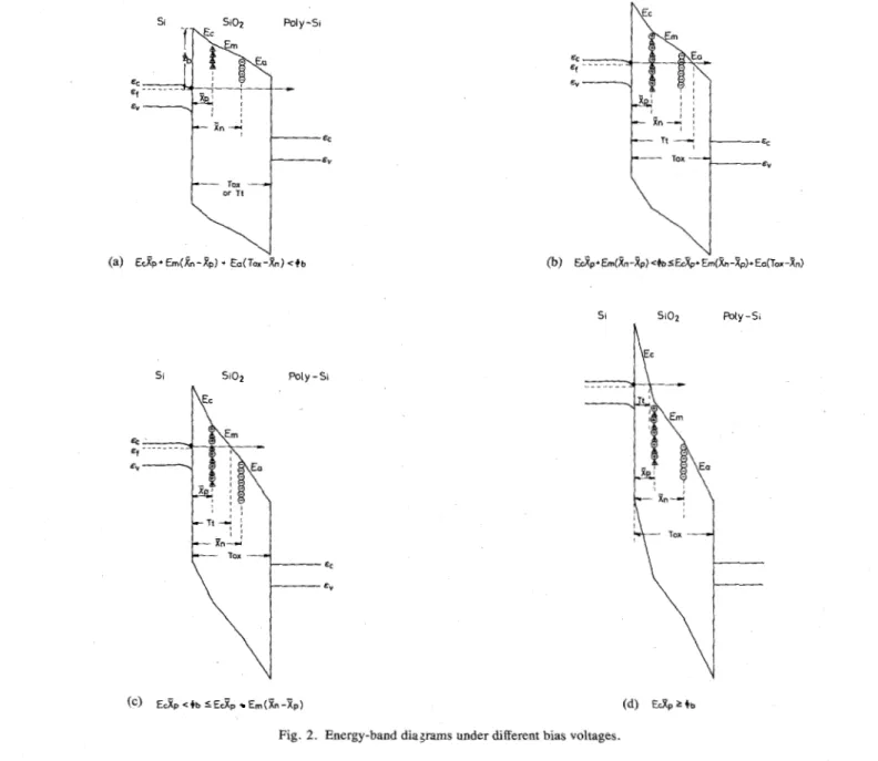
,?- ---e
-
Fig. 1. A theoretical model showing electron trapping, positive charge generation, and asperity-induced weak spots. 8 represents the trapped electron; 0 represents the positive ions generated from impact ioniza-
tion; 8 represents the neutral species; A represents the positive charges generated from the diffusion of neutral species and the broken bond at the interface.
electrons tunnel from the poly-Si film into the oxide con- duction band under high-field stress, aside from the elec- tron trapping and positive charge generation effects 1131, the asperity effect that results in local field enhancement should be considered. Fig. 1 shows schematically the
structure of the oxide films thermally grown on the poly-
Si in which the area with a locally enhanced electric field is called the weak spot, which is in contrast to the robust area. Besides the asperity effect, the electric field en- hancement may be due to nonuniform trap distribution, impurity segregation at the poly-Si grain boundary re- gions [ 151
,
highly mobile positive ions [ 161, [ 171,
and, especially, locally thin areas.The energy-band diagrams describing the weak spots and the robust area under different electric fields are shown in Fig. 2(a) through (d). Following previous concepts [ 131, [ 181, the electron traps and the trapped electrons are
assumed to be distributed uniformly in a plane that is par-
allel to the cathode-electrodelpoly-oxide interface with a
distance represented by the trapped electron centroid
z,,.
Similarly, the generated positive ions are assumed to be distributed in a plane that is closer to the cathode-elec- trodelpoly-oxide interface with a distance represented by
the generated positive ion centroid
xp.
In addition, thepositive charges aggregated near the cathode electrode within the robust area and the weak spots are assumed to be resulted from the diffusion of neutral species such as
atomic hydrogen [ 191-[2 11 or excitons [22] created by
bond-breaking through energetic avalanche-injected elec- trons and trapped by the dangling bonds at the interface as well as the broken bond at the interface during the pas- sage of heating electrons [23]-[25]. Furthermore, the positive ions generated from band-to-band andlor trap-to-
band impact ionization are assumed to be amassed near
the cathode electrode within the weak spots due to the
locally enhanced electric field.
Considering the effect of electric field enhancement, the Fowler-Nordheim tunneling current density across the potential barriers shown in Fig. 2(a) through (d) has the following form:
where m* is the effective mass of the tunneling electrons
in oxide and is assumed to be 0.5 m; fi is Planck's con-
stant divided by 2n; q is the electronic charge;
E,
( t ) isthe cathode electric field; E is the average electric field
across the oxide layer; p ( E ) is the average field-enhance-
ment factor, which
is
field-dependent; %b( p, E , ) is thebarrier height, which considers the image force lowering
effect; and
Tp
is the tunneling probability.The barrier height including the image-force lowering
effect is given by
where E,, is the dielectric permittivity of the oxide and
abO
is the intrinsic barrier height.The tunneling probability calculated by using the WKB
approximation has the following relations:
1) For
*$
2 % ( p , E c ) / p ( E )where E,,, ( t j is the electric field in the middle region and
+% = E c ( t ) Z p
+
E m ( t j ( X n-
Z p ) .
3) For
+xn
<
@ b ( p , E , ) / p ( E ) 51592 IEEE 3XANSACTIONS QN ELECTRON DEVICES, VOL. ED-34, NO. 7, JULY 1987
I
poly -Si
EC
e"
Cc) Ecxp C)b C E& Em(xn - x p ) (d) E c X p r t b Fig. 2. Energy-band diaqams under different bias voltages.
Note that E , ( , t ) and E, ( t ) are correlated to the cathode
electric field
E,
( t ) via the following equations:where V,( t ) is the applied voltage, which is equaI to y t
for the ramp-voltage-stressed I-V measurement and y is
the ramping rate (in volts per second); &s is the work
function difference between two electrodes; n , ( t ) is the
density of the trapped electrons at
x,;
and 0: ( t ) is thedensity of the effective holes at
zp.
The electron trapping effect considering the first-order trapping kinetics can be written as
where Nt and 0, are the total trapping density and the trap
capture cross section of the traps, respectively.
The total positive ions 6; ( t ) generated from the impact
ionization process for the four conditions shown in Fig.
2(a) through (d) can be written as 1) For
*$
2 %( P, & ) / P ( WW U AND CHEN: TRANSPORT PROPERTIES OF THERMAL OXIDE FILMS 1593
and
and
4, For @Tax
<
@ b ( p 7 E c ) / ' ( E )e;
( t ) = 0. (17)Note that cyo and H are constants pertaining to the impact
ionization coefficient cy that has the form 01 = cyo exp
( - H/E ), where E is the electric field and T, is the tun-
neling distance.
Considering the electron trapping (or recombination)
induced by these positive ions, a rate equation is yielded as follows [ 131 :
e:
( t ) =e:
( t ) - n i ( t ) (19)where uj is the recombination capture cross section and
ni ( t ) is the density of the recombined electrons. Note that
the initial conditions for (10) and (18) are n, ( t = 0 ) and
ni ( t = 0 ) = 0, respectively.
The total current across the oxide layer consists of the
displacement current, the Fowler-Nordheim tunneling
currents through the weak spots and the robust area, and the current due to the movement of the electrons gener-
ated from impact ionization, i.e.,
+
A & j r ( t )+
A w R w j w ( t ) (20)where Cox is the dielectric capacitance of the oxide film;
A, and A, are the mask areas of the weak spots and the
robust area, respectively; R, and Rr are the ratios of the actual injection area to the mask area of the weak spots and the robust area, respectively; j , ( t ) and j , ( t ) are the Fowler-Nordheim tunneling current densities through the
weak spots and the robust area, respectively; and
[de: ( t ) / d t ] , and [de: ( t ) / d t ] , are the electron gener- ation rates due to impact ionization within the weak spots and the robust area, respectively.
For the oxide films thermally grown on the poly-Si sub- strate, it can be assumed that the total area is composed
of the miscellaneous bumps, protuberances, and inclu-
sions due to the grains formed within the poly-Si substrate so that the robust area is actually absent. Therefore, the total current across the poly-oxide layer becomes
where A is the total mask area and
X
is the ratio of theactual injection area to the total mask area.
The Z-V characteristics of the poly-oxide layer can be
obtained by combining (1) through (21). Since these
equations form a nonlinear system, it is necessary to solve
them by using the numerical method.
111. COMPUTER SIMULATIONS AND DISCUSSIONS
A computer program using the fourth-order Runge- Kutta-Gill numerical method was set up to simulate these
nonlinear differential equations. In addition to electron
trapping and recombination as well as the dielectric
breakdown field concerned with the SiOz films grown on
the single-crystalline silicon substrate [ 131, the electric
field enhancement of the poly-oxide layer due to the as- perity effect deserves noting, especially when the samples are biased by a ramp voltage.
A. Average Field-Enhancement Factor
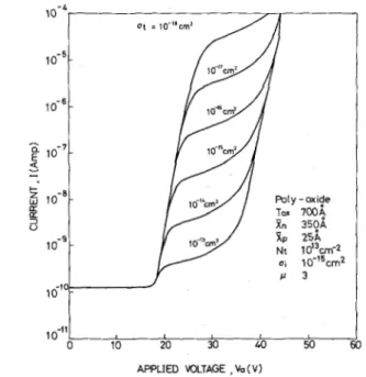
Fig. 3 shows the simulation results for the Z-V charac-
teristics of a poly-oxide layer with a thickness of 700 A.
The basic physical parameters used in Figs. 3 through 7
are listed in Table I, in which the constants a0 and H a r e
obtained from the impact ionization coefficient of the ox-
ide [26]
,
[27]. As can be seen, the harmful effects of fieldenhancement are the larger leakage current and the weaker
dielectric field strength accompanied by the increase of the field-enhancement factor. Defining the starting elec- tric field E, to be the electric field that the Fowler-Nord- heim tunneling current surmounts the constant displace-
1594 IEEE 'TRANSACTIONS ON ELECTRON DEVICES, VOL. ED-34, NO. I , JULY 1987
lo-"
0 20 40 Eo 80 1
APPLIED VOLTAGE ,Va (V) AVERAGE FIELD ENHANCEMENT FACTOR, P
Fig. 3. Computer simulations using the average field-enhancement factor Fig. 4. Starting electric field versus average field-enhancement factor for as a parameter for the 700-A poly-oxide layer. the 700-A poly-oxide layer.
700 350 25 1013 L 4 ~ 1 0 - ~ 1 3 3.3*106 78
ment current, the relationship governing the starting elec- tric field and the average field-enhancement factor can be
deduced from Fig. 3 and the result is shown in Fig.
4.
The very large slope of the curve shown in this figure as
the average field-enhancement factor increases a little above unity indicates that the field enhancement is very sensitive when the electrode deviates slightly from the planar structure; however, the sensitivity attains satura-
tion at the large average field-enhancement factor region
(say above
5 ) .
B. Trap Capture Cross Section
Fig. 5 shows the simuIation results for the poly-oxide
film with an average field-enhancement factor of 3 and a
trap capture cross section a, ranging from to IO-''
cm2. Similar to the results concerned with the Si02 film
grown on the singie-crystalline Si substrate [13], the mag..
nitude of the trap capture cross section o, pertaining to the poly-oxide films can be determined from the level of the: trapping ledge. A larger trap capture cross section lead!; to a faster electron trapping rate, which in turn lowers the cathode and middle electric fields and thus lessens thr: leakage current.
C. Effective Total Trapping Density
Fig. 6 shows the simulation results for a poly-oxide film with an average field-enhancement factor of 3 and an ef-
fective total trapping density N , ranging from 1 X 10" to
5
X l O I 3ern-'.
It is shown that a larger effective totaltrapping density N2 results in a smaller leakage current
and a stronger dielectric field strength. This fact is due to decreases of the cathode and middle electric fields with an amount proportional to the density of the trapped elec-
trons as revealed from (7) and (8); consequently, the
Fowler-Nordheim tunneling current is lessened. More- over, since the trapping ledge exhibits a distinct shape as
the effective total trapping density N, changes, as a result,
the magnitude of the effective total trapping density Nt can
be deterinined from the trapping ledge of the experimental measurements.
The simulation results for the breakdown field of poly-
oxide films with an effective total trapping density Nt and
an average field enhancement factor p as parameters are
shown in Fig. 7. As depicted from this figure, the asper-
ity-induced field enhancement weakens the dielectric field
strength and the weakening rate is doubled even though
the average field-enhancement factor p is increased from
1 to 2. Additionally, the dielectric field strength is en-
hanced as the effective total trapping density Nt is in-
creased. This phenomenon is especially prominent when
the effective total trapping density is above 1 X 1013 cm-2.
IV
.
EXPERIMENTAL PROCEDURE AND MEASUREMENTSSilicon p-type wafers of ( 100 ) orientation with a re-
sistivity of about 10 9
-
cm were used as the starting ma-terials. After the standard cleaning process, the Si02 layer
with a thickness of about 2500
A
was thermally grownWU AND CHEN: TRANSPORT PROPERTIES OF THERMAL OXIDE FILMS
1 o - I l T
0 10 20 30 40 50 M)
APPLIED VOLTAGE , Va(V)
Fig. 5 . Computer simulations using the trap capture cross section as a pa- rameter for the 700-A poly-oxide layer.
0 20 40 60 80 100
APPLIED VOLTAGE , Va ( V I
Fig. 6 . Computer simulations using the-effective total trapping density as a parameter for the 700-A poly-oxide layer.
were deposited on the oxide layer by thermal decom- position of silane in a low-pressure chemical-vapor dep- osition (LPCVD) reactor operated at 650°C. Some wafers were doped with phosphorus at 1000°C for 10 min using the P0Cl3 source; the others were implanted with phos-
phorus and boron ions with doses from 10" to l O I 5 cm-'
at 100 and 90 keV, respectively. Thermal oxidation of the
poly-Si films was performed at various temperatures rang-
ing from 900 to 1100°C in dry 0, and steam ambients.
For the samples with the top-electrode made of poly-Si, a second layer of poly-Si was deposited on the wafers and then doped with phosphorus. A pure AI film was evapo- rated onto the wafers by using a resistive tungsten fila- ment in a vacuum system. The deposited A1 film was then
0 , ' I I
10'2
1013 1
EFFECTIVE TOTAL TRAPPING DENSITY , N t ( c ~ n - ~ )
1595
14
Fig. 7. Breakdown field versus effect total trapping density with the av- erage field-enhancement factor as a parameter.
AI -gate Poly -Si gate Fig. 8. The structures of the finished samples.
photoengraved and etched to form the contact pattern. Fi- nally, the wafers were sintered in forming gas at 450°C
for 20 min. The finished structures are shown in Fig. 8 .
The average thickness of the poly-oxide layer was mea- sured by an interferometer. The ramp-voltage-stressed I-
V
characteristics was measured by using a Hewlett-Pack-ard 4140B picoammeter controlled by a desk-top com-
puter. A scanning electron microscope (SEM) also was
used to observe the surface morphology of the test sam- ples.
V . EXPERIMENTAL RESULTS AND COMPUTER
SIMULATIONS
A . Determination of the Average Field-Enhancement Factor
The ramp-voltage-stressed I- V characteristics of SiO,
grown on a single-crystalline Si substrate with an average
field-enhancement factor ,u equal to unity have been well
simulated [13]. However, for the poly-oxide films, ramp-
voltage-stressed I-V characteristics cannot be simulated
by using a single average field-enhancement factor be- cause the dimensions of the asperities are extremely ran-
1596
APPLIED VOLTAGE , Vo ( V )
(a)
Poly -Si Gate
1.1
3.5 4.0 4.5 5.0 5.5 6.0 6.5 7.0 7.5 8.0
ELECTRIC FIELD, E ( M V l u n ) (b)
Figd 9. (a) The ramp-voltage stressed Z-V characteristic curves for the 4.50- A poly-oxide layer under the bottom- and top-electrode injections and the computer simulations showing the method to determine the average field enhancement factors; (b) the average field enhancement factors f:x-
tracted from the curve shown in (a).
dom and complicated and the trap distribution is nonuni- form: thus, the average field-enhancement factor should be field-dependent. This can be clarified from Fig. 9(a) where the ramp-voltage-stressed Z-V characteristics of .:he
45OO-A poly-oxide layer are simulated by changing ;he
average field-enhancement factor. Note that the bottam- and top-electrode injections represent the injection of electrons into the poly-oxide film from the bottom elec- trode and the top electrode, respectively. From the inrer- sections of the simulated curves with the experimental curves, the average field-enhancement factor can be de- termined and the results are shown in Fig. 9(b).
It is clearly seen that the field enhancement is larger for bottom-electrode injection than for top-electrode in: ec-
LKAN&4LIIUN> U N hLOLlKUN UEVILOS, V U L . ED-34, NU. I , J U L Y 1 Y X 1
tion. We attribute this phenomenon to the serious texture roughness, such as the bumps and protuberances of the bottom interface resulted from locally enhanced oxidation at the grain boundaries. On the other hand, the average field-enhancement factor is found to be reduced as the electric field increases. The elements affecting the aver- age field enhancement of poly-oxide films include asper- ity and electron trapping effects. In order to extract the average field-enhancement factors resulting mainly from the asperities, the Fowler-Nordheim tunneling region of
the Z-V curve as shown in Fig. 9(a), which always ap-
pears before the appearance of the trapping ledge as shown
later in Fig. 10, must be used. As the applied voltage
across the poly-oxide film increases, the emitting area of ,the cathode electrode will increase in a nonlinear fashion due to the enlargement of the emitting area pertaining to the asperities with a larger field-enhancement factor cou- pled with the appearance of the asperities with a smaller field-enhancement factor. This fact would lead to a smaller
average field-enhancement factor [4], [28]-[30]. There-
fore, the decrease of the average field enhancement factor with the increase of the electric field can be explained.
B. Electron Trapping and Positive Charge Generation
Electron trapping and positive ion generation have been
found in SiOz film under a high field stress [ 181-[25]. In
order to observe the electron trapping and the positive'ion
generation in the poly-oxide layer, a constant current with
a density of 2.86 X A/cm2 was used to stress the
samples for 90 s which is very near the average time to
breakdown of 92 s. Then, thermal detrapping at 350°C
for 30 min was performed to remove the trapped electrons
from the poly-oxide film so that the positive ions that are left could be measured. Ramp-voltage-stressed 1-I/ mea- surements were performed by increasing linearly the ap-
plied voltage from 0 V to the point where dielectric break-
down takes place. Fig. 10 shows the experimental results
for the 390-A poly-oxide film. It should be noticed that the five curves were obtained by measuring five different
samples. After stressing, the measured I-I/ curve ( b ) is
shifted positively to the fresh one ( a ) . This suggests that
the electron trapping occurs during a constant current stress. After stressing and detrapping, the measured Z-V curve ( c ) shifts negatively to the fresh one, which is at- tributed to the enhanced cathode field by the left positive ions. On the other hand, when a reverse bias is applied to the stressed and thermally detrapped sample, the mea-
sured 1-V curve (e) is found to be smaller than the fresh
one ( d ) . Since the cathode electric field can be enhanced with a magnitude of (qe? ( t ) ,/eox) ( 1
-
xp/
Tax) due to positive ion accumulation, it can be concluded that the positive ions generated under a high-field stress are ag- gregated near the cathode electrode. The smaller leakage current in the 1-V curve ( e ) when compared with curve( d ) is due to the new traps formed by the left positive ions near the anode electrode. This fact lowers the cathode electric field and leads to a smaller tunneling current.
W U AND CHEN: TRANSPORT PROPERTIES OF THERMAL OXIDE FILMS 1597
Poly-oxide Thickness (mi)
Mask Area ( 1 . 4 ~ 1 O - ~ c m ~ l 1 6 6 (cl After StreslDetrap (3MmC.30min)
(bl After Stress(2.857x10⁴A/c~, Sosec CURRENT, 1 (A) (a) Before Stress
c
I(d) Before Stress
le) After StresslDetrap(350?.30min)
Top-electrode Injection
APPLlER VOLTAGE , Va ('4)
Fig. 10. The ramp-voltage-stressed I-Vcharacteristic curves for the 390- A poly-oxide layer with and without stressing and detrapping.
Taking the electron trapping and positive charge genera-
tion effects of the thin SiO, films into account [ 131, [ 181,
1271, it is interesting to find that the poly-oxide films have the same effects as the thin Si02 films grown on single- crystalline substrates.
C . E$ects of Oxidation Ambients
Fig. l l ( a ) and (b) shows the ramp-voltage-stressed
1-I/ characteristic of oxide films thermally grown on po-
lycrystalline Si films at different temperatures in dry O2 and steam ambients, respectively. Note that the top elec- trode is made of A1 and the samples are biased for bottom-
electrode injection. The average field-enhancement fac-
tors ,u ( E ) extracted from these figures are plotted
in
Fig.ll(c). In addition, the physical parameters used in the
theoretical simulations are listed .in Table 11. The values
of the barrier height and the work function difference
q5ms used in the calculations are chosen to be 3.15 and 0.2
eV [5], respectively. The trapped electron centroid
xa
isassumed to be one half of the poly-oxide thickness to
avoid the highly complicated situations concerned with
each sample. The generated positive charge centroid
xp
isassumed to be 25
A.
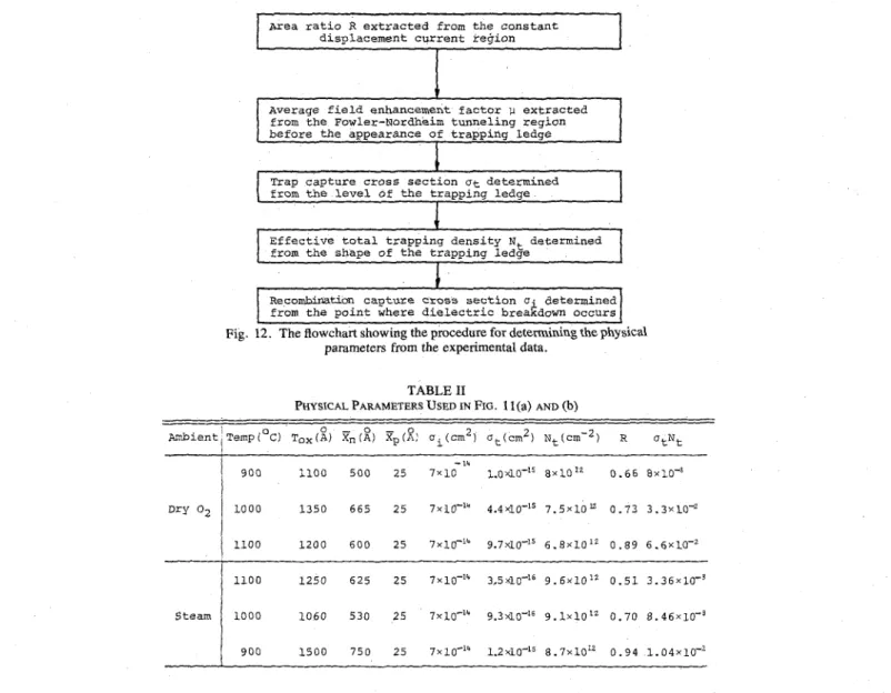
Moreover, the procedure for extract-ing the physical parameters ( R , p ( E ) , a,, N,, and a i ) of
the poly-oxide film is shown in Fig. 12. Since the actual
area €or Fowler-Nordheim tunneling from the irregular
asperities is correlated to the magnitude of current flow in a complicated manner, our calculations are performed by
fixing the area ratio R to a value determined from the dis-
placement current region where the current is approxi- mately proportional to the actual area. The trap capture
cross section a, and the effective total trapping density N ,
are determined from the level and shape of the trapping
ledge in the ramped 1-V characteristics, respectively, as
clearly shown in Figs. 5 and 6 . The recombination cap-
ture cross section ai is determined from the point where the dielectric breakdown takes place [ 131. Finally, the
product of the trap capture cross section a, and the effec-
tive total trapping density N , is used to indicate the degree
of the electron trapping effect.
Several important aspects addressed from these figures are:
1) The asperity-induced field enhancement for
the
poly-oxide films grown in dry O2 ambient is reduced greatly as
the oxidation temperature increases, while a reverse trend is obtained for the poly-oxide films grown in steam am- bient. Furthermore, when the oxidation temperature is
equal to or larger than lOOO"C, the dry O2 oxidation leads
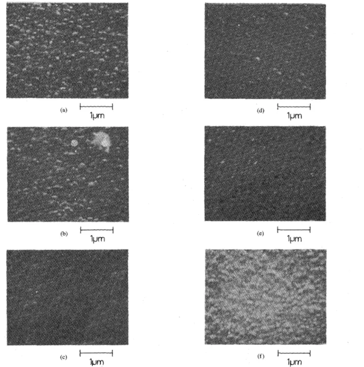
to a smaller field-enhancement factor than the steam oxi- dation. The surface morphologies of these poly-oxide lay-
ers can be observed from the SEM photographs shown in
Fig. 13. It can be seen that the dimensions of the asperi-
ties are larger for higher oxidation temperatures. Accord-
ing to the grain size growth mechanism
1311,
the grainsize is enlarged as the oxidation temperature increases. However, the asperities with a larger height-to-width ra-
tio are attached to the smaller grain size for dry O2 oxi-
dation and the larger grain size for steam oxidation. For
dry O2 oxidation, the lower oxidation temperature leads
to surface-reaction-controlled oxidation, which gives lin-
ear increase in the oxide thickness (To,[) with respect to
the oxidation time (t). However, a parabolic increase of the oxide thickness with the difision-controlled relation-
ship To, oc is expected for a higher oxidation temper-
ature. Therefore, the oxidant can penetrate more deeply into the grain boundaries at lower oxidation temperature,
resulting in a larger height-to-width ratio. For steam ox-
idation, the grain growth is as severe as compared to that of dry 0, oxidation and, furthermore, the faster oxidation rate pertaining to higher temperatures causes the oxidant to penetrate deeper into the grain boundaries. This gives a larger height-to-width ratio of the asperities at higher oxidation temperature.
2) The trapping effect becomes more prominant for the
poly-oxide films grown in dry O2 ambient at higher oxi- dation temperature, whereas a reverse trend is found for
1598 IEEE TRANSACTIONS ON ELECTRON DEVICES, VOL. ED-34, NO. 7, JULY 1987 Dry 02 Oxidation Bottom-Electrode Injection 0 X A Experimental Data 0 1 2 3 4 5 6 7 ELECTRIC FIELD , E ( MV I cm ) (a) o X A Experimental Data 0 1 2 3 4 5 6 ELECTRIC FIELD, E (MVlcm) (b) 1 l3
r---
----
-
Dry 02 Oxidation Steam Oxidation 2 ( . 1 . 1 1 1 . 1 1 1 . 1 . 1 ' 0 0.5 1.0 1.5 2.0 2.5 3.0 3.5ELECTfIIC FIELD , E(MVlcm) (c)
Fig. 11. The ramp-voltage-stressed I-V characteristic curves and theoretical simulations for the poly-oxide films grown in (a) dry O2 and (b) steam ambients at different temperatures; (c) the average field enhancement factors extracted from the curves shown in (a) and (b).
steam oxidation. Considering the traps originated from the
dopants, the oxidation rate of steam oxidation is faster
than the phosphorus diffusion rate; and this trend is more obvious at a lower oxidation temperature; therefore, the
phosphorus .dopants are apt to be trapped in the grown
oxide, resulting in a more serious trapping effect. For dry
O2 oxidation, the phosphorus dopants may diffuse into the
unoxidized poly-Si film and the diffusion rate is faste.r at higher temperatures. The increase of the phosphorus con- centration in the poly-Si film can enhance the oxidation rate; thus, more phosphorus dopants may be trappe'i in
the grown oxide once the oxidation rate overcomes the phosphorus diffusion rate, which can lead to a more se- rious trapping effect.
3) The recombination capture cross section is about the
same for various oxidation ambients and temperatures.
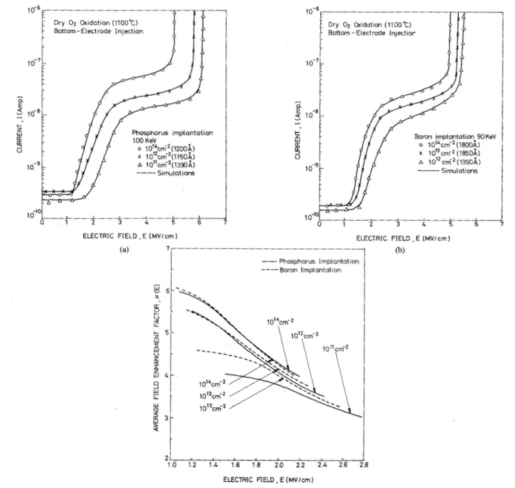
D. Efects of Doping Concentration
The, ramp-voltage-stressed I-V characteristics of poly-
,oxide implanted with different phosphorus and boron
doses are shown in Fig. 14(a) and (b), respectively. Fig.
W U AND CHEN: TRANSPORT PROPERTIES OF THERMAL OXIDE FILMS 1599
Area ratio R extracted from the constant
displacement current re9ion
1
I
Average field enhancement factor i-1 extracted
from the Fowler-Nordheim tunneling region before the appearance of trapping ledge
I
Trap capture cross section ut determined
from the level of the trapping ledge I
Effective total trapping density N determined from the shape of the trapping led$e
Fig. 12. The flowchart showing the pbcedure for determining the physical parameters from the experimental data.
j
900-
I4 1100 500 25 7x10 l . o ~ l O - ' ~ 8 x 1 0 " 0.66 P x ~ O - ~ Dry o2 1100 1200 600 25 7x10-" 9.7x10-" 6 . 8 ~ 1 0 ' ~ 0.89 6.6x10-' 1 0 0 0 1350 6 6 5 25 7 ~ 1 0 - l ~ 4.4~10-l~ 7 . 5 ~ 1 0 " 0.73 3.3x10-' 1100 1250 6 2 5 2 5 7x10-I' 3 . 5 ~ 1 0 - ' ~ 9 . 6 ~ 1 0 ' ~ 0.51 3.36xlO-' Steam 1000 1 0 6 0 5 3 0 25 7 ~ 1 0 - l ~ 9.3~10-'~ 9 . 1 ~ 1 0 ' ~ 0.70 8 . 4 6 ~ 1 0 - ~ 900 1500 750 25 7 ~ 1 0 - l ~ l.2~lO-'~ 8.7~10" 0.94 1.04~10-~tor p ( E ) and Table III lists the physical parameters used
in the theoretical calculations. As can be seen from these
figures, the phosphorus and boron doses lead to similar
trends in the I-I/ characteristics. The effects can be sum-
marized as: 1) The heavier doping results in a more seri-
ous asperity effect, which is ascribed to the faster oxida-
tion rate occurring at the grain boundaries of the heavily doped poly-Si films. 2) The trapping effect is slightly re- leased as the doping increases. 3) The recombination cap- ture cross section shows small differences for various do- pants and concentrations.
Note that the electron capture probabilities deduced
from, grown poly-oxide films vary from to
which are much larger than those ( 10-5-10-6) deduced
from thin thermal oxide films grown on silicon substrates
1131, [32], The major reasons are due to the larger thick-
nesses ( 1000-2000
A)
of the grown polyoxide films andthe properties of polysilicon substrate. VI. CONCLUSIONS
In this paper, we have proposed a theoretical model to
characterize poly-oxide films under different process con- ditions. Several important effects such as Fowler-Nord-
heim tunneling, image-force lowering, first order trapping kinetics, impact ionization, and asperity-induced field en- hancement are considered in this model. Based on this model, the average field-enhancement factor describing the asperity effect can be well evaluated. Some important conclusions obtained from the theoretical simulations are: 1) The serious asperity effect can enlarge the leakage cur-
rent and then weaken the dielectric field strength. 2) The
larger effective total trapping density can enhance the die- lectric field strength and then reduce the leakage current.
3) The larger trap capture cross section can yield a faster
trapping rate so that the leakage current is reduced.
The electron trapping and the positive charge aggrega- tion near the cathode electrode under a high-field stress
have been observed by using constant current stress, ther-
mal detrapping, and ramp-voltage-stressed I-V measure- ments. The asperity effect has been found to be more se- rious for the poly-oxidelbottom-electrode interface when compared with the poly-oxideltop-electrode interface. It
is found that the oxide films grown in dry O2 ambient
show a smaller leakage current and a stronger dielectric field strength as the oxidation temperature increases, due
to the increase of the trapping effect and the decrease of
1600 IEEE “’RANSACTIONS ON ELECTRON DEVJCES, VOL. ED-34, NO. I, JULY 19x7
Fig. 13. The SEM photographs showing the surface morphology O F the poly-Si films on which the poly-oxide layers have been removed for dry O2 oxidation at (a) 900°C, (b) 1000°C, and (c) llOO”1:; for steam oxidation at (d) 900”C, (e) 1000°C, and (f) 1100°C.
for the poly-oxide grown in steam ambient. For poly-Si
films implanted with different phosphorus and toron doses, a common trend shows that heavier doping car, lead to a larger leakage current and a weaker dielectric field strength, due to the increase of the asperity effect.
ACKNOWLEDGMENT
Special thanks are given to Dr. C . T. Shih and G. C .
Chang for their stimulating discussions. REFERENCES
[l] D. J . DiMaria, D. R. Young, and D. W . Ormond, “Use of dectron- trapping region to reduce leakage cnrrents and improve breakdown characteristics of MOS structures,” Appl. Phys. Lett., vol. 31, pp.
680-682, NOV. 1977.
[ 2 ] H. S . Lee and C. H. Feng, “High-electric-field-generated electron traps in oxide grown from polycrystalline silicon,” Appl. Phys. L e t t . ,
vol. 37, pp. 1080-1082, Dec. 1980.
[3] P. A. Heimann, S. P. Murarka, and T. T. Sheng, “Electrical con- duction and breakdown in oxides of polycrystalline silicon and their correlation with interface texture,” J. Appl. phys., vol. 53, pp. 6240- 6245, Sept. 1982.
141 G. Groeseneken and H. E. Maes, “A quantitative model for the con- duction in oxides thermally grown from polycrystalline silicon,” IEEE
Trans. Electron Devices, vol. ED-33, pp. 1028-1042, July 1986.
[5] D. J . DiMaria and D. R. Ken, “Interface effects and high conductiv- ity in oxides grown from polycrystalline silicon,” Appl. Phys. Lett., vol. 27, pp. 505-507, Nov. 1975.
[ 6 ] R. M . Anderson and D. R. Ken, “Evidence for surface asperity mechanism of condcctivity in oxide grown on polycrystalline sili- con,” J . Appl. Phys., vol. 48, pp. 4834-4836, Nov. 1977.
[7) E. A. Irene, E. Tierney, and D. W. Dong, “Silicon oxidation studies: Morphological aspects of the oxidation of polycrystalline silicon,” J.
WU AND CHEN: TRANSPORT PROPERTIES OF THERMAL OXIDE FILMS 1601 Dry 02 Oxidation (1100 C) Bottom-Electrode Injection 1 o - ~
-
E
5 10-8 I c Z LL LC 3 W Phosphorus implantation o 0 10"cm-2(12001\) 10'' A 10"~m-~(13901\) x 10'2crn~2(1150~)-
Sirnulatiom 1 6 ' O 0 1 2 3 4 5 6 ELECTRIC FIELD, E ( M V / c m )Boron implantation 9OKeV
0 1 2 3 L . 5 6 1 ELECTRIC FIELD, E (MVlcrn)
-
Phosphorus Impiantation _-_- Boron Implantation 2 1.0 1.2 1.4 1.6 1.8 2.0 2.2 2.4 2.6 i ELECTRIC FIELD, E (MVlcm) (C) @) 3Fig. 14. The ramp-voltage-stressed I-V characteristic curves and theoretical simulations for the poly-oxide films implanted with different amounts of (a) phosphorus and (b) boron doses and oxidized in dry O2 ambient; (c) the average field-enhancement factors extracted from the curves shown in (a) and (b).
TABLE 111
PHYSICAL PARAMETERS U S E D IN FIG. 14(a) AND (b)
Dopant ' i (cm-2) Dose ~ ~ ~ ( 9 . 1
~ ~ ( 8 )
o i ( c m 2 ) o t ( c m 2 ) ~ ~ ( c r n - 2 ) R o t ~ t 1014 1200 600 25 7~10-'" l . 2 X 1 0 - ' 5 8 . 3 X 1 0 " 0 . 7 8 9 . 9 6 ~ 1 0 - ~ P 10" 1150 575 25 7x10-I" 1.9~10-'~ 10'; 0.82 1 . 9 x 1 0 - ' II
lo" 1390 695 25 7x10-" 2 . 8 ~ 1 0 - l ~ 9 . 2 ~ 1 0 ' ~ 0 . 8 5 2 . 5 8 ~ 1 0 ~ ~1
1014 1800 900 25 7x10" 1.5~10-l~ 8 . 1 ~ 1 0 ' ~ 0 . 7 2 1 . 2 2 ~ 1 0 - ~ B 10" 1850 925 25 7x10"' Z.2xlO-'' 7 . 8 ~ 1 0 ' ~ 0 . 8 2 1 . 7 2 ~ 1 0 - ~ [ 10'2 1950 975 2 5 7x10"' 4.lxlO-" 7 . 1 ~ 1 0 ' ~ 0.87 2 . 9 1 ~ 1 0 - ~1602 IEEE TRANSACTIONS ON ELECTRON DEVICES, VOL. ED-34, NO. 7. JULY 1987
Electrochem. Soc., vol. 127, pp. 705-713, Mar. 1980.
H. R. Huff, R. D. Halvorson, T. L. Chiu, and D. Guterman, “Ex- perimental observations on conduction through polysilicon oxide,” J . Electrochem. Soc., vol. 127, pp. 2482-2488, Nov. 1980. H. S . Lee and S. P. Marin, “Electrode shape effects on oxide con- duction in films thermally grown from polycrystalline silicon,” J . Appl. Phys., vol. 51, pp. 3746-3750, July 1980.
H. Sunami, M. Koyanagi, and N. Hashimoto, “Intermediate oxide formation in double-polysilicon gate MOS structure,” J . Electro- chem. Soc., vol. 127, pp. 2499-2506, Nov. 1980.
R. B. Marcus, T. T. Sheng, andP. Liu, “Polysilicon/SiO, interface microtexture and dielectric breakdown,” J . Electrochem. Soc., vol. 129, pp. 1282-1289, June 1982.
D. J . DiMaria, R. Ghez, and D. W. Dong, “Charge trapping studies
in SiO, using high current injection from Si-rich Si02 films,” J . Appl. Phys., vol. 51, pp. 4830-4841, Sept. 1980.
C. F. Chen and C. Y. Wu, “A characterization model for ramp-volt- age-stressed I-V characteristics of thin thermal oxides grown on sili- con substrate,” Solid-Stute Electron., vol. 29, pp. 1059-1068, Oct. 1986.
M. Lenzlinger and E. H. Snow, “Fowler-Nordheim tunneling intc thermally grown SiO,,” J . Appl. Phys., vol. 40, pp. 278-287, Jan. 1969.
P. S. D. Lin, R. B. Marcus, and T. T. Sheng, “Leakage and break. down in thin oxide capacitors-correlation with decorated stacking, faults,” J.’Electrochem. Soc., vol. 130, pp. 1878-1883, Sept. 1983 T. H. Distefano, “Dielectric breakdown induced by sodium in MOS structures,” J . Appl. Phys., vol. 44, pp. 527-528, Jan. 1973.
I). J. DiMaria, F. J . Feigl, and S. R. Butler, “Trap ionization by
electron impact in amorphous SiOz films,” Appl. Phys. Lett., vol. 24, pp. 459-461, May 1974.
I. C. Chen, S . E . Holland, and C. Hu, “Electrical breakdown in t h h gate and tunneling oxides,” IEEE Trans. Electron Devices, vol. ED- 32, pp. 413-422, Feb. 1985.
F. J. Feigl, D. R. Young, D. J . DiMaria, S . Lai, and J. Calise, “The effects of water on oxide and interface trapping charge generation in thermal SiO, films,” J . Appl. Phys., vol. 52, pp. 5665-5682, Sep.. 1981.
R. Gale, “Hydrogen migration under avalanche injection of electrolls in Si metal-oxide-semiconductor capacitors,” J . Appl. Phys., yol. 5 , t , pp. 6938-6942, Dec. 1983.
C. T. Sah, J. Y. C. Yun, and J. J. T. Tzou, “Study of the atomic models of three donor-like traps on oxidized silicon with aluminum gate from their processing dependences,” J . Appl. Phys., vol. 5Q, A. Hartstein and D. R. Young, “Identification of electron traps in thermal silicon dioxide films,” Appl. Phys. Lett., vol. 38, pp. 631- 633, Apr. 1981.
H. L. Hughes, “Radiation-induced perturbations of the electrical properties of the silicon-silicon dioxide interface,” IEEE Trans. NU:^.
Sci., vol. NS-16, pp. 195-202, Dec. 1969.
C. W. Gwyn, “Model for radiation-induced charge trapping and m- nealing in the oxide layer of MOS devices,” J . Appl. Phys., vol. 110,
pp. 5864-5879, Oct. 1983.
pp. 4886-4892, NOV. 1969.
1251 T. P. Ma, “Oxide thickness dependence of electron-induced surfxce states in MOS structures,” Appl. Phys. Lett., vol. 27, pp. 615-6 17, Dec. 1975.
[26] M. Knoll, D. BIjdunig, and W. R. Fahrner, “Comparative studiea of tunnel injection and irradiation on metal oxide semiconductor struc- tures,” J . Appl. Phys., vol. 53, pp. 6946-6952, Oct. 1982. 1271 I. C . Chen and C. Hu, “Hole trapping and breakdown in thin SiO,,”
IEEE Electron Device Lett., vol. EDL-7, pp. 164-167, Mar. 1986. 1281 T. J. Lewis, “High field electron emission from irregular cath3de
surfaces,” J. Appl. Phys., vol. 26, pp. 1405-1410, Dec. 1955. [29] R. K. Ellis, H. A. R. Wegener, and J. M. Caywood, “Electron lun-
neling in non-planar floating gate memory structure,” in IEDM Ec!ch. D i g . , pp. 749-752, Dec. 1982.
[30] R. K. Ellis,,“Fowler-Nordheim emission from non-planar surfaces,”
IEEE Electron Device Lett., vol. EDL-3, pp. 330-332, Nov. 1982. 1311 Y. Wada and S. Nishimatsu, “Grain growth mechanism of heavily
phosphorus-implanted polycrystalline silicon,” J . Electrochem. SOC., vol. 125, pp. 1499-1504, Sept. 1978,
[32] C. F. Chen and C. Y. Wu, “A characterization model for constant- current-stressed voltage-time characteristics of thin thermal oxides grown on silicon substrate,” J . Appl. Phys., vol. 60, pp. 3962-3944, Dec. 1986.
*
Ching-Yuan Wu (S’69-M’72) was born in Tai- wan, Republic of China, on March 18, 1946. He received the B.S. degree from the Department of Electrical Engineering, National Taiwan Univer- sity, Taiwan, Republic of China, in 1968 and the M.S. and Ph.D. degrees from the State University of New York (SUNY) at Stony Brook, in 1970 and 1972, respectively.
During the 1968-1969 academic year, he served in the Chinese Air Forces as a Second Lieutenant. During the 1972-1973 academic year, he was appointed as a Lecturer at the Department of Electrical Sciences, SUNY, Stony Brook. During the 1973-i975 academic years, he was a Vis- iting Associate Professor at National Chiao-Tung University (NCTU), Tai- wan, Republic of China. In 1976, he became a Full Professor in the De- partment of Electronics and the Institute of Blectronics, NCTU. During 1974-1980, he was the Director of Engineering Laboratories and Semicon- ductor Research Center, NCTU. He was a principal investigator of the National Electronics Mass Plan-Semiconductor Devices and Integrated- Circuit Technologies, during 1976-1979. He was the Director of the In- stitute of Electronics, NCTU, during 1978-1984. Since 1984, he has been the Dean, College of Engineering, NCTU. He has also been the Research Consultant of the Electronics Research and Service Organization (ERSOj, ITRI, and the Academic Advisory Member of the Ministry of Education, Republic of China. He has been the Coordinator of Microelectronics Re- search and Development Committee, National Science Council (NSC), Re- public of China. His research activities have been in semiconductor device physics and modeling, and integrated-circuit designs and technologies. His present research interest focus on small-geometry devices in VLSI, CMOS latchup, and new devices and technologies. He has published over 120 papers in the semiconductor field.
Dr. Wu is a member of Phi Tau Phi and an Editor of Journal of the Chinese Institufe of Engineers in Electrical Engineering. He received the Academic Research Award in Engineering from the Ministry of Education (MOE), in 1979; the outstanding Scholar award from the Chinese Educa- tional and Curtural Foundation, Republic of China, in 1985; and the Out- standing Research Professor Fellowship from the MOE and the National Science Council (NSC), Republic of China, during 1982-1986.