國
立
交
通
大
學
材料科學與工程學系
博 士 論 文
高分子奈米結構在生物分子上之應用
Polymer Base Nanostructures for Biological Applications
研 究 生: 徐昭業
指導教授: 黃華宗 博士
陳培菱 博士
中 華 民 國 九 十 八年 九 月
高分子奈米結構在生物分子上之應用
Polymer Base Nanostructures for Biological Applications
研 究 生:徐昭業 Student:Jau-Ye Shiu
指導教授:黃華宗 Advisor:Wha-Tzong Wang
陳培菱 Peilin Chen
國 立 交 通 大 學
材 料 科 學 與 工 程 學 系
博 士 論 文
A ThesisSubmitted to Department of Materials Science and Engineering College of Engineer
National Chiao Tung University in Partial Fulfillment of the Requirements
for the Degree of Doctor of Philosophy
in
Materials Science and Engineering September 2009
高分子奈米結構在生物分子上之應用
摘要
具有奈米形貌的材料表面已被廣泛的應用於生物材料上,特別是因表面形貌所 造成的超疏水表面(Super Hydrophobic Surface),由於大部分生物材料需要附著於物體
上才能夠表現其應有的行為,例如:osteoclast cell 吸附於骨骼上之行為,因此了解材
料表面與細胞之間的交互關係為重要的議題。本論文分為兩部分,其一主要是利用 高分子材料加上奈米結構製程技術,來製備具有不同形貌之奈米基材,並用來了解 生物分子在此表面上的吸附行為;更進一步利用材料表面的特性來達到操控細胞的 貼附行為,如蛋白質陣(Protein arrays)列及細胞陣列(Cell arrays);其二是利用奈米球 微影術(Nanosphere Lithogrophy)及微流體系統(Microfludic system)製備三維多孔性結
構於微流道中,並用來偵測單一DNA 分子在其中的行為。
本論文研究第一部分主要探討如何在高分子材料表面製造出奈米尺度的形貌, 其主要可分為兩種方法,一為將含氟的高分子旋轉塗佈在基材表面再利用氧電漿漿 做表面處理,藉由改變氧電漿的處理時間可得到不同粗糙度的表面,其對應的水滴
接觸角(Water Contact Angle)可從120o改變成169o。第二個製程是利用奈米壓印技術將
高分子材料轉為具有週期性的奈米陣列形貌,其主要是先利用奈米球微影術將奈米 球緊密排列於矽基板上,再利用氧電漿將奈米球縮小到適當的大小,最後再經由濺 鍍金屬薄膜、舉離及蝕刻的步驟可得到具有奈米結構的矽基板;稱之為母模。將母 模放置於高分子薄膜表面並加熱、加壓,等待溫度回到室溫將其分離便可得與母模 相反的高分子奈米結構,其對應的水滴接觸角可達167度。 本論文研究第二部分是將細胞培養在這些不同粗糙度的含氟高分子表面,並進 一步了解其吸附行為,本研究選擇三種不同的細胞,其中包含NIH 3T3 小鼠纖維母
epithelioid carcinoma)子宮頸癌細胞。其結果顯示 NIH 3T3 及 CHO 細胞較容易吸附 在越粗糙的表面上。因此當把材料表面製備成具有圖案化的(Square 200*200μm)週 期陣列,只有圖案內為粗糙的表面,其餘表面皆保持平整。細胞吸附之行為也會隨 之改變而形成細胞陣列,最後結果也發現可利此材料表面來增加細胞基因轉染效率 (Transfection Efficiency)。 本論文研究第三部分是利用電濕潤效應(Electrowetting Effect)結合超疏水表面 作為蛋白質陣列的表面材料,其原理是將含氟的高分子塗佈在 ITO 電極表面,再將 含有塩離子的溶液放置於材料表面並施加電壓於電極與溶液上使其產生電場,此電 場會使溶液更濕潤於表面,換句話說,當施加電壓後會使材料從疏水狀態轉為親水 狀態。實驗結果發現當材料經過氧電漿處理後而成超疏水表面再施加相同的的電壓 下,會從超疏水(接觸角為 163 度)變成超親水(接觸角為 10 度)。當把材料表面設計成 與前一部分細胞培養表面的相同圖案後,將蛋白質分子放置於其表面並施加150V 之 電壓後,發現大部份蛋白質分子僅吸附於處理過的表面,也就是說蛋白質分子可被 吸附在原本是超疏水表面藉由電濕潤效應而轉為超親水的表面上。經由不同電極設 計可將特殊的細胞吸附分子(Fibronectin)吸附在特定的位置,再將細胞培養於其表面 上,藉此亦可得到可操控的細胞陣列,此應用可與細胞吸附於粗糙表面特性結合, 最後可將兩種不同的細胞共培養(Co-culture)在同一個表面上。 本論文研究最後一部分是利用具有三維奈米多孔性結構之微流道來分析單一 DNA 分子之行為,利用奈米膠體球(Colloidal Particle)自組裝的特性將其堆疊於微流 道中,等溶液揮發後並形成六角最密堆積(Hexagonal close-pack)的光子晶體於微流道 內,再將其填入凝膠(So-gel)或光阻(Photoresist)充滿其餘空間,最後將膠體球溶解便 可得一三維多孔性的反向結構(Inver Opal structure),此結構由兩種不同大小所組成, 一個來自於膠體球本身所佔據之空間(330nm&570nm),另一來自於球與球連接處 (40~62nm)。DNA 分子可被放入此結構中並施加電場,藉由電場的誘導帶負墊的 DNA
分子會向正極靠近,當DNA 分子經過這些微小的奈米孔洞時會被拉伸而產成形變,
Polymer Base Nanostructure for Biological Application
Abstract
Nanotecnology has been wildly used for biological applications. One of the most interesting examples is the so-called superhydrophobic surface. This type of structure is influenced by material property (hydrophbicity) and surface mophorogy (nanostructures). Since most cells can’t express celluar behavior without adhere on surfaces, it is very important to investiget the cellular adhesion on surface. For example osteoclast cells have to attach on the bone to behave normally. To understand the cell-substrate interactions, it is very important to investigate how cells adhere to the substrates and how the substrates respond to forces exerted by cells. There are two parts in this thesis; one is using low toxcisity polymeric nanostructure with different morphology to study the celluar adhesion behavior by it. Further more, the cell can be controlled to pattern on seleted area, as cell arrays. In the second part, the three dimentional periodic nano-porous structure in the integrated microfludic channel was used to study single DNA behavior.
In the first part of the dissertation, there were two simple techniques to impart superhydrophobic properties to the surfaces of microdevices. In the first approach, thin films of a fluoropolymer were spin-coated on the device surfaces followed by an oxygen plasma treatment. By varying the oxygen plasma treatment time, the water contact angles on device surface could be tuned from 120° to 169°. In the second approach, a nanoimprint process was used to create nanostructures on the devices. To fabricate the nanoimprint stamps with various feature sizes, nanosphere lithography was employed to produce a monolayer of well-ordered close-packed nanoparticle array on the silicon surfaces. After oxygen plasma trimming, metal deposition and dry etching process, silicon stamps with different nanostructures were obtained. These stamps were used to imprint nanostructures on hydrophobic coatings, such as Teflon, over the device surfaces. The water contact angle as high as 167° was obtained by the second approach.
In the second part of this dissertation, the patterned nanostructure fluropolymer surfaces were used for the study of the cell adhesion. By a combination of photolithography and oxygen plasma treatment, patterned fluropolymer surfaces with various roughnesses have been obtain. The water contact angles measured on the surface were range from 120∘ to 163∘, and surface roughness was measured from 2 nm to 65 nm. When these pattern surfaces were used as the substrates for the cell cultures of HeLa, NIH3T3, and CHO cells, it was found that those cell lines did not adhere to the flat fluropolymer surfaces. However, the number of NIH3T3 and CHO cells adhered on the surfaces increase with the surface roughness. Such nanostructure materials could be used as scaffold for selected cell growth.
In the third part of this dissertation, I will describe an approach to fabricate addressable cell microarrays, which are based on the patterned switchable superhydrophobic surfaces. The switchable superhydrophobic surfaces were prepared by roughening the surface of fluoropolymers on the electrodes. Upon the application of 150 V, the water contact angle on the roughened fluoropolymer surface could be changed from 1630 to less than 100 allowing the deposition of fibronectin, which could guide the growth of the cell. To patten the cells on such device,the HeLa cell was first seeded on pre-patterned fibbronectin area for incubatoring. After 3 hours incubation and removing suspension cell, the NIH 3T3 cell was incubated on same chip. Two different cell lines can be patterned on the same chip using the technique.
In the last part of this dissertation, I will describe a simple approach to fabricate robust three-dimensional periodic porous nanostructures inside the microchannels. In this approach, the colloidal crystals were first grown inside the microchannel using an evaporation-assisted self-assembly process. Then the void spaces among the colloidal crystals were filled with epoxy-based negative tone photoresist. After subsequent development and nanoparticle removal, thewell-ordered nanoporous structures inside the microchannel could be fabricated. Depending on the size of the colloidal nanoparticles, periodic porous nanostructures inside the microchannels with cavity size of 330 and 570 nm have been obtained. The dimensions of interconnecting pores for these cavities were around 40 and 64 nm, respectively. The behavior of single λ-phage DNA molecules in these nanoporous structures was studied using fluorescence microscopy. It was found that
the length of DNA molecules oscillated in the nanoporous structures. The measured length for λ-phage DNA was larger in the 330 nm cavity than those measured in the 570 nm cavity.
誌 謝
指導教授 黃華宗 教授 感謝老師在學術上的指導,並給予學生在研究上有很大的空間,也很感 謝每次耐心傾聽學生的報告。 陳培菱 教授 感謝老師一路以來的教導與啟發,老師的鼓勵讓我對研究工作產生莫大 的興趣。也非常感謝老師支持學生能夠參加國際會議,不僅讓學生更有 國際觀,也讓學生在研究之路上得到很大的助益。 口試委員 韋光華 教授、陳三元 教授、薛景中 教授 感謝各位老師在學生論文口試的指導與建議。 交大同學 國倫、育生、國容、彥文 感謝你們在研究上的幫忙。 中研院同事 瓊雯、俊勳、柏宏、文彥、育維、潤蓉、鈞尹、世閔、帝硯、汎清、 羽筑、士炘、Shobhit、Narendra 特別感謝瓊雯學姊的提攜與指導並感謝大家一路相挺,非常開心與大伙 們一起工作。Shobhit is my English teacher and buddy.
TABLE OF CONTENTS ABSTRATE………...…………..………...I 致謝………...…………..………...VI LIST OF TABLES………..………...VIII LIST OF FIGURES………..………..………IX Chapter 1 Introduction……….…………..1 1.1 Background……….……....1 1.2 Superhydrophobic surafce…..………....2
1.3 Aims and Objectives.…..………....6
1.4 Brief Structures of this Thesis………..…...6
Chapter 2 Materials and Experimental Techniques…..…….. …..……….…....8
2.1 Materials………...………...…….………...8
2.2 Cell Line…………...………..…………...………..9
2.3.1 Preparation of Fluoropolymer Films………9
2.3.2 Photolithography and Oxygen Plasma Treatment for Superhydrophobic Micro Device………...………...…………10
2.3.3 Nanosphere Lithography……….…...………10
2.3.4 Fabrication of Nanostamp in Silicon Base………...………..11
2.3.5 Nanoimprint………...……13
2.3.6 Switchable Superhydrophobic Surfaces………...…………...….13
2.3.7 Nanostructure in Microfluidic Channel………...………..………15
2.3.8 Cell Culture on Superhydrophobic Micro Arrays………...………...16
Chapter 3 Superhydrophobic Coatings for Microdevices……….17
3.1 Introdution………...………..18
3.2 Experimental Section………..………..………....21
3.2.1 Oxygen Plasma Treatment………...………..21
3.2.2 Nanoimprint Process...………...21
3.3 Result and Discussion……….………..……....22
3.3.1 Oxygen Plasma Treatment……….………....22
3.3.2 Nanoimprint Process……….……….…………....26
3.4 Conclusion……….………....28
Chapter 4 Observation of Enhanced Cell Adhesion and Transfection Efficiency on the Superhydrophobic Surfaces………....……….30
4.1 Introduction………..……….31
4.2 Experimental Section…...………...………..33
4.2.1 Fabrication of superhydrophobic arrays……….…………..33
4.2.2 Protein absorption with different different surface...…….……….…………..35
4.2.3 Cell Culture on superhrophobic pattern………..………....…..35
4.2.4 Transfection of Cell……….………....…..36
4.3 Result and Discussion………..……….36
4.3.1 Water Contact Angle and Surface Roughness Measurement..…………..………….36
4.3.2 Counting Cell Number on Pattern Surface .……….……….……….37
4.3.3 Protein Absorption Analysis .……….…………....………...….39
4.4 Conclusions….……….……….47
Chapter 5 Addressable Cell Microarrays by Switchable Superhydrophobic Surfaces ………...49
5.1 Introduction………..……….…50
5.2 Experiment Section…...………...……….…52
5.3 Result and Discussion………..….54
5.5 Conclusion……….………59
Chapter 6 Behavior of single DNA molecules in the well-ordered nanopores.………...60
6.1 Introduction………..………..…...…61
6.2 Materials and methods…...………...…63
6.2.1 Chip fabrication...63
6.2.2 DNA separation……….……….………...……65
6.3 Result and Discussion………..………...……..65
6.3.1 Monolithic Integration of SU-8 Microchannels………...……..65
6.3.2 Behavior of Individual DNA Molecules………...…...……..66
6.3.3 Mobility Measurement………...……..67
6.5 Conclusion………...………..…68
Chapter 7 Conclusions and Prospects………..………...……....71
References………..………...………...…..…..74
List of Publications……….……….……….….……83
Curriculum Vitae……….……….……….….……..85 LIST OF TABLES
LIST OF FIGURES
Chapter 1 Introduction
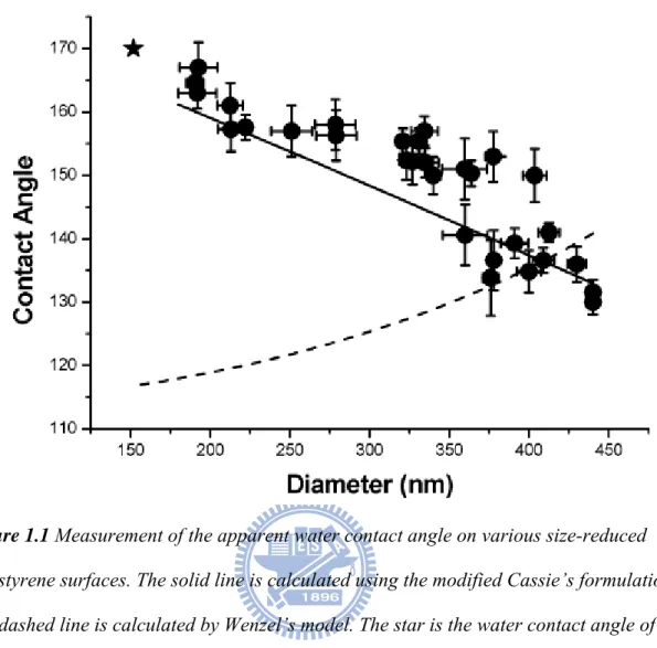
Figure 1.1 Measurement of the apparent water contact angle on various size-reduced polystyrene surfaces. The solid line is calculated using the modified Cassie’s formulation. The dashed line is calculated by Wenzel’s model. The star is the water contact angle of double-layer polystyrene arrays that underwent 120 s of oxygen plasma treatment..………...…...…….4 Figure 1.2 SEM images (60°) of the size-reduced polystyrene beads and the water contact angle measurement on the corresponding modified surfaces (insets). The diameters of polystyrene beads and water contact angles on these surfaces were measured to be (a) 400 nm, 135°, (b) 360 nm, 144°, (c) 330 nm, 152°, and (d) 190 nm, 168°. Bar: 1 µm..………...……..…...……5
Chapter 2 Materials and Experimental Techniques
Figure 2.1 The superhydrophobic micro arrays was formed on substrate after oxygen plasma etching and remove photoresist. (Squre size: 200µm×200µm)……….10 Figure 2.2 Single layer polystyrene beads close-packed in pattern area on silica
substrate.(Size: 400nm).……….…………...…..….11 Figure 2.3 The periodic chromium network on silicon substrate after oxygen plasma
reducing the size of nanoshpere and metal depositing. (Hole size: 200nm).………...12 Figure 2.4 The silicon stamp was made after the dry etching process and removing
chromium layer by CR-7 etchant..……….………….13 Figure 2.5 Polymeric nanostructure obtained by nanoimprint process..……….….14 Figure 2.6 Optical images of water droplet on the roughened fluoropolymer surface before (a) and after (b) applying 300 VAC to the ITO glass.……….………...….14 Figure 2.7 Cross-sectional SEM images of nanoporous structures inside the microchannels.
Bar: 4 µm..………...….16 Figure 2.8 Cell seed on superhydrophobic micro arrays with volume 1000ml.………....16
Chapter 3 Materials and Experimental Techniques
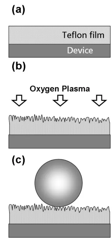
oxygenplasma treatment. (a) The surface of the device is coated with a layer of fluoropolymer (Teflon).(b) Oxygen plasma treatment is used to roughen the surface of fluoropolymer. (c) A superhydrophobicsurface is obtained after the oxygen plasma treatment...….20 Figure 3.2 Schematic for creating a superhydrophobic coating on device surfaces using
nanoimprint process. (a) The silicon substrate is coated with a single layer of well-ordered polystyrene beads. (b) Oxygen plasma is used to reduce the size of polystyrene beads. (c) A layer of chromium is coated on top of the polystyrene beads. (d) Polystyrene beads are then removed by CH2Cl2 solution. (e) The silicon wafer is etched by RIE. (f) The nanoimprint stamp is obtained by removing the chromium layer using CR-7 etchant. (g) The stamp is pressed against the device coated with fluoropolymer. (h) After removing the stamp from the device surface, nanostructure on the surface is obtained...….23 Figure 3.3 SEM images of (a) flat (b) roughened fluoropolymer surfaces. Inset: water
droplets on both surfaces. ...….24 Figure 3.4 Water contact angle measured on the roughened fluoropolymer surface as a
function of oxygen plasma treatment time. ...….25 Figure 3.5 The XPS data of the fluoropolymer coating without oxygen plasma treatment. .
………...………..………26 Figure 3.6 The XPS spectra of a) F (1s), b) C (1s), c) O (1s) peaks for both the flat Teflon
AF (solid line) and the roughened Teflon AF after 10 min of oxygen plasma treatment (dottedline). …………...……….27 Figure 3.7 FTIR spectra of the flat (black) and roughened (red) Teflon AF...……….27 Figure 3.8 SEM images of the nanoimprint stamp created by nanosphere lithography. (a)
Bar: 2 µm; inset bar: 500 nm; (b) bar: 1 µm, the angle of SEM view: 60°.. ….28 Figure 3.9 SEM image of the imprinted nanostructure on the ITO glass surface. Bar: 1.5
µm, the angle of SEM view: 60°. …………...………...…….29
Chapter 4 Observation of Enhanced Cell Adhesion and Transfection Efficiency on the Superhydrophobic Surfaces
Figure 4.1 Patterning process for switchable superhydrophobic surfaces: A) the fluoropolymer was coated on glass substrate. B) A layer of patterned photoresist was used as the mask for the oxygen plasma treatment. C) After
superhydrophobic microarray was obtained by removing the photoresist. E) The cell was cultured on superhydrophobic microarray...….34 Figure 4.2 The AFM images of (a) flat and (b) roughened Teflon AF. Bar: 1 m.
(Measured by VEECO Innova SPM)………..………37 Figure 4.3 The contact angles on the roughened Teflon AF surfaces as a function of
etching time.………...………….………38 Figure 4.4 The surface roughness on the roughened Teflon AF surfaces as a function of
etching time. (Measured by VEECO Innova SPM)………....…………39 Figure 4.5 The fluorescence intensity of the dye conjugated fibronetins on various
surfaces as a function of solution contact time. Open triangles: glass surfaces. Close triangles: PEG presenting surfaces. Open circles: roughened fluoropolymers with a contact angle of 1630. Close circles: flat fluoropolymers.….……….…41 Figure 4.6 The DIC images of (a) NIH 3T3 (b) CHO and (c) HeLa cells on the patterned
superhydrophobic surfaces after 6 hours of incubation. Bar: 200 µm..………...…..43 Figure 4.7 The time-lapse DIC images of NIH 3T3 cells on the patterned
superhydrophobic surfaces after a) 0 minute, b) 50 minutes c) 100 minutes d) 3 hours of incubation. e) After washing the sample with PBS solution. Bar: 200 µm...………...…..44 Figure 4.8 The averaged cell number attached on the roughened fluoropolymer surfaces
as a function of water contact angle. The patterned area is 200µm x 200 µm. The collagen coated glass and flat fluoropolymer were used as controls...45 Figure 4.9 a) Transfection efficiency measured for the CHO cells on the poly D-lysine
(red) and superhydrophobic surface(black). b) The CHO cells on the patterned superhydrophobic surfaces transfected with fluorescence proteins, Kaede. Bar 50 µm. (c) The NIH 3T3 cells on the patterned superhydrophobic surfaces transfected with fluorescence proteins, GFP-actin. Bar 50 µm………...……...46
Chapter 5 Addressable Cell Microarrays by Switchable Superhydrophobic Surfaces Figure 5.1 (a) The switchable superhydrophobic surface is fabricated by roughening a
fibronectin solution is added to the surface and a 150V is applied to the desired electrodes. (c) Fibronectin molecules are deposited to the array with underneath electrode activated. (d) The microarray is then used for cell culture. The cells will only attach to the area coated with fibronectin. (e) The procedure is repeated to culture the second type of cells...53 Figure 5.2 Optical image of an addressable chip containing 4 x 4 switchable
superhydrophobic microarrays...54 Figure 5.3 Fluorescence image of the patterned FITC conjugated anti-chicken IgG
(green) and cy3 conjugated anti-rabbit IgG (red). Bar: 400 µm...55 Figure 5.4 HeLa cells patterned on the switchable superhydrophobic microarrays. Bar:
200 µm...56 Figure 5.5 Fibroblast cells patterned on the switchable superhydrophobic microarrays.
Bar: 200 µm...57 Figure 5.6 Fibroblast cells (red) were first patterned on switchable superhydrophobic
microarray then followed by the HeLa cells (green). Bar: 200 µm...58
Chapter 6 Behavior of single DNA molecules in the well-ordered nanopores
Figure 6.1 Schematic for the fabrication of well-order nanoporous structure in the microchannel using SU-8 photoresist. (a) Silica colloidal crystals are .rst grown inside the SU-8 microchannel. (b) The void spaces of the colloidal crystals are .lled with SU-8 photoresist and cured in the desired area using UV radiation. (c) Inverse opal structures can be obtained after removing the silica nanoparticles with BOE solution and sealing with another layer of SU-8 photoresist. (d) The nanoporous structures are consisted of cavity dc and interconnecting pore dp...64 Figure 6.2 SEM images of nanoporous structures. Silica nanoparticle size (a) 300 nm,
bar: 300 nm; (b) 570 nm, bar: 500 nm...65 Figure 6.3 Sequential images of λ-DNA migrating inside the nanoporous structure
toward the anode at an applied field of 5 V/cm. Elapsed time between frames is 0.1 s. Cavity size: (a) 300 nm, bar: 20µm and (b) 570 nm; bar: 20µm...68 Figure 6.4 (a) Averaged DNA length in two different nanoporous structures. Applied
(average of 500 DNA molecules)... ...69 Figure 6.5 The electrophoretic mobility of (a) λ-DNA and (b) M13mp18 vector as a
function of the applied electric field with two different cavity size of nanoporous structures: 300 nm (black square), 570 nm (open circles) (average of 50 DNA molecules). ...69
Chapter 1 Introduction
Chapter 1
Introduction
1.1 Background
Surface engineering plays an important role in various biological applications, including biosensor technology [1-3] and tissue engineering. [4] In biosensor technology, the ability to create patterns of proteins and cells on the surface is very important, since it is required to monitor living cell behavior when it attach on the surface for studying cell-substrate interaction. Tissue engineering can control the shape of cell adhesion on the surface and the chemistry and topography of the surface where the cell adhered are also important for understanding the relationship between cellular attachment and material surface. Cell adhesion is an important key to biomedical and biotechnological applications. The understanding of the relationship between cell adhesion and substrate are particularly important issue. It has been known that cell attachment contain many proteins including fibronectin, serum albumin and extra cellular matrix (ECM) protein. Therefore, by controlling cell adhesion proteins onto implant surface, the cell attachment behavior is also influenced. For example, if the micro contact printing is used to print fibronectin onto patterned area, the cell can be selected to attach on that area. [5, 6] However, the properties of substrate surface also affect to cell adhesion such as hydrophobicity, surface charge, surface chemistry and roughness. Some reports have shown that cells prefer to grow on surface with specific morphology such as porous and roughness surface. [7] However, there are very limited research activities in exploring the possibility of using the surface morphology as tool for biological applications. We believe that there are many properties
Chapter 1 Introduction
should be discussed between cell-substrate interactions. Especially, by using the materials which can be changed surface morphologic to study cell adhesion.
In this thesis, I describe that use simple approach to prepare polymeric nanostructure arrays with the so-call “superhydrophobic surface”, which can be used to pattern proteins and cells. We also in investigate how the nanostructure affects the surface hydrophobicity and how is it to influence the cell adhesion. Furthermore, the behavior of cell adhesion can be controlled to attach on the selected position of the surface and two different types of cell can be cultured on the same surface.
1.2 Superhydrophobic surfaces
Superhydrophobic surfaces, inspired by the water-repellent behavior of the micro and nanostructured plant surfaces [8, 9], with a water contact angle larger than 150°, have attracted a lot of research attention recently. Because of their unusual large water contact angle, superhydrophobic surfaces can be used as self-cleaning, anti-adhesion, and oxidation-resistant coatings, [10] and it was demonstrated recently that blood cells did not adhere to such type of surfaces [11]. The water-repellent behavior of superhydrophobic surfaces has been explained by two models, [12] the Wenzel and Cassie formulations, which both predict that a nanostructured surface may amplify the surface hydrophobicity as long as a layer of low-surface-energy materials is present on the surface.
In Wenzel’s formulation, it is assumed that the liquid fills up the rough surface, therefore forming a wetted contact, and the apparent water contact angle (θ*) can be written as
cos θ* = λ cos θ,
where λ is the roughness factor which is the ratio of total surface area to the projected area on the horizontal plane and θ is the intrinsic contact angle measured on the flat
Chapter 1 Introduction
rough surface with air trapped below the contact line and the apparent contact angle can be formulated as
cos θ* = Φs (cos θ + 1) - 1,
where Φs is the area fraction of the liquid-solid contact to the projected surface area. In previous work, [12] we have fabricated well-ordered, tunable superhydrophobic surface whose water contact angle can be tuned from 132° to 170° (on a double-layer sample) using a combination of nanosphere lithography and oxygen plasma treatment. The water contact angle on these surfaces can be modeled by the modified Cassie’s formulation without any adjustable parameter (Figure 1.1). The dynamic water contact angle measurement indicates that well-ordered two-dimensional nanostructured systems have relatively large water contact angle hysteresis (Figure 1.2).
It has been suggested that contamination, oxidation, and current conduction can be inhibited on such superhydrophobic surfaces, and the flow resistance in the microfluidic channels can also be reduced using super water-repellent materials. [13] However, to fully utilize the water-repellent properties of the nanostructured surfaces, it is necessary to investigate the relationship between the nanostructure and the water repellent behavior on surfaces and to fabricate the nanostructured surfaces with desired surface hydrophobicity. To fabricate superhydrophobic surfaces, a typical procedure is to create a rough surface covered with low surface energy molecules, such as fluoroalkylsilanes, [14] or to roughen the surface of hydrophobic materials. Several superhydrophobic surfaces have been prepared by these approaches including fluoroalkylsilane-modified inverse opal surfaces, [15] plasma polymerization, [16] anodic oxidation of aluminum, [17] gel-like roughened polypropylene, [18] plasma fluorination of polybutadiene, [19] oxygen plasma-treated poly(tetrefluoroethylene), [20, 21] densely packed aligned carbon nanotubes, [22] aligned
Chapter 1 Introduction
Figure 1.1 Measurement of the apparent water contact angle on various size-reduced polystyrene surfaces. The solid line is calculated using the modified Cassie’s formulation. The dashed line is calculated by Wenzel’s model. The star is the water contact angle of double-layer polystyrene arrays that underwent 120 s of oxygen plasma treatment. [12]
polyacrylonitile nanofibers, [23] and solidification of alkylketene dimmer. [24] A common observation in these experiments is that the water contact angle increases as the surface roughness increases. However, in other experiments [25, 26] it has been demonstrated that smooth well-ordered microstructured surfaces could also produce superhydrophobic surfaces as long as the ratio of the liquid-solid contact area to the overall projected area remains small. It has also been pointed out [27, 28] that the three phase contact line plays a very important role in the contact angle hysteresis, which determines the sliding behavior of water droplets on surfaces.
Chapter 1 Introduction
Figure 1.2 SEM images (60°) of the size-reduced polystyrene beads and the water contact angle measurement on the corresponding modified surfaces (insets). The diameters of polystyrene beads and water contact angles on these surfaces were measured to be (a) 400 nm, 135°, (b) 360 nm, 144°, (c) 330 nm, 152°, and (d) 190 nm, 168°. Bar: 1 µm. [12]
From the above disscution of fabrication procedures, it can be used to prepare superhydrophobic surfaces. However, if the superhydrophobic surfaces are to be used in a microdevice, the modification process should be compatible with the micro-fabrication techniques. For example, if one would like to engineer the surface of a microfluidic device with superhydrophobic properties to reduce the flow resistance, the superhydrophobic material should be integrated into the microfluidic system [17, 29]. Since the surfaces of the microdevices are always flat and smooth, superhydrophobic surfaces can be produced only by roughening a hydrophobic coating. However, almost none of the above-mentioned
Chapter 1 Introduction
techniques can be used directly in such type of applications. Therefore, an alternative approach for producing superhydrophobic coatings on the device surface is needed.
1.3 Aims and Objectives
In this thesis, it has been demonstrated that there are two approaches to impart superhydrophobic properties to the surfaces of micro-devices. First, thin films of a fluoropolymer were spin-coated on the device surfaces followed by an oxygen plasma treatment. However, this approach can not be applied to every hydrophobic materials. In some condition, the surface property will be changed after gas plasma etching. Therefore, the process without changing the chemical properties of polymer should be developed. In the second approach, a nanoimprint process was used to create nanostructures on the polymeric devices. During this process, the polymer only change shape with heating and pressuring when it is filled into imprinting mold. Those two fabrication techniques can be used create superhydrophobic surface on the device which were used to study the adhesion of biological molecule, such as protein and cell. Switchable surface technique is also applied to the superhydrophobic surface to control proteins and cells adhesion by eletrowetting effect.
Another developing of robust three dimensional nanoporous inside microfludic channel will be used to study single DNA molecule behavior. The fabrication is conbined colloidal crystals and micofludic system.
The objectives of this thesis are as follows:
To develop a simple approach to fabricate superhydropohobic micro-devices.
To develop a fabrication nanostructure on polymer without changing its chemical property.
Chapter 1 Introduction
To use eletrowetting effect to control the surface properties. In additional the cell adhesion protein can be patterned on superhydrophobic surface and the cell will attach to the desired position.
To develop three dimensional nanonporous structure inside microfludic system. To use different size of nanostructures to study single DNA behavior with fluoresce
Chapter 2 Materials and Experimental Techniques
Chapter 2
Materials and Experimental
Techniques
A brief review of the materials used and the experimental details that we developed for superhydrophobic micro-device and nanofludic system will be presented. The fabrication include spin-coated, oxygen plasma treatment, nanosphere lithography, nanoimprint, photolithography, microfluidic channel and electrode pattern. In the other hand, the cell was chosen in this experiment including NIH 3T3, CHO and HeLa cell.
2.1 Materials
(1) Poly[tetrafluoroethylene-co-2,2-bis(trifluoromethyl)-4,5-difluoro-
1,3-dioxole] are spin-coated as 5-micron thick film on glass from Teflon AF, DuPont, US.
(2) Indium Tin Oxide (ITO) glass substrate: ITO glass substrates were first patterned by lithograph as a design 200×200 µm square arrays, then cleaned with detergent, and ultrasonicated in acetone and isopropyl alcohol, subsequently dried on hot plate at
Chapter 2 Materials and Experimental Techniques
150 °C for 5 min, and finally treated with oxygen plasma for 5 min. The thickness of ITO is 200 nm.
(3) Polystyrene and Silica nanospheres were chosen by different size from Bangs Laboratories, Inc., Fishers, IN
(4) S1813 is positive photoresist system engineered to satisfy the microelectronics industry’s requirement for advanced IC device fabrication.
(5) SU-8 is a negative, epoxy-type, near-UV photoresist (365 nm) from MicroChem.
2.2 Cell Line
(1) The NIH3T3 is a standard fibroblastcell line, which is a type of cell that synthesizes and maintains the extracellular matrix of many animal tissues.
(2) The CHO cell is a cell line derived from chinese hamster ovary cell.
(3) The HeLa cell is derived from cervical cancer cell, which belong an immortal cell line.
2.3 Experimental Techniques
2.3.1 Preparation of Fluoropolymer Films
The poly[tetrafluoroethylene-co-2,2-bis(trifluoromethyl)-4,5-difluoro-1,3-dioxole] was first spin-coated as 5-micron thick film on glass from Teflon AF, DuPont, US. and heated with hotplate upon 250℃ for 30 minutes to evaporate the solvent.
Chapter 2 Materials and Experimental Techniques
2.3.2 Photolithography and Oxygen Plasma Treatment for
Superhydrophobic Micro Device
A layer of photoresist (S1813, Shipley) was spun on top of the fluoropolymer coating and a photolithographic process was used to define the superhydrophobic area on the photoresist. The superhydrophobic microarray can be manufactured using an oxygen plasma treatment (Oxford Plasmalab 80 Plus, 80W) with a gas O2 (2 sccm) at a total pressure of 25 mTorr. After plasma treatment the photoresist was removed by washing the surface with acetone. Only the areas exposed to the oxygen plasma exhibited the superhydrophobic behavior (Figure 2.1).
Figure 2.1 The superhydrophobic micro arrays was formed on substrate after oxygen plasma etching and remove photoresist. (Squre size: 200µm×200µm)
2.3.3 Nanosphere Lithography
Nanosphere lithography [30-33] is a well-established technique for patterning
large-area periodic nanosphere arrays. By spin-coating the monodisperse polystyrene
beads solution on substrate surfaces, self-organized close-packed nanostructures can be
easily achieved. In this experiment, it has been shown that both single- and double-layer
close-packed polystyrene arrays over a few square centimeter area can be obtained by 200µm
Chapter 2 Materials and Experimental Techniques
adjusting the speed of the spin-coater and the concentration of the surfactants in the
polystyrene solution.A monodispersed polystyrene dispersion with 400 nm diameter beads
(Bangs Laboratories, Inc., Fishers, IN) was used to produce self-assembled close packed
two-dimensional colloidal crystals on a silicon wafer (Figure 2.2).
Figure 2.2 Single layer polystyrene beads close-packed in pattern area on silica substrate.
(Size: 400nm)
2.3.4 Fabrication of Nanostamp in Silicon Base
To prepare silicon nanomold for nanoimprint process, these two-dimensional
colloidal crystals were then used as the template to produce stamps for nanoimprint. To
vary the surface fraction of the nanoimprint stamp, the size of the polystyrene beads was
Chapter 2 Materials and Experimental Techniques
reduced the diameter of the polystyrene beads while keeping their separation distance
unchanged. The diameter of the polystyrene beads could be changed from 400 nm to 200
nm. To fabricate nanoimprint stamp, a 50 nm thick chromium layer was deposited on top
of the trimmed polystyrene beads. Then the polystyrene beads were dissolved in
dichloromethane (Figure 2.3). A dry etching process was used to etch the silicon wafer in
an RIE etcher (Oxford Plasmalab 80 Plus, 110 W, 45 sccm SF6, 5 sccm O2). After the dry
etching process and removing chromium layer by CR-7 etchant, the silicon stamp (30 × 30
mm2) with periodic nanopores was obtained (Figure 2.4).
Figure 2.3 The periodic chromium network on silicon substrate after oxygen plasma
Chapter 2 Materials and Experimental Techniques
Figure 2.4 The silicon stamp was made after the dry etching process and removing
chromium layer by CR-7 etchant.
2.3.5 Nanoimprint
To create a nanostructure on polymer as superhydrophobic microdevice by the
nanoimprint process, a 1 µm thick layer of fluoropolymer was coated on the ITO glass.
Then the nanoimprint stamp was pressed against the polymer coated ITO glass under 70
mbar pressure at 150.C for 30 min. After removing the stamp, nanostructures with desired
dimension can be fabricated on the device surfaces (Figure 2.5).
2.3.6 Switchable Superhydrophobic Surfaces
To fabricate a switchable superhydrophobic surface, electrowettingwas employed to
Chapter 2 Materials and Experimental Techniques
breakdown of the fluoropolymer at high voltage, a layer of silicon oxide (~300 nm) was
deposited on top of the ITO electrode by PECVD before coating the surface with Teflon
AF. To induce a transition from the superhydrophobic state to the completely wetted state,
an AC voltage (300V, 150 Hz) was applied to the ITO glass. The water contact angle on
the roughened fluoropolymer surface could be switched from ~1670 to < 100 as shown in
Figure 2.6
Figure 2.5 Polymeric nanostructure obtained by nanoimprint process.
Figure 2.6 Optical images of water droplet on the roughened fluoropolymer surface before
Chapter 2 Materials and Experimental Techniques
2.3.7 Nanostructure in Microfluidic Channel
To fabricate size-controlled porous nanostructures inside the microfluidic channels, a
cover slip (Technical Glass Product, Painesville Twp, OH) was used as the substrate. A layer of 15 µm thick cured SU-8 photoresist was used as the base layer. A second layer of SU-8 photoresist was then spun on the base layer and then the microchannels were created
in the second layer using a standard photolithography process. The microchannels were
then temporally sealed by conformal contact with a 5 mm think polydimethylsiloxane
(PDMS) slab. Well-ordered colloidal crystals could be grown in the microchannel using
evaporation induced self assembly process. The void spaces in the colloidal crystal were
then filled with SU-8 photoresist. A photomask was used to define the location of the
nanoporous structures inside the microfluidic channel. After dissolving silica colloidal
particles in buffer oxide etch (BOE) solution, well-ordered nanoporous structures inside
the microfluidic system can be obtained (Figure 2.7). These nanoporous structures were
consisted of cavities with a diameter of dc, which represented the size of the original silica
nanoparticles, and interconnecting pores with a diameter of dp. These interconnecting
pores and cavities could be used as the sieving materials for separating biomolecules. The
colloidal particles used in this experiment were 300 nm and 570 nm silica nanoparticles
Chapter 2 Materials and Experimental Techniques
Figure 2.7 Cross-sectional SEM images of nanoporous structures inside the
microchannels. Bar: 4 µm.
2.3.8 Cell Culture on Superhydrophobic Micro Arrays
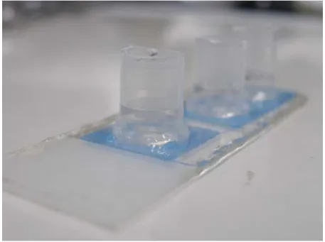
The entire cell was incubated in the chamber with superhydrophobic micro arrays with total volume 1000ml at 37℃ and 5% CO2 in an incubator for 6 hours (Figure 2.8). The concentration of the cell was used 105 cell/c.c. in this process. Then the suspends cell could be removed by PBS washing and taken the DIC image by conforcal microscopy (IX 71, Olympus) for counting the number of the cell on different rough surface.
Chapter 3 Superhydrophobic Coatings for Microdevices
Chapter 3
Superhydrophobic Coatings for
Microdevices
In this chapter, there are two simple techniques to impart superhydrophobic properties to the surfaces of microdevices. In the first approach, thin films of a fluoropolymer were spin-coated on the device surfaces followed by an oxygen plasma treatment. By varying the oxygen plasma treatment time, the water contact angles on device surface could be tuned from 120° to 169°. In the second approach, a nanoimprint process was used to create nanostructures on the devices. To fabricate nanoimprint stamps with various feature sizes, nanosphere lithography was employed to produce a monolayer of
well-ordered close-packed nanoparticle array on the silicon surfaces. After oxygen plasma trimming, metal deposition and dry etching process, silicon stamps with different
Chapter 3 Superhydrophobic Coatings for Microdevices
hydrophobic coatings, such as Teflon, over the device surfaces. The water contact angle as high as 167° was obtained by the second approach.
3.1 Introdution
In the development of modern technology, it is often useful to learn from nature. Many new ideas and inventions have originated from the observation of the behavior of natural materials. One recent example is the so-called “superhydrophobic” materials, which exhibit a water contact angle larger than 150°. Such superhydrophobic materials have lately attracted considerable attention because of their self-cleaning properties. In the past, it was known that a very high water contact angle could be obtained by treating the Teflon surface with oxygen plasma [34, 35]. However, it was only until the discovery of the relationship between the microand nano-structures of the plant surfaces and their water-repellent behavior [36, 37], that researchers started to realize that such superhydrophobic materials might have some important applications. For example, it has been suggested that contamination, oxidation and current conduction can be inhibited on such superhydrophobic surfaces [38], and the flow resistance in the microfluidic channels can also be reduced using the super water-repellent materials [39]. In another example, it was demonstrated that the superhydrophobic surfaces could resist the adhesion of cells and proteins [40]. The self-cleaning and anti-adhesion properties of the superhydrophobic surface could be beneficial to various applications where a clean surface is always required. However, one of the most important issues to incorporate superhydrophobic surfaces into the existing applications is that the surface modification process should be compatible with the current manufacturing techniques, especially the micro-fabrication process.
Chapter 3 Superhydrophobic Coatings for Microdevices
In the past few years, a variety of fabrication procedures have been proposed to prepare superhydrophobic surfaces. In general, superhydrophobic surfaces can be
fabricated by coating a rough surface with low surface energy molecules, such as fluoroalkylsilanes [41] or by roughening the surface of hydrophobic materials. Many superhydrophobic surfaces have been produced by these approaches including fluoroalkylsilane modified inverse opal surfaces [42], plasma polymerization [43], anodic oxidation of aluminum [44], gel-like roughened polypropylene [45], plasma fluorination of polybutadiene [46], oxygen plasma treated poly(tetrafluoroethylene) [34, 47], densely packed aligned carbon nanotubes [48], aligned polyacrylonitile nanofibers [49], and solidification of alkylketene dimmer [50]. If superhydrophobic surfaces are to be used in a microdevice, the modification process should be compatible with the micro-fabrication techniques. For example, if one would like to engineer the surface of a microfluidic device with superhydrophobic properties to reduce the flow resistance, the superhydrophobic material should be integrated into the microfluidic system [39, 51]. Since the surfaces of the microdevices are always flat and smooth, superhydrophobic surfaces can be produced only by roughening a hydrophobic coating. However, almost none of the above-mentioned techniques can be used directly in such type of applications. Therefore, an alternative approach for producing superhydrophobic coatings on the device surface is needed.
Here we describe two simple fabrication processes to modify the surface of the device to achieve a very high water contact angle. In the first approach, the device was first coated with a thin film of hydrophobic materials, fluoropolymer in this case, and then oxygen plasma was used to create superhydrophobic surfaces. However, only in some cases, the chemical properties of the hydrophobic materials could be altered by the oxygen plasma treatment [52]. Therefore, a second technique has been developed where the
Chapter 3 Superhydrophobic Coatings for Microdevices
of these approaches are compatible with the micro-fabrication process.
Figure 3.1 Schematic for producing a superhydrophobic coating on device surfaces using
oxygenplasma treatment. (a) The surface of the device is coated with a layer of
fluoropolymer (Teflon).(b) Oxygen plasma treatment is used to roughen the surface of fluoropolymer. (c) A superhydrophobicsurface is obtained after the oxygen plasma treatment.
Chapter 3 Superhydrophobic Coatings for Microdevices
3.2 Experimental Section
3.2.1 Oxygen Plasma Treatment
One simple approach to create a superhydrophobic surface on a device is to coat the device with a layer of hydrophobic material followed by an oxygen plasma treatment, which roughens the surface of the coating material. The schematic for such process is depicted in Figure 3.1. Since ITO glasses are widely used as the substrates in many industrial applications, such as liquid crystal displays, touch panels, solar cells and microfluidic systems, ITO glasses have been used to mimic
the device surface in these experiments [54–56]. In the first step of this process, a thin layer of fluoropolymer poly [tetrafluoroethylene-co-2,2-bis(trifluoromethyl)- 4,5-difluoro-1,3-dioxole] (Teflon AF, DuPont) was spin coated on the ITO glass at 1000 rpm for 1 min. The thickness of the fluoropolymer was measured to be about 5 µm. The fluoropolymer covered ITO glass was then baked on a hot plate at 150.C for 30 min. After baking, the water contact angle was measured to be 120.. The water contact angle was measured by the sessile drop method where the image of a sessile drop on the sample surface was recorded from its edge through an optical microscope and the contact angle was evaluated from the image by a Dataphysics- SCA20 program. The superhydrophobic surface could be produced by using an oxygen plasma treatment (Oxford Plasmalab 80 Plus, 80W) with O2 gas (20 sccm) at a total pressure of 25 mTorr.
3.2.2 Nanoimprint Process
An alternative approach to fabricate a superhydrophobic surface on a device is to utilize the nanoimprint technique to create nanostructures on the chip surfaces, which are coated with a thin film of hydrophobic materials. The fabrication scheme for a superhydrophobic surface using nanoimprint is illustrated in Figure 3.2 To conduct
Chapter 3 Superhydrophobic Coatings for Microdevices
[57–59], we demonstrated a simple technique to fabricate nanoimprint stamp by nanosphere lithography. In this process, a monodispersed polystyrene dispersion with 400 nm diameter beads (Bangs Laboratories, Inc., Fishers, IN) was used to produce self-assembled close packed two-dimensional colloidal crystals on a silicon wafer. These two-dimensional colloidal crystals were then used as the template to produce stamps for nanoimprint. To vary the surface fraction of the nanoimprint stamp, the size of the polystyrene beads was trimmed by oxygen plasma etching (Oxford Plasmalab 80 Plus, 50 W, 20 sccm O2), which reduced the diameter of the polystyrene beads while keeping their separation distance unchanged. The diameter of the polystyrene beads could be changed from 400 nm to 200 nm. To fabricate nanoimprint stamp, a 50 nm thick chromium layer was deposited on top of the trimmed polystyrene beads. Then the polystyrene beads were dissolved in dichloromethane. A dry etching process was used to etch the silicon wafer in an RIE etcher (Oxford Plasmalab 80 Plus, 110 W, 45 sccm SF6, 5 sccm O2). After the dry etching process and removing chromium layer by CR-7 etchant, the silicon stamp (30 × 30 mm2) with periodic nanopores was obtained.
To create a superhydrophobic surface on the ITO glass by the nanoimprint process, a 1 µm thick layer of polymer (Teflon AF) was coated on the ITO glass. Then the nanoimprint stamp was pressed against the polymer coated ITO glass under 70 mbar pressure at 150.C for 30 min. After removing the stamp, nanostructures with desired dimension can be fabricated on the device surfaces.
3.3 Result and Discussion
3.3.1 Oxygen Plasma Treatment
It has been demonstrated that the oxygen plasma can be used to roughen the surface of Teflon to produce superhydrophobic surfaces [34]. The same concept has been modified in this experiment by using the fluoropolymer coating (Teflon AF), which can be easily
Chapter 3 Superhydrophobic Coatings for Microdevices
Figure 3.2 Schematic for creating a superhydrophobic coating on device surfaces using
nanoimprint process. (a) The silicon substrate is coated with a single layer of well-ordered polystyrene beads. (b) Oxygen plasma is used to reduce the size of polystyrene beads. (c) A layer of chromium is coated on top of the polystyrene beads. (d) Polystyrene beads are then removed by CH2Cl2 solution. (e) The silicon wafer is etched by RIE. (f) The nanoimprint stamp is obtained by removing the chromium layer using CR-7 etchant. (g) The stamp is pressed against the device coated with fluoropolymer. (h) After removing the stamp from the device surface, nanostructure on the surface is obtained.
Chapter 3 Superhydrophobic Coatings for Microdevices
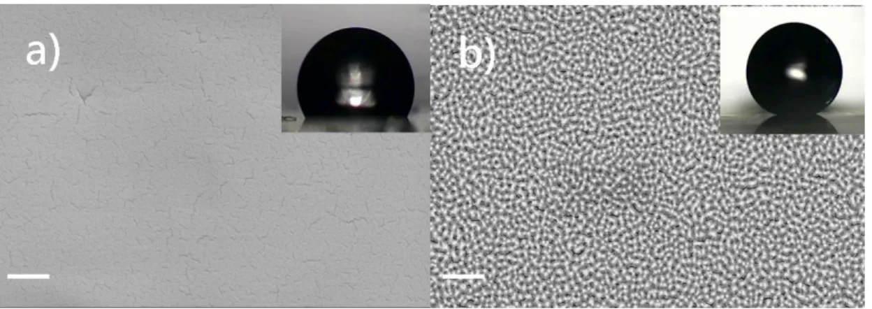
applied to device surfaces. Shown in Figure 3.3 are the SEM images of the fluoropolymer before and after 12 min of oxygen plasma treatment. As a result of oxygen plasma roughening, nanostructures with diameters in the range of 100 nm can be seen from the SEM images. Depending on the time of oxygen plasma treatment, the surface roughness increased from 0.5 nm to 35 nm, whereas
Figure 3.3 SEM images of (a) flat (b) roughened fluoropolymer surfaces. Inset: water
droplets on both surfaces.
the water contact angle on the roughened fluoropolymer surface varied from 120° to 167° as depicted in Figure 3.4. In a word, the hydrophobicity of the surface can be tailored by controlling the oxygen plasma treatment time.
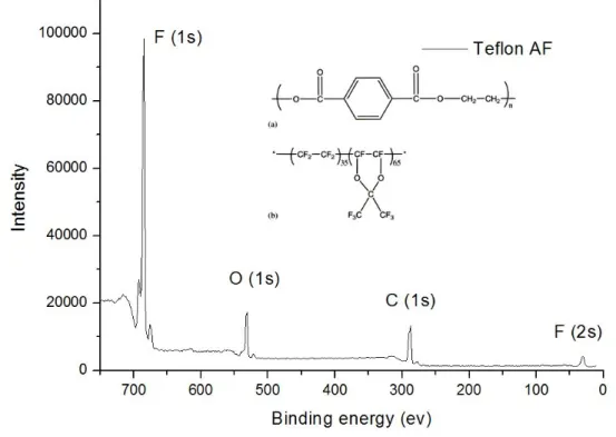
In some applications, it may be desirable to use thin film coatings other than fluoropolymer. However, the oxygen plasma treatment may change the surface chemistry of the coating materials. In the case of Teflon AF, the major effect of oxygen treatment is etching. No significant changes in peak shape and position were observed in the XPS spectra of the fluoropolymer (Figure 3.5) before and after oxygen plasma treatment. And the percentages of the XPS peak areas changed only slightly from 77% (F), 13% (C), 10% (O) for the flat fluoropolymer to 75.6% (F), 12.7% (C), 11.7% (O) for the roughened fluoropolymer (Figure 3.6).
Chapter 3 Superhydrophobic Coatings for Microdevices
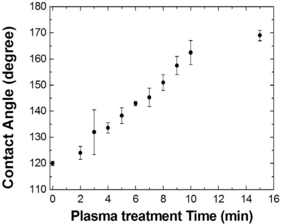
Figure 3.4 Water contact angle measured on the roughened fluoropolymer surface as a
function of oxygen plasma treatment time.
No peak shift or additional peak was observed in the in the FTIR for the roughened fluoropolymer (Figure 3.7). However, if other types of coatings are used, such as SU8 photoresist, poly(dimethylsiloxane) (PDMS) or polyethylene, additional oxygen peaks in the XPS spectra were observed indicating that the surfaces had been chemically modified. In fact, the surfaces of the SU-8 photoresist and PDMS changed from hydrophobic to hydrophilic after the oxygen plasma treatment [52]. Therefore, the oxygen plasma roughening process may not be extended to other types of coatings.
Chapter 3 Superhydrophobic Coatings for Microdevices
Figure 3.5 The XPS data of the fluoropolymer coating without oxygen plasma treatment.
3.3.2 Nanoimprint Process
In a previous experiment, we had utilized nanosphere lithography to create wellordered nanostructures with tunable hydrophobicity on the surface [59]. However, such process is not compatible with micro-fabrication process. We have modified this technique by transferring the pattern of nanostructure into the silicon stamp and the nanostructures can be replicated by nanoimprint process. In other experiments, we had demonstrated that it was possible to create nanoimprint stamp with different dimensions of nanostructures by a combination of nanosphere lithography and oxygen plasma etching [57, 58]. The silicon nanopillar arrays with different shapes and diameters have been obtained by this approach. Following the fabrication process described in the Experimental Section, arrays of nanopores with 200 nm diameter and 300 nm in depth were created as shown in Figure 3.8. To prepare a superhydrophobic coating on the device, the device was first coated with a layer of hydrophobic polymer (Teflon AF in this case). Then the stamp was pressed against the device for 30 min. After removing the stamp, a layer of
Chapter 3 Superhydrophobic Coatings for Microdevices
Figure 3.6 The XPS spectra of a) F (1s), b) C (1s), c) O (1s) peaks for both the flat Teflon AF (solid line) and the roughened Teflon AF after 10 min of oxygen plasma treatment (dotted line).
Chapter 3 Superhydrophobic Coatings for Microdevices
Figure 3.8 SEM images of the nanoimprint stamp created by nanosphere lithography. (a) Dissolve nanosphere after deposit layer of metal(Cr) 50nm, br: 2 µm; inset bar: 500 nm; (b) Silicon nanomold, bar: 1 µm, the angle of SEM view: 60°.
nanostructures on the ITO glass surface. A water contact angle up to 168. was obtained by this approach. Both approaches described here can be used to create superhydrophobic coatings on the device. The advantage of the oxygen plasma is the ease in the fabrication process. However, the oxygen plasma treatment often introduces chemical modification on the surface. For example, the PDMS surface could be changed to hydrophilic after oxygen plasma etching due to the formation of OH. groups on the surface. On the other hand, there is no chemical modification on the surface in the nanoimprint process. Therefore, the nanoimprint process can be extended to all types of hydrophobic coatings.
3.4 Conclusion
In summary, we have developed two techniques to impart superhydrophobic property to the surfaces of devices. In the first approach, oxygen plasma treatment was used to roughen the Teflon coating whose surface water contact angle could betuned form
Chapter 3 Superhydrophobic Coatings for Microdevices
120° to 168° by varying the oxygen plasma treatment time. However, the application of the oxygen plasma process is limited to fluoropolymers. In the second approach,
nanoimprint process was used to create nanostructures on thedevice surfaces where the water contact angle as high as 167° was obtained. In principle, the nanoimprint process can be applied to all types of hydrophobic coatings.
Figure 3.9 SEM image of the imprinted nanostructure on the ITO glass surface. Bar: 1.5 µm, the angle of SEM view: 60°.
Chapter 4 Observation of Enhanced Cell Adhesion and Transfection Efficiency on the
Superhydrophobic Surfaces
Chapter 4
Observation of Enhanced Cell
Adhesion and Transfection Efficiency
on the Superhydrophobic Surfaces
The patterned nanostructure fluropolymer surfaces were used for the study of the cell adhesion. By a combination of photolithography and oxygen plasma treatment, patterned fluropolymer surfaces with various roughnesses have been obtain. The water contact angles measured on the surface were range from 120∘ to 163∘, and surface roughness was measured from 2 nm to 65 nm. When these pattern surfaces were used as the substrates for the cell cultures of HeLa, NIH3T3, and CHO cells, it was found that those cell lines did not adhere to the flat fluropolymer surfaces. However, the number of NIH3T3 and CHO cells adhered on the surfaces increase with the surface roughness. Such nanostructure materials could be used the scaffold for selected cell growth. In conclusion, we report a surprising observation of enhanced cell adhesion and transfection efficiency on the patterned superhydrophobic surfaces, which could be used as cell microarrays.
Chapter 4 Observation of Enhanced Cell Adhesion and Transfection Efficiency on the
Superhydrophobic Surfaces
4.1 Introduction
Ever since the discovery of the importance of the surface roughness to the water repellent behavior of plant leaves, [60] material scientists have developed various strategies [62] to produce the so-called “superhydrophobic surfaces”, whose water contact angles are larger than 1500. It is generally believed that the water repellent properties of the superhydrophobic materials could reduce the water contact area on the surfaces, therefore, minimizing the adsorption of particles or molecules. In the past few years, several potential applications of the superhydrophobic surfaces have been identified including coatings for self-cleaning, fog condensation, contamination reduction, oxidation reduction, oil water separation, and rapid water spreading.[62] However, there are very limited research activities in exploring the possibility of using the superhydrophobic materials for biological applications. The reduced contact area between the solution and surface may minimize the adsorption of biomolecules, therefore, improving the protein resistance on the superhydrophobic surface. It has been shown that the short –term protein resistance on the superhydrophobic surfaces was very similar to the poly (ethylene glycol) (PEG) surfaces, a well-known protein resistance coating, allowing the selective deposition of proteins on the patterned superhydrophobic surfaces. [63] The bioanalytical readout in the protein microarrays fabricated on the superhydrophobic surfaces have been greatly improved owing to the reduced protein adsorption on the superhydrophobic surfaces.[64] It was also shown that the superhydrophobic surfaces could suppress the protein adsorption and promote the flow-induced protein detachment in the microfluidic system.[65] The adhesion of the blood cells was found to be minimized on the superhydrophobic surfaces.[66] Here we report a surprising observation of enhanced cell adhesion and transfection efficiency on the patterned superhydrophobic surfaces, which could be used as cell microarrays.
Chapter 4 Observation of Enhanced Cell Adhesion and Transfection Efficiency on the
Superhydrophobic Surfaces
One of the great challenges in material science is to engineer the surfaces of substrates or devices to regulate the spatial and the temporal behavior of living cells while maintaining their functions.[67] Most of the normal cells need to adhere on the surfaces to proliferate. In vivo, cells are bound to the extracellular matrix (ECM) within tissues. [68] In the cell culture, cells are immobilized to the substrate surfaces through ECM proteins. Therefore, it is very important to investigate the cell-substrate interactions, which is essential to the understanding of biocompatibility, cell culture, cell spreading and tissue engineering. It is recognized that the adhesion of cells on materials depends on the surface characteristics such as wettability, surface charge, surface chemistry, chirality and roughness. [69] Among them, surface wettability is known to be a key factor to the non-specific protein adsorption. It is known that proteins could adsorb rapidly on the hydrophobic surfaces through non-polar interactions while hydrophilic surfaces are less susceptible to the non-specific protein adsorption.[68] Some hydrophilic surfaces, such as PEG modified surfaces, which could bind strongly to the water molecules, have been engineered to resist the protein adsorption. On the other hand, protein adsorption on the hydrophobic surfaces often leads to conformational changes, unfolding or denature of proteins, therefore, permanently contaminating the surfaces. The situation is somewhat different on the superhydrophobic surface. Because the contact between solution and surface is greatly reduced by the surface nanostructures, the protein adsorption was observed to be minimized on such surface for short time.[63] However, as the proteins adsorb on the surface nanostructures, the surface wettability would be changed and the protein adsorption would be accelerated. Since the superhydrophobic surfaces are composed of nanostructures, their surface areas are much larger than the flat surfaces. Therefore, we expect the superhydrophobic surfaces could accumulate more proteins than the flat surfaces of the same materials, if the contact time with the solution is increased.
Chapter 4 Observation of Enhanced Cell Adhesion and Transfection Efficiency on the
Superhydrophobic Surfaces
4.2 Experimental Section
4.2.1 Fabrication of superhydrophobic arrays
To prepare a superhydrophobic surface, the approach was used the same with description of chapter 2, which thin layer of fluoropolymer poly[tetrafluoroethylene-co-2,2-bis(trifluoromethyl)-4,5-difluoro-1,3-dioxole] (Teflon, AF, DuPont) was spin-coated on a cover slip at 3000 rpm for 1 min(Figure 4.1A). The thickness of the fluoropolymer was measured to be about 5 µm. The fluoropolymer coated cover slip was then baked on a hot plate at 1100 for 30 min. After these processes, the water contact angle measured on the fluoropolymer was about 1200. A fluoropolymer surface were then roughened by oxygen plasma treatment (Oxford Plasmalab 80 Plus, 80W) with a gas O2 (2 sccm) at a total pressure of 25 mTorr. The water contact angles on the roughened fluoropolymer surfaces were measured to be 1230, 1350, 1420, 1480, 1580,1630 for 2, 4, 6, 8,10 and 12 minutes of oxygen treatment whereas the surface roughness for these surfaces were 10, 25, 35, 42, 52 nm and 65 nm, respectively. For the cell culture, the chip was designed to have two different roughness states on the same surface (Inside pattern: different rough surface; Outside pattern: flat surface). First, a layer of photoresist (S1813, Shipley) was spun on top of the fluoropolymer and a photolithographic process was used to define the superhydrophobic area (200 × 200 µm) on the photoresist (Figure 4.1B). The superhydrophobic microarray was manufactured using oxygen plasma treatment (Oxford Plasmalab 80 Plus, 80 W) with O2 gas (2 sccm) at a total pressure of 25 mTorr. After plasma treatment the photoresist was removed by washing the surface with acetone. Only the areas exposed to the oxygen plasma exhibited the superhydrophobic behavior (Figure 4.1C and D). For cell incubation, the chip was formed as a chamber which was stuck a plastic tube on the top and the area was about 1 cm (Figure 4.1E).
Chapter 4 Observation of Enhanced Cell Adhesion and Transfection Efficiency on the
Superhydrophobic Surfaces
Figure 4.1 Patterning process for switchable superhydrophobic surfaces: A) the fluoropolymer was coated on glass substrate. B) A layer of patterned photoresist was used as the mask for the oxygen plasma treatment. C) After oxygen plasma treatment, the unprotected area was roughened. D) The superhydrophobic microarray was obtained by removing the photoresist. E) The cell was cultured on superhydrophobic microarray.
Chapter 4 Observation of Enhanced Cell Adhesion and Transfection Efficiency on the
Superhydrophobic Surfaces
4.2.2 Protein absorption with different different surface
To measure the amount of the fibronectin adsorbed on the superhydrophobic surfaces,
roughened fluoropolymers with a water contact angle of 1630 was used in this experiment.
Clean glasses, PEG glasses (Microsurfaces, Inc), and flat fluoropolymers were used as the
control. These substrates were dipped into solution containing 50µg/ml fibronectin
conjugated with Oregon Green (Invitrogen) for a given amount of time and washed by
PBS buffer solution before the fluorescence measurement. The fluorescence of intensity
was measured by a fluoresce microscopy (IX 71, Olympus). All fluorescence intensities
were normalized to the fluorescence intensity measured on a flat glass after 6 hours of
incubation in the fibronectin solution.
4.2.3 Cell Culture on superhrophobic pattern
For the cell adhesion measurement, the patterned superhydrophobic surfaces were
prepared on the cover slips. The detail procedure for preparing the patterned
superhydrophobic surfaces can be found in a previous publication. [63] The dimension for each pattern was 200 µm x 200 µm. Three cell lines, NIH 3T3, CHO and HeLa, were seeded on the patterned superhydrophobic surfaces and placed on a confocal microscope (Fluoview 1000, Olympus) equipped with an incubator (MIU-IBC-IF, Olympus) at 37℃
and 5% CO2 for 6 hours. The density of the cells was about 105 cell/ml. To count the