國
立
交
通
大
學
電機學院 電機與控制學程
碩
士
論
文
降低寄生元件效應的固定導通時間控制於使用陶瓷電
容的降壓電源轉換器
Reduction of Parasitic Component Effect in Constant
On-Time Control for Buck Converter with Multi-layer
Ceramic Capacitors
降低寄生元件效應的固定導通時間控制於使用陶瓷電容的降壓電
源轉換器
Reduction of Parasitic Component Effect in Constant On-Time
Control for Buck Converter with Multi-layer Ceramic Capacitors
研 究 生:徐貴園 Student:Kuei-Yuan Hsu
指導教授:陳科宏 Advisor:Ke-Horng Chen
國 立 交 通 大 學
電機學院 電機與控制學程
碩 士 論 文
A Thesis
Submitted to College of Electrical and Computer Engineering
National Chiao Tung University
in partial Fulfillment of the Requirements
for the Degree of
Master of Science
in
Electrical and Control Engineering
August 2012
Hsinchu, Taiwan, Republic of China
降低寄生元件效應的固定導通時間控制於使用陶瓷電容的降壓電
源轉換器
研究生:徐貴園
指導教授:陳科宏博士
國立交通大學 電機學院 電機與控制學程 碩士班
摘
要
近年來隨著可攜式產品的需求逐漸增加,用來提供可攜式產品系統電源且具有小體 積以及高效能的電壓穩壓器變得越來越重要。實際應用中固定導通時間控制法的電壓穩 壓器常被使用,因為具有幾項優點,如系統結構簡單、快速暫態反應,以及在輕負載時 具有高效率的優點。一般來說,固定導通時間控制法的穩壓器是利用輸出端訊號的漣波 來穩壓,基本上須使用較大等效串聯電阻的輸出電容才可有效控制系統。由於低成本的 優勢,積層陶瓷電容目前被廣泛的使用於消費性電源管理晶片,但是積層陶瓷電容的等 校串聯電阻卻很小。在傳統的控制法使用具有小等效串聯電阻的輸出電容時,由於輸出 端訊號的漣波幾乎僅有電容的成分,故漣波很小系統易受雜訊影響。 因此,本文提出新的固定導通時間控制法電壓穩壓器架構,可提高雜訊容限寬度, 可消除輸出電容上的等效串聯電感及小等效串聯電阻效應。並且由於導通時間可隨輸入 及輸出電壓調整,操作在連續導通模式時的系統切換頻率可以在廣泛的輸入電壓裡維持 幾乎定值。模擬結果顯示出輸出電壓漣波維持約 2 mV,在負載變動範圍為 0 到 600 mA
Reduction of Parasitic Component Effect in Constant On-Time Control for Buck
Converter with Multi-layer Ceramic Capacitors
Student: Kuei-Yuan Hsu Advisor: Dr. Ke-Horng Chen
Degree Program of Electrical and Computer Engineering
National Chiao Tung University
ABSTRACT
In recent years, with the increasing demand of portable products, used to provide system power of portable products with small size and high performance voltage regulator becomes more and more important. Constant on-time control regulators are preferred in practice for several important advantages, such as simple system structure, fast response time and high efficiency for light load. In general, constant on-time control regulators regulate their output voltage based on the ripple component in the output signal. Basically, requires the use of large equivalent series resistance (ESR) of the output capacitance can be effectively controlled system. As a low-cost advantage, multilayer ceramic capacitors (MLCC) are widely used in consumer power management chip, but its equivalent series resistance is very small.
In conventional constant on-time control with small ESR value on the output capacitor, the regulator is easily affected by the noise due to small output ripple, which is dominated by the ripple on the output capacitor.
Therefore, this paper proposes new constant on-time control regulator structure can improve the noise margin, to eliminate the equivalent in series inductance (ESL) and the small equivalent series resistance (ESR) effect. Furthermore, since the on-time period is set simply by input and output voltages, the switching frequency in continuous conduction mode (CCM) operation is relatively constant over a wide input voltage range. Simulation results show that the output ripple keeps around 2mV, when load current step is 600mA and ESR is smaller than 5mΩ.
誌 謝
本論文得以完成,由衷的感謝指導教授 陳科宏博士,這幾年來的辛勤指導與諄諄 教誨,教授平日作學問之嚴謹態度與待人處世之道,更是讓我銘記在心,成為我日後學 習之範典,在此,謹致上最誠摯的敬意及謝意。 感謝立錡科技長官們及同事們的支持,感謝副總戴良彬先生、副總劉景萌先生、副 總張耀輝先生、經理李嘉榮先生是我人生的良師益友感謝長官們的支持。雖然畢業前已 離職,但是長官們支持與體諒銘記在心。 其次,感謝實驗室的學長、學姊的協助與指導。感謝昱輝學長、石頭學長、漢翔學 長與婕妤學姊感謝你們在學業上的指導與協助。 最後,僅將此論文獻給雙親及家人,數十年來父母親勤勞刻苦持家,即便自小我們 是低收入戶的清寒家庭,父母親對我們子女的教育學習更是全力支持及愛護,使我能專 心研究,順利完成學業,在此致上最深的感恩之意。 貴園 于 仲夏 國立交通大學 中華民國一百零一年八月Contents
Chapter 1 ...1
Introduction ...1
1.1 Background of Regulators...1
1.2 Categorization of Power Supply Circuit...2
1.2.1 Linear Regulators ...2 1.2.2 Charge Pump ...4 1.2.3 Switching Regulators...5 1.3 Design Motivation ...9 1.4 Thesis Organization...10 Chapter 2 ... 11
Basic Definition Principles of DC-DC Buck Converters ... 11
2.1 General Specifications... 11
2.1.1 Line Regulation ... 11
2.1.2 Load Regulation ... 11
2.1.3 Transient Response...12
2.2 Losses and Efficiency Analysis ...15
2.2.1 Quiescent Loss...15
2.2.2 Switching Loss ...15
2.2.3 Conduction Loss...16
2.2.4 Efficiency...17
Chapter 3 ...18
Output-Ripple-Based Control of Switching Converter ...18
3.1 Introduction of Output-Ripple-Based Control...18
3.2 Hysteretic Mode Control ...20
3.3 Constant Off-Time Control...22
3.4 Constant On-Time Control ...23
Chapter 4 ...26
Constant On-Time Control with Increase Noise Margin Technology...26
4.1 Conventional Constant On-Time Control Buck Converter ...26
4.1.1 On-Time Control ...29
4.1.2 Analysis Stability Criteria of Constant On-Time Control ...30
4.2 Proposed Constant On-Time Control Buck Structure ...33
Chapter 5 ...37
Circuit Implementation...37
5.1 The Circuit of Increase Noise Margin Technology ...37
Chapter 6 ...40
6.1 Simulation Results...40
6.2 Conclusions ...46
6.3 Future Work ...46
Figure Captions
Fig. 1. Power management system diagram of cell phone. ...2
Fig. 2. The schematic of a low drop-out linear regulator. ...3
Fig. 3. The schematic of a close loop switching capacitor voltage doubler. ...4
Fig. 4. The simple architecture of buck converter. ...5
Fig. 5. The periodic waveform in Fourier analysis...6
Fig. 6. System diagram of buck converter with dynamic load response...13
Fig. 7. Transient waveform of output voltage at load current variation. ...13
Fig. 8. Transient waveform of VDS and ID curve in switching losses on power MOSFET. ...16
Fig. 9. Architecture of the COT control in the DC-DC buck converter. ...18
Fig. 10. The DC-DC buck converter with the hysteretic mode control...20
Fig. 11. The DC-DC buck converter with the hysteretic mode control waveform. ...21
Fig. 12. The DC-DC buck converter with Constant off-time control scheme...22
Fig. 13. The DC-DC buck converter with constant off-time control waveform in DCM. ...22
Fig. 14. The DC-DC buck converter with constant on-time control scheme. ...23
Fig. 15. The DC-DC buck converter with constant on-time control waveform in CCM...24
Fig. 16. The DC-DC buck converter with constant on-time control waveform in DCM...25
Fig. 17. The relationship between the output voltage ripple and the inductor current under different ESR value. ...27
Fig. 18. The ESL effect at the output voltage...28
Fig. 19. On-time control DC-DC buck converter scheme...29
Fig. 20. Small ESR caused double-pulse problem. ...30
Fig. 21. Large ESL caused double-pulse problem...32
Fig. 22. Increase noise margin technology (a) offset voltage applied by switch during the on time. ...34
Fig. 23. Increase noise margin technology (b) offset voltage applied by switch during the minimum off time...34
Fig. 24. Increase noise margin technology (c) offset voltage established by switched current source during the on time. ...35
Fig. 25. Increase noise margin technology (d) offset voltage established by stitched current source during the minimum off time. ...35
Fig. 26. Shows the effect of the switched noise filter and differentiator on the noise margin. 36 Fig. 27. Increase noise margin technology (a) and (b), the VS is pulled up to Vfb + VOS with a switch during the on time or minimum off-time. ...38
Fig. 28. Increase noise margin technology (c) and (d), generates the offset by charging the noise filter capacitor with a switched current source during the on time or minimum off-time. ...39
Fig. 30. Increase noise margin technology (a), Voffset : 10mV , ILOAD=600mA...41
Fig. 31. Increase noise margin technology (c), Voffset : 10mV, no load ...42
Fig. 32. Increase noise margin technology (c), Voffset : 10mV, ILOAD=600mA...42
Fig. 33. Increase noise margin technology (a), Voffset : 10mV , ILOAD=0 to 600mA...44
Fig. 34. Increase noise margin technology (b), Voffset : 10mV , ILOAD=0 to 600mA ...44
Fig. 35. Increase noise margin technology (c), Voffset : 10mV, ILOAD=0 to 600mA ...45
Fig. 36. Increase noise margin technology (d), Voffset : 10mV, ILOAD=0 to 600mA ...45
Table Captions
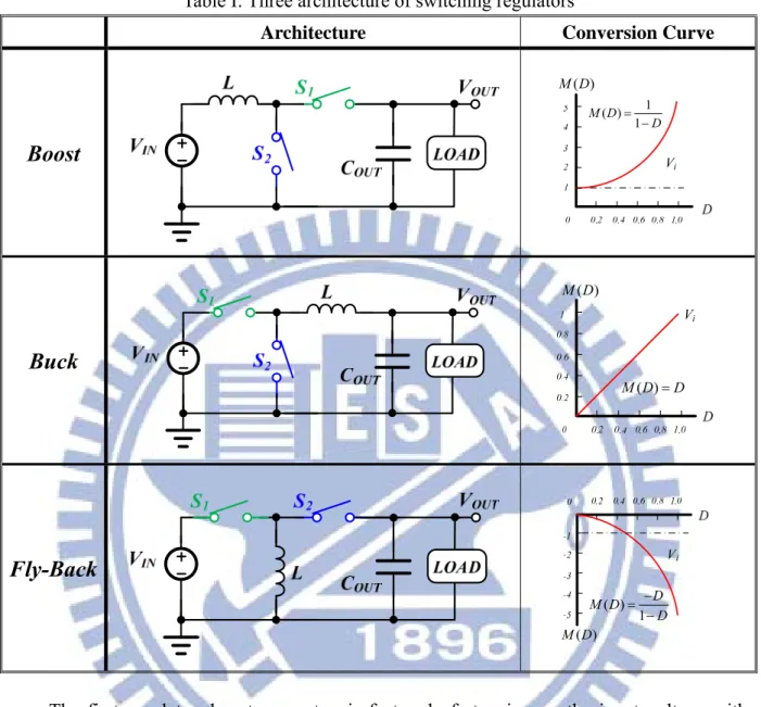
Table I: Three architecture of switching regulators...7Table II: Comparisons of the different power supply circuits. ...8
Table III: Performance of the COT converter...40
Chapter 1
Introduction
1.1 Background of Regulators
In recent years, the portable and battery powered products such as tablet PC, personal digital assistants (PDA), cellular phones, etc., are increasingly demanded more and more. System’s lifetime time is a factor to enhance the worth of the electronic devices in consumer’s market. However, there are many difficulties and limitations to increase the capacity of stored energy device liked as battery equipment. Consequently, power management has become more popular and important subject. That is, how to extend the system operation time and use energy efficiently is a critical issue that engineers mostly concerned.
Furthermore, power management ICs should be essentially designed under the consideration of accomplishing high performance, high-efficiency and low-cost. For meeting these requirements, there are many different kinds of power management architectures could be used, such as buck converter, boost converter, low drop-out (LDO) linear regulator and charge pump, operating with step-up, step-down or inverting voltage. Take cell phone for example, the basic power management system diagram of cell phone is shown in Fig. 1 [1]. The core system includes control unit, processor and many power devices integrated. The control unit can control the state of power device such as sleep, shutdown or active. In this way, we can enhance the operation time and make the power dissipation minimized. This is the reason why the power management system becomes more and more considerable, especially for portable devices.
1.2 Categorization of Power Supply
Circuit
In this section, power management circuits which can classify into three different techniques are introduced including: switching regulators, switching capacitor circuits, and linear regulators. These function and structures are described at the following subsections.
Display
Boost converter Charge pumpRF
circuit
High psrrLDO
Control unit Buck converterDSP core
LCD
panel
LED
driver
Battery
Audio
converterBuckLDO
Interface
converterBuckmanagement IC’s [1].
[2]-[4]. Also, the linear regulator is featured of requires smaller layout area, footprints and simple architecture and low drop-out voltage to provide high efficiency and high performance.
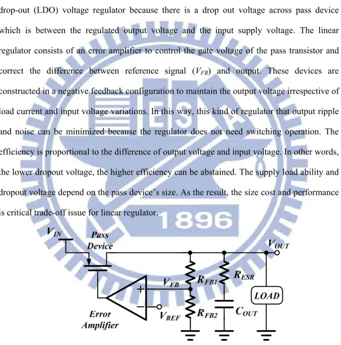
The basic structure of linear regulator is illustrated in Fig. 2. It is also named as low drop-out (LDO) voltage regulator because there is a drop out voltage across pass device which is between the regulated output voltage and the input supply voltage. The linear regulator consists of an error amplifier to control the gate voltage of the pass transistor and correct the difference between reference signal (VFB) and output. These devices are
constructed in a negative feedback configuration to maintain the output voltage irrespective of load current and input voltage variations. In this way, this kind of regulator that output ripple and noise can be minimized because the regulator does not need switching operation. The efficiency is proportional to the difference of output voltage and input voltage. In other words, the lower dropout voltage, the higher efficiency can be abstained. The supply load ability and dropout voltage depend on the pass device’s size. As the result, the size cost and performance is critical trade-off issue for linear regulator.
1.2.2 Charge Pump
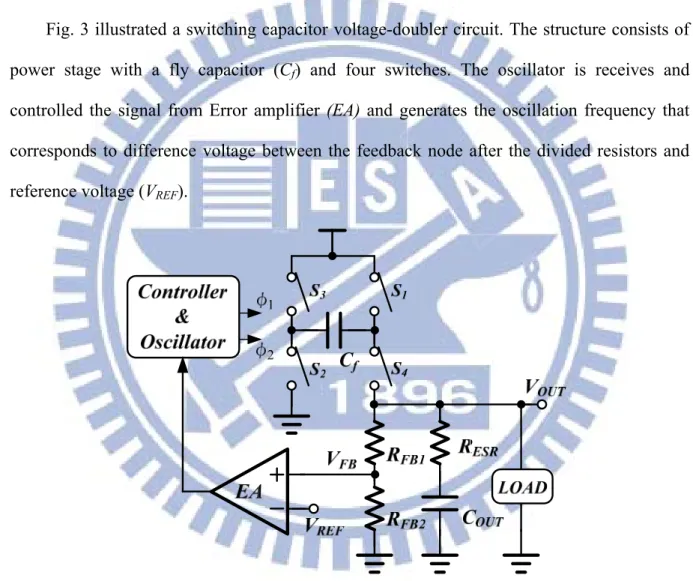
The switching capacitor circuits are usually used to obtain a dc voltage higher or inverting than the supply voltage in low load current applications [5]-[8] and it’s often named as charge pump. The methodology of charge pump circuit is using MOSFET as capacitors and switches as energy storage devices.
Fig. 3 illustrated a switching capacitor voltage-doubler circuit. The structure consists of power stage with a fly capacitor (Cf) and four switches. The oscillator is receives and
controlled the signal from Error amplifier (EA) and generates the oscillation frequency that corresponds to difference voltage between the feedback node after the divided resistors and reference voltage (VREF).
switching S1 and S2 is turned off. The fly capacitor then is connected between VOUT and VIN.
The output voltage equals twice of VIN because of the voltage across fly capacitor is VIN. In
order to maintain the output voltage, there are many ways to modulate the voltage of switching capacitor circuits such as Makowski, Dickson, MPVD, TPVD charge pumps. However, due to digital rail-to-rail switching clock control, the charge pump suffers from output noise problems and EMI.
1.2.3 Switching Regulators
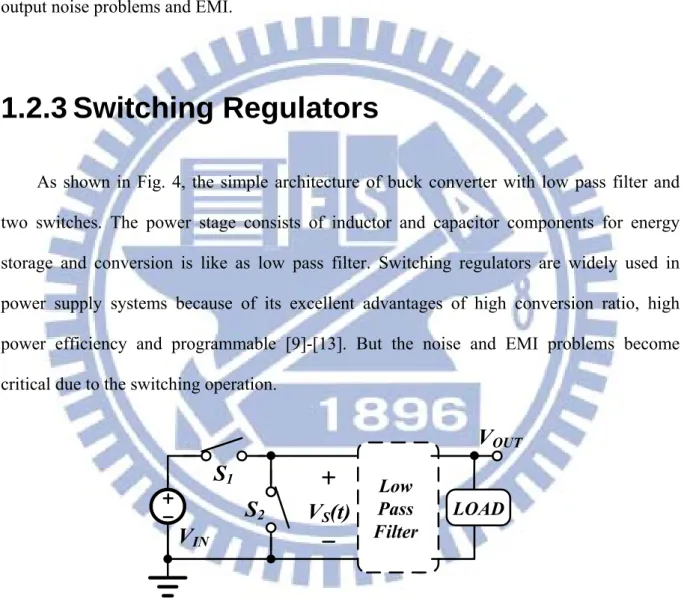
As shown in Fig. 4, the simple architecture of buck converter with low pass filter and two switches. The power stage consists of inductor and capacitor components for energy storage and conversion is like as low pass filter. Switching regulators are widely used in power supply systems because of its excellent advantages of high conversion ratio, high power efficiency and programmable [9]-[13]. But the noise and EMI problems become critical due to the switching operation.
S
1S
2V
IN LOADV
OUT Low Pass FilterV
S(t)
Fig. 4. The simple architecture of buck converter.
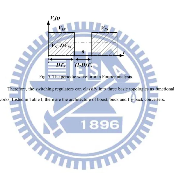
Fig. 5 shows the general form of the pulse signal. When the first phase of S1 closed, the VS(t) equals to the source voltage VIN. In the contrary, when the second phase of S2 closed, the VS(t) equals the ground voltage – zero. Through the low pass filter that consisted with a
value via Fourier analysis. Hence, the dc value of VS(t) is 0
1
( )
s T s s in sV
V t dt DV
T
(1)Therefore, the switching regulators can classify into three basic topologies as functional works. Listed in Table I, there are the architecture of boost, buck and fly-back converters.
V
s(t)
(1-D)T
SV
IN0
V
S=DV
INDT
St
V
INThe first regulator, boost converter, is featured of stepping up the input voltage with respect to output node. The conversion ration M(D) is expressed as M(D)=1/(1-D). The second regulator named as buck converter is featured of stepping down the input voltage with respect to output node. The conversion ration M(D) is expressed as M(D)=D. The last regulator named as fly-back converter also called buck-boost converter is featured of stepping up or down the input voltage with respect to output node. The conversion ratio M(D) is written as M(D)=-D/(1-D).
Linear regulators compared with switching regulator that has advantage of high efficiency because that it constructs by MOSFET as switches and inductor, capacitors as
Table I: Three architecture of switching regulators
Architecture Conversion Curve
Boost
1 ( ) 1 M D D ( ) M DBuck
( ) M D D ( ) M DFly-Back
( ) M D ( ) 1 D M D D energy storage components. When the switch transistor operated in triode region, it’s seen as shot device with little voltage drop across it and it leads to little power dissipation as conduction loss.
On the other hands, there are disadvantages of witching regulator. The control circuit determined time sequence that the structure more complexity than the linear regulators. Also, requirement of discrete components such as capacitors and inductor costs more PCB area. Furthermore, the bandwidth limits the transition response time and the clock signal lead to output noise. These performances are all worse than the linear regulators.
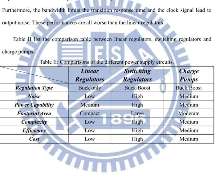
Table II list the comparison table between linear regulators, switching regulators and charge pumps.
Table II: Comparisons of the different power supply circuits.
Linear
Regulators
Switching
Regulators
Charge
Pumps
Regulation Type Buck only Buck/Boost Buck/Boost
Noise Low High Medium
Power Capability Medium High Medium
Footprint Area Compact Large Moderate
Complexity Low High Medium
Efficiency Low High Medium
1.3 Design Motivation
High-quality power supplying converters are demanded for portable devices such as digital cameras, cell phones and other multimedia equipment. That is, efficiency, recovery time, line/load regulation and are treated as important issues in providing a good power supply. Power converter regulates the output voltage as supply voltage and avoids unstable variation in case of load transient which may cause deteriorate or abnormal operation the performance of portable devices.
Switching converters using the output voltage ripple as the PWM ramp signal have been widely used to extend the battery life due to the simple control mechanism [14][15]. Besides, the response time of line and load transient is fast due to large control loop bandwidth. Its control method is usually called ripple-based control [16][17]. Ripple-based control methods include hysteretic control, constant on-time control, and constant off-time control. The hysteretic control is widely used for buck converter to achieve a fast transient response, and the circuitry of the hysteretic control method is compact without complexity. But the major disadvantage of the hysteretic control is the noise effect on the output voltage ripple. This noise can prematurely terminate or initiate a switching period. Another drawback is the switching frequency is affected by parasitic parameters and can change a lot with different input and output voltage.
The constant on-time control operates at a relatively constant frequency without a oscillator due to the on-time period is set by input supply voltage and output voltage, and it does not require error amplifier and loop compensation network, leads to a fast line and load transient response due to its wide control bandwidth. However, the stability is limited with equivalent series resistance (ESR) of output capacitor and output capacitor. If the constant on-time control would be applied in using a low equivalent series resistance of output
capacitor, we must find the ways to compensate the constant on-time control. Especially, with small equivalent series resistance, the output ripple become smaller and the element of equivalent series inductor (ESL) of output capacitor may lead to considerable effect on stability. Consequently, the solution to enhance noise the margin is an important issue to discuss.
1.4 Thesis Organization
The concepts of DC-DC buck converter is organized in chapter 2. The basic ripple-based control of witching converter is introduced in chapter 3. Proposed converter with increase noise margin technology is illustrated in chapter 4. Circuit implementation of the proposed technique is described in chapter 5. Finally, simulation results, conclusion and future work are made in chapter 6.
Chapter 2
Basic Definition Principles of DC-DC
Buck Converters
2.1 General Specifications
There are many specifications and performances of DC-DC converter and required recognition. The following subsections are detail described including significant specifications such as line regulation, load regulation and transient response. Moreover, loss and power efficiency are illustrated.
2.1.1 Line Regulation
Line regulation is a steady-state performance of input voltage variation related to output accuracy. The equation (2) is expressed as below. It can be considered as immunity from input noise. A better line regulation value has more robustness against to supply variation.
Line Regulation OUT ( / )
IN V mV mV V (2)
2.1.2 Load Regulation
It’s the result that estimates the ratio of output voltage variation at different load condition. The equation (3) is expressed as below. That is, when the converter has more immunity from output impedance variation but that has smaller load regulation value.
To get better regulation, the higher system loop gain is required. However, the stability is scarified which is tradeoff between output precision.
Load Regulation
OUT(
/
)
OUT
V
mV mA
I
(3)2.1.3 Transient Response
The transient response is dynamic performance estimated. A good transient response implies that a small voltage variation and faster settling time on output node when output loading changes.
System bandwidth is a one of the factors related transient response. Wide bandwidth implies small voltage drop and faster transient response. It can separate into two fields about time domain and frequency domain analysis.
In frequency domain, literature about [18]-[20], used to position the pole and zero location when transient was occurred. When suffering a load step current variation, it moved the domain pole to higher frequency to get the higher unit gain bandwidth (UGB). In other
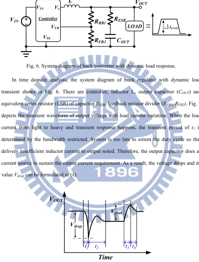
In time domain analysis, the system diagram of buck regulator with dynamic load transient shows in Fig. 6. There are controller, inductor L, output capacitor (COUT) and
equivalent series resistor (ESR) of capacitor RESR, feedback resistor divider (RFB1, RFB2). Fig. 7
depicts the transient waveform of output voltage with load current variation. When the load current from light to heavy and transient response happens, the transient period of t1 is
determined by the bandwidth restricted. System is too late to extent the duty cycle so that delivers insufficient inductor current to output noted. Therefore, the output capacitor does as current source to sustain the output current requirement. As a result, the voltage drops and its value Vdrop can be formulated in (4).
Fig. 7. Transient waveform of output voltage at load current variation. Fig. 6. System diagram of buck converter with dynamic load response.
1 ,
OUT
drop ESR ESR OUT ESR
OUT I t V V V I R C (4)
At this transient period t1, the voltage drop Vdrop equal to the summation of the variation
of charges on capacitor and the VESR. The VESR is the equivalent series resistance of capacitor
and product value of output current variation. The period of t2 is dependent on the time
requirement of the high side transistor to charge the output capacitor to regulated voltage. The summation of t1 and t2 is known as “Recovery Time”. Contrarily, when the load transient is
from heavy to light that will occurs the voltage peak Vpeak of overshoot. When the transient
response occurs, the t3 is transient period with too much current which is supplied from high
side transistor. The system is too late to reduce the duty cycle that decrease inductor current into output node and the system bandwidth also restricted the speed of feedback response. As a result, the output goes toward high and overshoot Vpeak is formulated as below.
At this transient period, the Vpeak equals to the summation of variation of charges on
capacitor and the VESR. During the period t4, the redundant energy on output capacitor is
consumed from light load and discharged through feedback resistor. As the result, the output voltage goes back to regulated level gradually.
3
,
OUT
peak ESR ESR OUT ESR
OUT
I
t
V
V
V
I
R
C
(5)2.2 Losses and Efficiency Analysis
Power loss of switching regulators is the combination of the switching loss and the MOSFET’s conduction loss as shown in equation (6). The power loss is important factor to determine efficiency and it is briefly introduced as following.
2.2.1 Quiescent Loss
The quiescent loss also called as static loss that was consumed by other controllers of switching regulators. The smaller quiescent loss also causes higher efficiency.
Q IN Q
P
V
I
(7)The other power losses that don’t be mentioned above obeyed the rules ofI R . 2
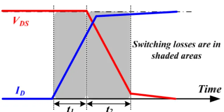
2.2.2 Switching Loss
The switching interval begins when the high-side MOSFET driver turns on and begins to supply current power MOSFET’s gate to charge its input capacitance. The switching loss is involved of the charge on the parasitic capacitor of switching node. Therefore, there is no switching loss until VGS reaches the low-side MOSFET’s VTH.
MOSFET SW COND
When VGS reaches VTH, the input capacitance of gate is being charged and the MOSFET’s
drain current ID is rising up linearly until it reaches the current IL which is presumed to be ILOAD. During this period (t1) the MOSFET is sustaining the entire input voltage VIN across it,
the energy in MOSFET during t1 is:
1 1
(
2
)
IN LOAD t
V
I
P
t
(8)Sequentially, as the beginning time of second period t2, the current flowing through
high-side MOSFET is ILOAD, and the VDS begins to fall. All of the gate current will be going to
recharge CGD. CGD is similar to the “Miller” capacitance of transistor, so t2 could be thought of
as “Miller time”. During this time the current is constant as ILOAD and the voltage is falling
fairly linearly from VIN to 0, therefore:
2 2
(
2
)
IN OUT t
V
I
P
t
(9)The total switching loss for any given edge is just the power that occurs in each switching interval, multiplied by the duty cycle of the switching interval:
loss. High-side conduction loss is calculated straightforward that is just the I R loss timing 2
the MOSFET’s duty cycle as below:
Where RDS ON( ) is at the maximum equivalent resistor on operation MOSFET. In the same way, low-side conduction loss is determined as (12).
2.2.4 Efficiency
The efficiency of switching regulator is defined as the ratio of the output power consumption and input power supplies, which is formed as below equation (13):
100%
OUT OUT ff IN O SW COND Q ElseP
P
E
P
P
P
P
P
P
(13)The total power consumption of input power supplies is involved of the output consumption (PO), switching loss (PSW), conduction loss (PCOND), quiescent loss (PQ), and
other losses (PElse) in parasitic elements. A high efficiency results in a high performance
extending the battery life.
2 ( ) OUT COND OUT DS ON IN V P I R V (11) 2 ( ) (1 OUT) COND OUT DS ON IN V P I R V (12)
Chapter 3
Output-Ripple-Based Control of
Switching Converter
3.1 Introduction of
Output-Ripple-Based Control
The output-ripple-based control commonly refers to the DC-DC converters that use the output ripple voltage as pulse width modulation (PWM) information. Fig. 9 shows a general DC-DC buck converter block diagram with the output-ripple-based control. The output state of feedback voltage VFB compares with the reference VREF signal to determine the operation of
according to the output load without the need of additional complex frequency tuner. That is, the convertor acts as variable frequency modulation (VFM) and saves significantly switching loss to maintain good efficiency at light loads for portable power electronics. Consequently, the output-ripple-based control becomes one considerable choice among many power management designs.
The advantages of the constant on-time control can be summarized as follows. (a) Self-oscillating without any oscillators.
(b) Simple structure without error amplifier. (c) High efficiency at light load.
(d) Fast transient response.
However, the practical problems and limitations are suffered from as follows. (a) Jitter behavior due to low noise immunity.
(b) EMI issue because of poorly defined switching frequency.
(c) Sub-harmonic instability due to inappropriate output capacitor application. (d) Inadequate DC regulation due to the nonlinear loop control.
Three kinds of basic output-ripple-based control method of buck converter including hysteretic control, constant off-time control and constant on-time control are introduced in the following.
3.2 Hysteretic Mode Control
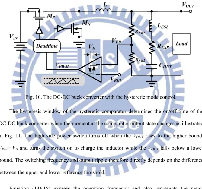
The architecture of the hysteretic mode control is shown in Fig. 10. This control methodology make the output oscillate within a predefined error band called hysteresis band or hysteresis window (VH).
Fig. 10. The DC-DC buck converter with the hysteretic mode control.
The hysteresis window of the hysteretic comparator determines the on/off time of the DC-DC buck converter when the moment at the comparator output state changes as illustrated in Fig. 11. The high side power switch turns off when the VOUT rises to the higher bound,
VREF+VH and turns the switch on to charge the inductor while the VOUT falls below a lower
bound. The switching frequency and output ripple therefore directly depends on the difference between the upper and lower reference threshold.
( )
( - )
ESR IN OUT OUT SW H eff IN R V V V f V L V (14) ESR OUT ON ESR OUT IN OFF IN ESL FB FB H eff H R L V T R L V V T V L L R R V V (1 ) 1 2 ) ( (15)
But the hysteresis controllers are still favored in audio applications owing to their high linearity and simple design.
3.3 Constant Off-Time Control
The approach of constant off-time control is similar to constant on-time control as illustrating in Fig. 12. In normal operation, the system initiates an off-time period when the feedback voltage VFB rises above the reference voltage VREF. Also, this control technique is
called “peak control”.
L
V
OUTR
ESRC
OUTL
ESL LoadV
INV
REF COMPV
FB RFB1 RFB2M
NM
P Deadtime MMV Q QHowever, constant on-time control is more popular than constant off-time control in application of power management system. The reason is that the switching frequency in DCM operation of constant off-time control is inversely proportional to the load current (i.e., the switching loss is considerable and deteriorates to poor efficiency.). Waveform shown in Fig. 13 is the constant off-time control operating in DCM.
3.4 Constant On-Time Control
As shown in Fig. 14, the basic constant on-time control structure consists of a comparator and mono-stable multi-vibrator (MMV), with the output voltage feedback compared with an internal reference. MMV is a circuit to generate a constant on-time and to adjust adaptively itself to variable using condition such as input supply voltage and output voltage. The constant on-time control method is a modification of hysteretic control that operates at a relative constant frequency without an oscillator.
L
V
OUTR
ESRC
OUTL
ESL LoadV
INV
REF COMPV
FB RFB1 RFB2M
NM
P Deadtime MMV Q QFig. 14. The DC-DC buck converter with constant on-time control scheme.
When the feedback voltage VFB falls below the reference voltage VREF initiated on-time
switch stays on for the programmed on-time (TON), causing the feedback voltage to rise above
the reference voltage. After the on-time period, the power switch remains off until the feedback voltage falls below the reference voltage and repeats the cycle again and again. The switching frequency as equation (16) of constant on-time in control continuous conduction mode (CCM) is easier to define than hysteretic mode control.
V
PWM VREFI
LOADt
TOFF TONV
FBFig. 15. The DC-DC buck converter with constant on-time control waveform in CCM. Equation (16) shows the switching frequency is only related the output voltage, TON and
input voltage. TON can be designed to compensate the variation and will discuss in Chapter 4. OUT SW IN ON
V
f
V T
(16)In the contrary, while in discontinuous conduction mode (DCM) experienced at light loads, the frequency will vary according to the load condition, similar to the operation in PFM mode [25]. This leads to good transient response and high efficiency.
from charging at one on-time period. In other words, switching frequency of constant on-time control is dependent on load current condition in DCM operation.
Chapter 4
Constant On-Time Control with
Increase Noise Margin Technology
4.1 Conventional Constant On-Time
Control Buck Converter
The basic concept of constant on-time control is introduced in chapter 3. Besides, constant on-time control is more popular than constant off-time control owing to the conversion efficiency at light loads. In this section, we will describe the on-time control and analyze the system stability of constant on-time control in time-domain and frequency-domain, respectively.
As shown in Fig. 17, the output voltage ripple caused by the inductor current ripple contains three major terms, which are VESL, VESR, and VCOUT due to the parasitic effect on the
output capacitor COUT. The VESR and the VESL are represented the voltage ripples cause by the
equivalent series resistance (ESR) and the equivalent series inductance (ESL). The VCOUT is
(MLCC) will be excluded due to its low ESR. However, the MLCC is one of the suitable choices owing to it low cost [22][23][24]. Thus, it becomes one important issue to overcome this problem. In this paper, increase noise margin technology is proposed to ensure the stability when the MLCC is utilized.
VESL VCOUT Vref Mediu m RESR Large RESR Small RESR Vref Vref VOUT VOUT VOUT ILoad IL t t t t t t Component of VOUT VESR
~
~
Fig. 17. The relationship between the output voltage ripple and the inductor current under different ESR value.
Another factor affecting the stability of the factors, equivalent series inductance (ESL).The ESL will distort the feedback control signal VFB by the voltage step, VESL, as shown
in (17) and (18). It results in the on-time timer might be trigger at the incorrect time. As depicted in Fig. 18, the VESL is proportional to the VIN and the LESL. It will discuss in Chapter
4.1.2.
in
ESL ESL p ESL n ESL
V
v
v
v
L
L
(17)where
in outand
outESL p ESL ESL n ESL
V
V
V
v
L
v
L
L
L
(18)4.1.1 On-Time Control
For maintaining the switching frequency constant, the adaptive on-time circuit adjusts the on-time period according to output voltage VOUT and supply voltage VIN, as shown in Fig.
19.
Fig. 19. On-time control DC-DC buck converter scheme.
As the above mentioning, the switching frequency is determined by (16). If the on-time (TON) is directly proportional to output voltage and inversely proportional to input voltage
(19), then its switching frequency will be pseudo fixed frequency (20).
Constant
OUT ON INV
T
V
(19) ( )Constant
Constant
OUT SW NEW OUT IN INV
f
V
V
V
(20)4.1.2 Analysis Stability Criteria of Constant
On-Time Control
In conventional constant on-time control with small ESR value on the output capacitor, the converter is easily affected by the noise due to small output ripple, which is dominated by the ripple on the output capacitor. Besides, the loop phase delay may further decrease the system stability owing to the double-pulse problem. As illustrated in Fig. 20, the delayed output voltage, VOUT, is unable to reach the reference voltage, Vref, even after the first constant
on-time period. Consequently, the second constant on-time is inserted after the minimum off-time period to raise VOUT higher than Vref. The constant on-time control can’t regulate the
output voltage within one switching cycle and thus induces the double-pulse problem. That is, the system needs two or more switching periods to regulate the output voltage. The output voltage ripple is increased to ensure the system stability due to the decreased switching frequency.
L V V dt dI m L IN OUT (21) L V m' OUT (22) The value of VOUTfor time=t can be calculated as shown in (23). RESR is the ESR on
output capacitor. LESLis the ESL on the output capacitor. ΔILis the inductor current variation
during one on-time period.
1 ( ) ' ) ( I mt dt L m C mt R V t V L ESL O ESR ref OUT (23)The output ripple is composed of three components including ESR part, capacitor part and ESL part. In (23), the second term indicates the contribution of the ESR while the third term represents the ripple on the output capacitor. The last term indicates the contribution of the ESL. To ensure the system can be regulated for each switching cycle. At t=TON, the value
of VOUT (TON) needs to be larger than Vref as shown in (24).
0 2 ) ( 2 2 L m' C mT C mT mT R V T V ESL O ON O ON ON ESR ref ON OUT (24)
The arrangement of (24) can be expressed in (25). 2 ON OUT IN OUT ON O ESL O ESR T V V V T C L C R (25)
That is, the time constant, RESRCO, must be larger than half of on-time period to ensure
the system stability. Consequently, the ripple contributed by the ESR dominates the whole output ripple to guarantee the system stability. Therefore, a large ESR is utilized in the conventional constant on-time control at the sacrifice of large output ripple. However, for certain applications of output capacitor combination, as the total ESL of the output capacitor becomes larger, the double-pulse problem will appear as shown in Fig. 21. At the beginning of the minimum off-time, the voltage across ESL will step down since the negative slope of inductor current. If the voltage spike on the ESL is larger enough to let the output voltage smaller than Vref, the second constant on-time period will appear. Large ESL will cause the
4.2 Proposed Constant On-Time
Control Buck Structure
The concept of the switched noise filter is to add a small offset to the capacitor voltage in each switching period. From the Fig. 22 to the Fig. 25, shows the proposed constant on-time control DC-DC converter with increase noise margin technology.
In the circuit of Fig. 22 (a constant on-time buck converter with valley control), the feedback voltage through the differentiator generates a differential signal. And during the on time the VS is pulled up to Vref + VOS with a switch. Fig. 23 shows the same circuit, but here
the VS is pulled up to Vref + VOS during the minimum off time. Fig. 24 and Fig. 25 show a
different method of establishing the offset in the same converter. The circuit in Fig. 24 generates the offset by charging the noise filter capacitor with a switched current source during the on time. The circuit in Fig. 25 generates the offset by charging the noise filter capacitor during the minimum off time. The above methods can be easily modified for use in constant on-time control buck converter.
C
OR
FB1R
FB2L
V
outLX
SW
NSW
PV
inR
esr S R Q Loop ComparatorL
esl Logic ZCD Deadtime Control On-Time TimerV
fb Minimum Off-Time TimerV
zcdV
offV
resetV
SWPV
clrV
refC
NFV
OS DifferentiatorV
sFig. 22. Increase noise margin technology (a) offset voltage applied by switch during the on time.
C
OR
FB1R
FB2L
LX
SW
NSW
PV
inR
esr S R Q Loop ComparatorL
esl Logic ZCD Deadtime Control On-Time TimerV
fb Minimum Off-Time TimerV
zcdV
offV
resetV
SWPV
clrV
refC
NF DifferentiatorI
OSV
outV
sFig. 24. Increase noise margin technology (c) offset voltage established by switched current source during the on time.
C
OR
FB1R
FB2L
LX
SW
NSW
PV
inR
esr S R Q Loop ComparatorL
esl Logic ZCD Deadtime Control On-Time TimerV
fb Minimum Off-Time TimerV
zcdV
offV
resetV
SWPV
clrV
refC
NF DifferentiatorI
OSV
outV
sFig. 25. Increase noise margin technology (d) offset voltage established by stitched current source during the minimum off time.
The proposed increase noise margin technology is the Vfb through the differentiator
During the on time or minimum off time the noise filter capacitor is charged up to Vref + VOS with a switch. The signal (VS) to get the inductor current information and it can be viewed
as a ramp signal, providing good noise immunity for system operation. As the Fig. 26, it shows the effect of the switched noise filter and differentiator on the noise margin.
Chapter 5
Circuit Implementation
5.1 The Circuit of Increase Noise
Margin Technology
The proposed structure is depicted in Fig. 27 and Fig. 28. The differentiator is composed of M1-M9, C1-C2, and OP1. Differentiating feedback voltage Vfb through the capacitor C1, the
inductor current can be derived. Vd is composed of ESR and inductor current ripple
information. However, Vd has unwilling distortion due to equivalent series inductor effect of
output capacitor. The expressions of Vfb and Vd are shown in (26) and (27), respectively.
dt dI L dt I C I R k V L ESL L O L ESR fb 1 (26) 2 2 ' dt I d L C I L V V R k V V ESL L O L OUT IN ESR d d
(27)The k is the feedback ratio and τ is a constant generated in the procedure of differentiation. The unwilling ESL effect caused by LESL is a high frequency component,
which will result in a surge on the differential voltage Vd. To avoid this problem, a capacitor C2 is introduced at the gates of transistors M6 and M7. Therefore, the current IL flowing into M7 is filtered by C2. That is, the high frequency component of Vd has been eliminated. Then,
the equivalent series inductor effect can be reduced. After that, the current IH flowing into M8
is mirrored to M9, and IH is the deduction of IHL about IL. That is, IH contains high frequency
from IHL. The voltage V2 would therefore contain low frequency component only, eliminating
the equivalent series inductor effect of output capacitor. And for power supply rejection that add the cascode circuit (Ma-Md).
The current mirror circuit is composed of M13-M15, R3, R4 and OP3. The V3 is
proportional to enlarge the V2 signal it's for common-mode feedback circuits (CMFB) input
node. The CMFB circuit is composed of M16-M18, R5 and OP4, the input nodes are V3 and VS.
And the V4 is feedback node that adjusts the VS voltage for convergence differences between
the corners. The VS is not only proportional to enlarge by V2 but also is controlled by CMFB
feedback node, and compare with feedback voltage Vfb. The proportional to enlarge circuit is
composed of M10- M12, R1, R2 and OP2. Besides, the offset voltage is provided by the voltage
source is not generated by the current source. The current mirror circuit is composed of
M19-M21, R5 and OP5. It is proportional to narrow the Vadd signal and add the voltage to VS
Basically, most of the circuit structures of Fig. 28 the same with Fig. 27. But, the generate the offset voltage by charging the noise filter capacitor with a current source (IB2),
and the current source control by MI during the on time or minimum off-time.
Fig. 28. Increase noise margin technology (c) and (d), generates the offset by charging the noise filter capacitor with a switched current source during the on time or minimum off-time.
Chapter 6
Simulation Results, Conclusions and
Future Work
6.1 Simulation Results
The specifications of the proposed converter are listed in Table III. Table III: Performance of the COT converter
Process UMC 0.25μm
Supply voltage (VIN) 3.3V
Output voltage(VOUT) 1.8V
Load range (ILOAD) 0mA – 600mA
Inductor 4.7 μH
Output Capacitor 10 μF MLCC
RESR 5mΩ
LESL 2nH
Operation frequency (CCM) 1.5MHz
Output ripple @ ILOAD=600mA 2mV
From the Fig. 29 to Fig. 32 shows the steady-state of simulation results at different load current condition when the converter operates in the DCM and CCM. Fig. 29 and Fig. 31 are
2mV. Furthermore, the switching frequency reduces for power saving when the load current decrease in the DCM.
Fig. 29. Increase noise margin technology (a), Voffset : 10mV, no load
Fig. 30. Increase noise margin technology (a), Voffset : 10mV , ILOAD=600mA
VOUT VS VFB Driver ΔVOUT = 2mV Noise margin = 10mV VOUT VS VFB Driver ΔVOUT = 2mV Noise margin = 10mV
Fig. 31. Increase noise margin technology (c), Voffset : 10mV, no load VOUT VS VFB Driver ΔVOUT = 2mV Noise margin = 10mV VOUT VS VFB Driver ΔVOUT = 2mV Noise margin = 10mV
From the Fig. 33 to Fig. 36 shows the load transient response of simulation results when the converter operates from DCM to CCM. The increase noise margin technology provides good noise margin for constant on-time control system to operate correctly with low ESR exist at output capacitor. But in increase noise margin technology (b) and (d), if the offset voltage is not big enough system will become unstable.
The simulation result is as the table IV. The increase noise margin technology provides the stable output, but it’s got larger load regulation. The circuit adds the increase noise margin technology or not, that is trade-off between stability and Load regulation.
Table IV: Simulation Result Table
No Load ILOAD = 600mA
Simulation item (a) VOUT-RIPPLE = 2mV output voltage stable
VOUT = 1.477V
VOUT-RIPPLE = 2mV output voltage stable
VOUT = 1.405V Simulation item (b) Unstable
TMIN-OFF is too short noise margin too small
VOUT = 1.52V
Unstable TMIN-OFF is too short noise margin too small
VOUT = 1.46V Simulation item (c) VOUT-RIPPLE = 2mV
output voltage stable VOUT = 1.729V
VOUT-RIPPLE = 2mV output voltage stable
VOUT = 1.605V Simulation item (d) Unstable
TMIN-OFF is too short noise margin too small
VOUT = 1.76V
Unstable TMIN-OFF is too short noise margin too small
Fig. 33. Increase noise margin technology (a), Voffset : 10mV , ILOAD=0 to 600mA VOUT VS VFB Driver VOUT VS VFB Driver
Fig. 35. Increase noise margin technology (c), Voffset : 10mV, ILOAD=0 to 600mA
Fig. 36. Increase noise margin technology (d), Voffset : 10mV, ILOAD=0 to 600mA
VOUT VS VFB Driver VOUT VS VFB Driver
6.2 Conclusions
The noise margin technique is proposed in this thesis to eliminate equivalent series inductor (ESL) and equivalent series resistor (ESR) effect and and remove the dependency of output ripple induced by ESR in constant on-time control DC-DC converter of output capacitor. The noise margin technique is add the offset voltage during the on time or minimum off time is proposed structure for constant on-time control DC-DC buck converter. Because the noise margin at the comparator input node has been increased, so it can avoid the noise. The system can operate correctly even that very small ESR exists at output capacitor both in CCM and DCM.
6.3 Future Work
This thesis proposes a solution for constant on-time control DC-DC buck converter with using MLCC as output capacitor. The proposed increase noise margin technology not only removes the small ESR issue but also aims to eliminate ESL effect of the output capacitor. But, the output voltage DC level is not accurately defined. Because, that the magnitude of the offset voltage will affect the output voltage accuracy. There can add the cancel the offset voltage effect technique from Vref. Finally, the experimental result should be presented to
Reference
[1] D. Maksimovic, “Power management model and implementation of power management ICs for next generation wireless applications,” Tutorial presented at the International
Conference on Circuits and System (ISCAS), 2002.
[2] Hong-Wei Huang, Chia-Hsiang Lin, and Ke-Horng Chen, “Low-Dropout Regulators with Adaptive Reference Control and Dynamic Push-Pull Techniques for Enhancing Transient Performance,” the 34th European Solid-State Circuits Conference (ESSCIRC),
Sep. 2008.
[3] Huan-JenYang, Han-Hsiang Huang, Chi-Lin Chen, Ming-Hsin Huang, and Ke-Horng Chen, “Current Feedback Compensation (CFC) Technique for Adaptively Adjusting the Phase Margin in Capacitor-Free LDO Regulators,” 51th IEEE Int'l Midwest Symposium
on Circuits & Systems, Aug. 2008.
[4] Yung-Hsin Lin, Kuo-Lin Zheng, and Ke-Horng Chen, “Power MOSFET Array for Smooth Pole Tracking in LDO Regulator Compensation,” 50th IEEE Int'l Midwest
Symposium on Circuits & Systems/5th IEEE Int'l Northeast Workshop on Circuits & Systems, pp. 554-557, Aug. 2007.
[5] P. Favrat, P. Deval and M. J. Declercq, ”A high-efficiency CMOS voltage doubler,”
IEEE Journal of Solid-State Circuits, vol. 33, pp. 410-416, March 1998.
[6] Starzyk, J.A, Ying-Wei Jan and Fengjing Qiu, “A DC-DC charge pump design based on voltage doublers,” IEEE Trans. Circuits and Systems I, vol. 48, pp. 350-359, Mar. 2001. [7] Chun-Yu Hsieh, Po-Chin Fan and Ke-Horng Chen, “A Dual Phase Charge Pump with
Compact Size,” the 14th IEEE International Conference on Electronics, Circuits and
Systems, pp.202-205, Dec., 2007.
Regulator with Nano-Ampere Switched-Capacitor CMOS Voltage Reference for Achieving Low Output Ripples,”the 15th IEEE International Conference on Electronics, Circuits and Systems, Sep., 2008.
[9] Cheung Fai Lee, Philip K. T. “A Monolithic Current-Mode CMOS DC-DC Converter with On-Chip Current-Sensing Technique,”. IEEE J. Solid-State Circuits. vol. 39, pp.3-13, Jan. 2004.
[10] Chi Yat Leung, Philip K.T. Mok, “A 1-V Integrated Current-Mode Boost Converter in Standard 3.3/5-V CMOS Technologies,” IEEE Journal of Solid-State Circuits, vol. 40, no. 11, Nov. 2005.
[11] Ming-Hsin Huang, Ke-Horng Chen, and Wei-Hsin Wei “Single-Inductor Dual-Output DC-DC Converters with High Light-Load Efficiency and Minimized Cross-Regulation for Portable Devices,” IEEE VLSI-Symposium on Technology and Circuits, June, 2008. [12] Hong-Wei Huang, Hsin-Hsin Ho, Chieh-Ching Chien, Ke-Horng Chen, Gin-Kou Ma,
and Sy-Yen Kuo, “Dithering Skip Modulator with a Width Controller for Ultra-wide-load High-Efficiency DC-DC Converters,” 2006 IEEE Custom Integrated Circuits
Conference (CICC), Sep. 10-13, 2006.
[13] Yu-Huei Lee, Shih-Jung Wang, Chun-Yu Hsieh, and Ke-Horng Chen, “Current Mode DC-DC Buck Converters with Optimal Fast-Transient Control,” in Proc. IEEE Int. Symp.
Circuits Syst., May. 2008.
[14] J. Korn, “DC voltage stabilizer with two-point regulation (original in German, “Gleichspannungskonstanthalter mit Zweipunktregelung”),” ETZ-A, vol. 83, no. 12, pp.
346–353, Mar. 2006.
[17] Richard Redl and Jian Sun, “Ripple-Based Control of Switching Regulators, An Overview,” IEEE Trans. Power Electron., vol. 24, no. 12, Dec. 2009.
[18] Hong-Wei Huang, Chun-Yu Hsieh, Ke-Horng Chen, and Sy-Yen Kuo, “Adaptive Frequency Control Technique for Enhancing Transient Performance of DC-DC Converters,” the 33rd European Solid-State Circuits Conference (ESSCIRC), pp. 174-177, Sep. 2007.
[19] Hong-Wei Huang, Hsin-Hsin Ho, Chieh-Ching Chien, Ke-Horng Chen, Gin-Kou Ma, and Sy-Yen Kuo, “Fast Transient DC-DC Converter with On-Chip Compensated Error Amplifier,” the 32nd European Solid-State Circuits Conference (ESSCIRC), pp. 324-327, Sep. 2006.
[20] Ke-Horng Chen, Hong-Wei Huang, and Sy-Yen Kuo, “Fast Transient DC-DC Converter with On-Chip Compensated Error Amplifier,” in IEEE Transactions on Circuits and
Systems II, pp. 1150-1154, Dec. 2007.
[21] Ke-Horng Chen, Hong-Wei Huang, and Sy-Yen Kuo, “Fast Transient DC-DC Converter with On-Chip Compensated Error Amplifier,” in IEEE Transaction on Circuits and Syst.
II, pp. 1150-1154, Dec. 2007.
[22] Y.-H. Lee, S.-J. Wang and K.-H. Chen, “Quadratic differential and integration technique in V2 control buck converter with small ESR capacitor,” IEEE Trans. Power Electron., vol. 25, no. 4, pp. 829–838, Apr. 2010.
[23] Y. Y. Mai and P. K. T. Mok, “A constant frequency output-ripple-voltagebased buck converter without using larger ESR capacitor,” IEEE Trans. Circuit Syst. II, Exp. Briefs, vol. 55, no. 8, pp. 748–752, Aug. 2008.
[24] C.-J. Chen, D. Chen, C.-W. Tseng, C.-T. Tseng, Y.-W. Chang, K.-C. Wang, “A novel ripple-based constant on-time control with virtual inductor current ripple for Buck
converter with ceramic output capacitors,” in Proc. IEEE APEC, 2011, pp. 1488–1493. [25] B. Sahu, G.A. Rincon-Mora, "An Accurate, Low-Voltage, CMOS Switching Power
Supply With Adaptive On-Time Pulse-Frequency Modulation (PFM) Control," IEEE
Trans. Circuits Syst. I, vol. 54, No. 2, pp.312 - 321, Feb. 2007.
[26] C.-H. Tso and J.-C.Wu, “A ripple control buck regulator with fixed output frequency,”
IEEE Power Electron. Lett., vol. 1, no. 3, pp. 61–63, Sep. 2003.
[27] K. Lee, F. C. Lee, and M. Xu, “Novel hysteretic control method for multiphase voltage regulators,” in Proc. IEEE APEC, 2008, pp. 1508– 1514.
[28] F. Wang, J. Xu, and B. Wang, “Comparison study of switching DC–DC converter control techniques,” in Proc. IEEE Int. Conf. Commun. Circuits Syst., Jun. 2006, vol. 4, pp. 2713–2717.
[29] Robert W. Erickson and Dragan Maksimovic, Fundamentals of Power Electronics, 2nd ed., Norwell, MA: Kluwer Academic Publishers, 2001.
[30] Richard Red1 and Gabor Reizik, “Switched Noise Filter For the Buck Converter Using the Output Ripple as the PWM Ramp,” in Applied Power Electronics Conference and