行政院國家科學委員會專題研究計畫 成果報告
前瞻性毫微米金氧半電晶體雙共振注入鎖定除頻器特性研 究
研究成果報告(精簡版)
計 畫 類 別 : 個別型
計 畫 編 號 : NSC 100-2221-E-011-094-
執 行 期 間 : 100 年 08 月 01 日至 101 年 07 月 31 日 執 行 單 位 : 國立臺灣科技大學電子工程系
計 畫 主 持 人 : 張勝良
計畫參與人員: 碩士班研究生-兼任助理人員:莊淳郁 碩士班研究生-兼任助理人員:謝仁翔 碩士班研究生-兼任助理人員:謝宣佑 博士班研究生-兼任助理人員:張珈瑋
公 開 資 訊 : 本計畫可公開查詢
中 華 民 國 101 年 08 月 08 日
中 文 摘 要 : 我們提出雙頻帶除二四相位注入鎖定除頻器,具高速、低功 耗、寬除頻範圍、四相位輸出特性,這個除二四相位注入鎖 定除頻器包含了兩個雙頻帶差動輸出電壓控制振盪器、四個 耦合 NMOS 形成環型架構,注入架構使用上述之四個耦合 NMOS 並使用共源極放大器,這個四相位注入鎖定除頻器使用 台積電 CMOS 90 製程,電路消耗功耗為 2.31mW,電路電壓為 0.5 V,注入訊號強度為 0dBm 時,低頻與高頻的注入鎖定除 頻範圍分別為 7GHz~10.1GHz 與 19.8GHz~24.6GHz。
中文關鍵詞: 雙共振腔, 注入鎖定除頻器, 寬鎖定範圍, 低功耗
英 文 摘 要 : A dual-band divide-by-2 quadrature injection-locked frequency divider (QILFD) is proposed to achieve high-speed, low power, wide-locking range, and
accurate quadrature output phases. The QILFD consists of two dual-resonance differential voltage controlled oscillators and four coupling NMOS injectors in a ring configuration. The injectors are used as coupling devices of two differential ILFDs and are also used as common source amplifiers. The proposed QILFD has been implemented with the TSMC 90 nm CMOS technology and the core power consumption is 2.31 mW at the dc drain-source bias of 0.5 V. At the input power of 0 dBm, the low-band and high-band divide-by- 2 operation ranges are respectively from 7.0 GHz to 10.1 GHz and 19.8 GHz to 24.6 GHz.
英文關鍵詞: dual-resonance resonator, injection-locked frequency dividers (ILFDs), wide-locking range, low power.
行政院國家科學委員會補助專題研究計畫 ■成果報告
□期中進度報告
前瞻性毫微米金氧半電晶體雙共振注入鎖定除頻器特性研究
計畫類別:■個別型計畫 □整合型計畫 計畫編號:NSC 100-2221-E-011-094-
執行期間:100 年 08 月 01 日至 101 年 07 月 31 日 執行機構及系所:國立臺灣科技大學 電子工程系(所)
計畫主持人:張勝良 共同主持人:
計畫參與人員:張珈瑋、謝宣佑、謝仁翔、莊淳郁
成果報告類型(依經費核定清單規定繳交):■精簡報告 □完整報告
本計畫除繳交成果報告外,另須繳交以下出國心得報告:
□赴國外出差或研習心得報告
□赴大陸地區出差或研習心得報告
■出席國際學術會議心得報告
□國際合作研究計畫國外研究報告
處理方式:除列管計畫及下列情形者外,得立即公開查詢
□涉及專利或其他智慧財產權,□一年□二年後可公開查詢 中 華 民 國 101 年 07 月 23 日
附件一
1.中文摘要
我們提出雙頻帶除二四相位注入鎖定除頻器,具高速、低功耗、寬除頻範圍、四相位輸出特性,這
個除二四相位注入鎖定除頻器包含了兩個雙頻帶差動輸出電壓控制振盪器、四個耦合 NMOS 形成環型架 構,注入架構使用上述之四個耦合 NMOS 並使用共源極放大器,這個四相位注入鎖定除頻器使用台積電 CMOS 90 製程,電路消耗功耗為 2.31mW,電路電壓為 0.5 V,注入訊號強度為 0dBm 時,低頻與高頻的 注入鎖定除頻範圍分別為 7GHz~10.1GHz 與 19.8GHz~24.6GHz。
2. Abstract
A dual-band divide-by-2 quadrature injection-locked frequency divider (QILFD) is proposed to achieve high-speed, low power, wide-locking range, and accurate quadrature output phases. The QILFD consists of two dual-resonance differential voltage controlled oscillators and four coupling NMOS injectors in a ring configuration. The injectors are used as coupling devices of two differential ILFDs and are also used as common source amplifiers. The proposed QILFD has been implemented with the TSMC 90 nm CMOS technology and the core power consumption is 2.31 mW at the dc drain-source bias of 0.5 V. At the input power of 0 dBm, the low-band and high-band divide-by-2 operation ranges are respectively from 7.0 GHz to 10.1 GHz and 19.8 GHz to 24.6 GHz.
3. Introduction
CMOS injection-locked frequency dividers (ILFDs) [1-2] are free-running CMOS oscillators that take a sinusoidal input signal and generate a periodic output signal at a frequency that is a fraction of the input signal.
Divide-by-2 quadrature ILFDs (QILFDs) are a type of ILFD able to generate 4 outputs with phase shifted by 90-degree with respect to a nearby phase. They can be formed by two independent divide-by-2 differential ILFDs [3] with two direct injection MOSFETs and can be used in homodyne transceivers. They also can be formed by injecting a differential signal into the two direct injection MOSFETs in a quadrature VCO (QVCO) with cross-coupled transistors [4-7]. The former QILFDs use cross-coupled differential pairs resonating at slightly different frequencies due to circuit mismatches, while the latter can improve the phase accuracy. In conventional QILFDs with a single-resonance LC resonator, only a single-band locking range is designed.
Recently, there have been increasing demands for radio-frequency (RF) circuits which can handle multiple frequency bands and support multiple modes and standards. To design a multi-band system, it is important to design multi-band frequency sources.
An LC-tank QILFD with dual-resonance resonator is proposed in this letter. The proposed QILFD uses two differential dual-resonance VCOs coupled by a transistor ring to couple the phases of 4 QILFD outputs with high phase accuracy. The ring transistor is also used as an injection device to couple an external injection signal into the resonators, so that the QILFD’s output can track its phase and frequency with the injection signal. As the core VCOs can operate at high and low frequency bands, the QILFD inherits the dual band property of dual-band VCOs. A dual-band QILFD also can be designed by switching the capacitance or inductance value however, this approach often has small frequency gap between high- and low- frequency bands. The present QILFD utilizes the inherent dual-resonance LC-tank and the frequency band gap between high and low-frequency band can be large.
(a)
(b)
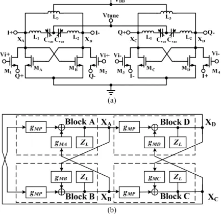
Fig. 1. (a) Schematic of parallel-coupled QILFD and (b) its equivalent block diagram.
4. Circuit Design
Figure 1(a) shows the proposed dual-resonance QILFD composed two differential dual-resonance VCO circuits [7]. One VCO is composed of a cross-coupled pair (MA, MB), transformer (L1, L2), varactors Cvar and a center-tapped inductor L3. The nMOSFETs (MA, MB) generate negative resistance to compensate for the resistive LC-tank loss. A series-resonator consists of transformer (L1, L2), and accumulation-mode varactor Cvar. The parallel-tuned resonator is composed of inductor L3 and the parasitic capacitor due to active transistors. The second VCO has the same device components as the first VCO. In traditional single-resonance QILFDs [9, 10] 4 common source amplifiers are used to couple two differential ILFDs to form the QILFD and two additional injection MOSFETs are used to couple the injection signal into the resonators. In the present dual-resonance QILFD, the transistors M1-M4 are used as the common gate transistor amplifiers with the LC resonators as the loads and QILFD outputs as the inputs of amplifiers, and the gates of M1-M4 are dc biased at VINJ for optimal locking range. The four quad transistors M1-M4 are arranged in a ring configuration and the gates of the common source amplifiers can be used to couple injection signal into the LC resonators and the injection signal is ac applied to the gates of M1-M4. Without the injection signal applied to the gates of the quad MOSFETs, the whole circuit is a dual-band quadrature VCO (QVCO) [8], which can oscillate by ensuring the differential negative resistance to overcome the loss due to the dual-resonance tank and coupling transistors. Figure 1(b) shows the block diagram of the proposed parallel-coupled QILFD to show the operation of the circuit, the QILFD can be modeled by 4 identical blocks. Xi in Fig. 1 represent the node voltages, and the subscript i is given by A, B, C or D. gMi stands for the transconductance of transistors Mi. gMP stands for gMn+gMb where gMn and gMb represents the transconductance and body trans-conductance of transistors M1-M4, respectively. The output voltage Xi is fed back through the coupling transistors M1-M4 and to be converted to the output drain current. The impedance ZL is due to the dual-resonance LC resonator and the parasitic resistance of active transistors. The decrease of channel output conductance decreases the
quality factor of the whole resonator. In Fig. 1(b), the ac voltages at the QILFD core outputs are denoted as XA, XB, XC and XD respectively. The ac voltage XA can be expressed as:
XAXBmXCgMAZL (1) where m= gMP/gMi. Because of XA=-XB, (1) can be modified as:
XA XAmXCgMAZL (2) Similarly, the ac voltage XC can be expressed as:
XC XCmXAgMCZL (3)
When both oscillators synchronize to a single oscillation frequency, the circuit is symmetrical, gMA and gMC
are identical to gM, and the coupling coefficients are the same, from (2) and (3), we can get XA = jXC, and XB = jXD. The oscillator produces quadrature outputs. The oscillation frequency ω can be found from (2) or (3) and is expressed as:
(1 jm)gM ZL(j)1 (4)
This equation indicates that the oscillation frequency of the dual-resonance QILFD is also modified by the coupling devices.
The proposed QILFD has potential for low power operation. First of all, the QILFD uses the common-gate amplifiers as the coupling devices, which do not consume dc power because the dc drain-source voltage is zero. Despite the dc drain-source voltage is zero, the ac drain-source voltage is not zero, and the ac voltage can be used to amplify the signal while a signal is applied to the gate. In the QILFDs [9, 10] using the parallel-coupled devices and series-coupled devices, the power is increased because the dc current or the dc voltage is increased. Secondly, the output voltage in the n-core VCO shown in Fig. 1(a) can switch above the supply voltage so that a low supply voltage can be used. Thirdly, nanometer nMOSFETs with the threshold voltage of 0.48V are used, and they have higher transconductance gain as compared with the 0.18 μm MOSFETs due to shorter channel length.
A dual-band QILFD can also be formed by another way. Firstly a direct injection MOSFET across the resonator is used to form a differential ILFD and then two identical ILFDs are coupled via an active or passive coupling network. In the direct injection MOSFET, the source voltage and drain voltage are phase-shifted by 180º, and the output current of the injection MOSFET doesn’t have the information of quadrature phase. In the used injection method, the source voltage and drain voltage of injection MOSFET are phase-shifted by 90º, so the output current of the quad mixer contains the information of the injection signal and fundamental oscillation signal including strength and phase. However, the injection efficiency of the direct-injection method is higher because the net drain-source swing of the mixer is larger. Both the QILFDs can operate at low power because of only one level of cross-coupled transistors is used.
5. Measurement and Discussion
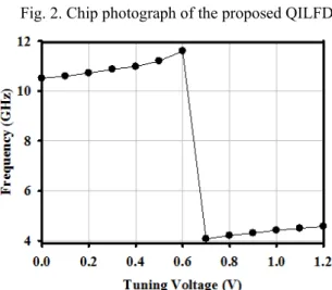
Figure 2 shows the micrograph of the TSMC 90 nm QILFD with a chip area of 0.973 × 0.933 mm2 including the pads. To measure the locking range and phase noise performance of the QILFD, the Agilent 83752B and E8257D signal generators have been used with the Agilent E4407B spectrum analyzer. Figure 3 shows the high-frequency band output frequency as the control voltage Vtune is tuned from 0 V to 1.2 V. When
Fig. 2. Chip photograph of the proposed QILFD.
Fig. 3. Measured tuning range. VDD = 0.5 V, and VINJ = 0.7 V.
Fig. 4. Measured locking range of the QILFD. VINJ = 0.7 V and VDD = 0.5 V.
Vtune increases from 0.6 V to 0.7 V, the oscillator switches from its parallel resonance frequency pe to series resonance frequency se. The oscillator is tunable from 10.5 GHz to 11.6 GHz for the high-frequency band and from 4.1 GHz to 4.6 GHz for the low-frequency band at the supply voltage of 0.5 V. With the supply voltage of VDD = 0.5 V, the current and power consumption of the core QILFD are 4.62 mA and 2.31 mW, respectively. The high-band tuning range is due to the parallel-tuned resonator where the transformer (L1, L2) plays a minor role in affecting the oscillation frequency. The voltage swing Vs at the common node of (L1, L2) and Cvar is smaller than the voltage swing Vo at the QILFD output. The low-band tuning range is due to the whole resonator and the transformer (L1, L2) plays a major role in affecting the oscillation frequency. The voltage swing Vsis larger than Vo at the QILFD output.
The transistors in the quad are used as linear mixers, and common-source amplifiers. The gate of injection MOSFET is biased at a level higher than the source and drain voltage so that the injection MOSFET can be used as a linear mixer. The transistor quad is designed to provide the required locking range and quadrature phase outputs. Figure 4 shows the measured relationship between input sensitivity and operating frequency
(a) (b)
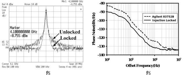
Fig. 5. (a) Measured spectra and (b) phase noises of the injection-reference and the locked high-band QILFD. VDD = 0.5 V, Vtune = 0.2 V, VINJ = 0.7 V.
Offset Frequency(Hz)
104 105 106 107
Phase Noise(dBc/Hz)
-140 -130 -120 -110 -100 -90 -80
Agilent 83752B Injection Locked
(a) (b)
Fig. 6. (a) Measured spectra and (b) phase noises of the injection-reference and the locked QILFD. VDD = 0.5 V, Vtune = 0.7 V, VINJ = 0.7 V.
of the divide-by-2 QILFD as the control voltage was tuned from 0 V to 1.2 V. When the tuning voltage is varied, the locking range curves shift because of the oscillation frequency varies. At Vtune = 0 V, the high-frequency band locking range is from 19.8 GHz to 23.9 GHz at the input power of 0 dBm. At Vtune = 1.2 V, the low-frequency locking range is from 7.6 GHz to 10.1 GHz at the input power of 0 dBm. The overall operation range is extended by the oscillation frequency tuning.
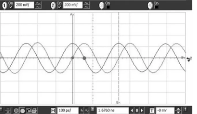
Figure 5 shows the measured spectra and phase noises of the injection signal and injection-locked oscillator outputs in the high-frequency band. When the signal is injected, at 1 MHz frequency offset the phase noise of the ILFD is -132.10 dBc/Hz, while the phase noise of the injection-reference is -131.38 dBc/Hz. Figure 6 shows the measured spectra and phase noises of the injection signal and injection-locked oscillator outputs in the low-frequency band. When the signal is injected, at 1 MHz frequency offset the phase noise of the ILFD is -131.75 dBc/Hz, while the phase noise of the injection-reference is -124.12 dBc/Hz. At low offset frequency, the phase noise of the locked ILFD is smaller than the injection signal by about 7.63 dB. Figure 7 shows the measured time-domain output waveforms of two dual-band quadrature ILFD output buffers by using the Agilent 54855A Infiniium oscilloscope. The average output phase error is 0.5° Table I summarizes the performance comparison of QILFDs.
Fig. 7. Measured low-band output waveforms of the I and Q channels. Vdd = 0.5V, Vtune = 0.45 V, VINJ=0.7V and fosc = 3.996 GHz.
Table I Performance Comparison of Divide-by-2 QILFDs.
6. Conclusion
This work proposes a novel low power LC-tank divide-by-2 dual-band QILFD which consists of two n-core dual resonance VCOs coupled by a transistor quad which also serves as an injection device. The transistors in the quad in conjunction with the dual-resonance resonator form the coupling network with common gate amplifiers. The QILFD has been successfully implemented in the TSMC 90nm CMOS process and has wide-band operation. locking ranges from 7 to 10.1 GHz for the low-frequency band and from 19.8 to 24.6 GHz for the high-frequency band. This dual-resonance QILFD provides enough output power and locking range, and has potential for RF application.
References
[1] Y.-H. Chuang, S.-H. Lee, R.-H. Yen, S.-L. Jang, J.-F. Lee, and M.-H. Juang,” A wide locking range and low voltage CMOS direct injection-locked frequency divider,” IEEE Microw. Wireless Compon. Lett., vol. 16, no. 5, pp. 299-301, May 2006.
[2] H. R. Rategh and T. H. Lee, “Superharmonic injection-locked frequency dividers,” IEEE J. Solid-State Circuits, vol. 34, no. 6, pp. 813–821, June 1999.
[3] A. Mazzanti, P. Uggetti, and F. Svelto, “Analysis and design of injection locked LC dividers for quadrature generation,” IEEE J.
Solid State Circuits, vol. 39, no. 9, pp. 1425–1433, Sep. 2004.
[4] A. Mazzanti and F. Svelto, “A 1.8-GHz injection-locked quadrature CMOS VCO with low phase noise and high phase accuracy,” IEEE Trans. Circuits Syst., vol. 53, no. 3, pp. 554–560, Mar. 2006.
[5] S.-L. Jang, Y.-H. Chung, S.-H. Lee, L.-R. Chi, and J.-F. Lee,” An integrated 5/2.5GHz direct-injection locked quadrature LC VCO ,” IEEE Microw. Wireless Compon. Lett., vol. 17, no. 2, pp. 142-144, Feb. 2007.
[6] S.-L. Jang, Y.-H. Chuang, S.-H. Lee and Y.-H. Chiang,” A current reused CMOS quadrature injection locked frequency divider ,” Microwave and Optical Tech. Lett., vol. 49, no. 8, pp. 1804-1806, Aug. 2007.
[7] S.-L. Jang, Y.-K. Wu, C.-C. Liu and J.-F. Huang, ” A Dual-band CMOS voltage-controlled oscillator implemented with dual-resonance LC tank,” IEEE Microw. Wireless Compon. Lett., vol. 19, No. 12, pp.816-818, Dec. 2009.
[8] Q. Gu, Z. Xu, D. Huang, T. LaRocca, N. Y. Wang, W. Hant, and M. C. F. Chang, “A low power V-Band CMOS frequency divider with wide locking range and accurate quadrature output phases,” IEEE J. Solid-State Circuits, vol. 43, no. 4, pp.
991–998, Apr. 2008.
[9] S.-L. Jang, Y.-H. Chuang, S.-H. Lee and Y.-H., Chiang,” A current reused CMOS quadrature injection locked frequency divider ,” Microwave and Optical Technology Lett., pp.1804-1806, Aug. 2007.
[10] S.-L. Jang, S.-C. Wu, C.-F. Lee and M.-H. Juang ,” CMOS top-series coupling quadrature injection-locked frequency divider,”
Microwave and Optical Technology Lett., pp. 2554-2557, Oct. 2008.
[11] S.-L. Jang, C.-W. Chang, S.-C. Wu, C.-F. Lee, L.-Y. Tsai,and J.-F. Huang, ”Quadrature Hartley VCO and injection-locked frequency divider,” IEICE Trans. Electron., Vol.E91-C, pp1371.-1374,Aug. 2008.
[12] S.-L. Jang, C.-C. Liu, and J.-F. Huang ” A wide locking range quadrature injection locked frequency divider with tunable active inductor,” IEICE Trans. Electron., vol. E91-C, no. 3, pp. 373-377, Mar. 2008.
Pin (dBm) /VDD(V)
Pdiss.
(mW)
Operation Range (GHz) (%)
[11] 0/1.5 26.55 3.99~5.19 (36.6%) [12] 0/1.8 22.86 1.37~7.38 (137%) This 0/0.5 2.31 7.0~10.1 (36.26%)L-band
19.8~ 24.6 (21.62%)H-band
國科會補助專題研究計畫成果報告自評表
請就研究內容與原計畫相符程度、達成預期目標情況、研究成果之學術或應用價 值(簡要敘述成果所代表之意義、價值、影響或進一步發展之可能性)、是否適 合在學術期刊發表或申請專利、主要發現或其他有關價值等,作一綜合評估。
1. 請就研究內容與原計畫相符程度、達成預期目標情況作一綜合評估
■
達成目標□ 未達成目標(請說明,以 100 字為限)
□ 實驗失敗
□ 因故實驗中斷
□ 其他原因
2. 研究成果在學術期刊發表或申請專利等情形:
論文:■已發表 □未發表之文稿 □撰寫中 □無 專利:□已獲得 □申請中 □無
技轉:□已技轉 □洽談中 □無
1. Sheng-Lyang Jang, Li-Te Chou, Jhin-Fang Huang, Chia-Wei Chang, ” A Dual-Band Dual-Resonance Quadrature Injection-Locked Frequency Divider,” IEICE Trans. on Electron., Vol.E94-C,No.8,pp.1336-1339, Aug. 2011.
2. Sheng-Lyang Jang, Chia-Wei Chang, Chong-Wei Huang, and Ching-Wen Hsue, ” A Dual-Resonance Injection-Locked Frequency Doubler in 0.18 μm CMOS Technology,” Microwave and Optical Technology Lett., pp.193-196, Jan., 2012.
3. Chia-Wei Chang, Sheng-Lyang Jang, Chong-Wei Huang, and Chih-Chieh Shih, " Dual-resonance LC-tank frequency divider implemented with switched varactor bias,” IEEE Int. VLSI- DAT, 2011. pp.1 – 4.
3. 請依學術成就、技術創新、社會影響等方面,評估研究成果之學術或應用價 值(簡要敘述成果所代表之意義、價值、影響或進一步發展之可能性)(以 500 字為限
本計畫主要目的是使用雙共振腔來設計超寬鎖頻範圍除頻器,除頻器主要應 用於鎖相迴路(PLL)內,運用我們設計的雙共振腔架構,可以讓電路工作在兩個頻 帶或是相鄰的兩個頻帶,加上我們設計的寬鎖定範圍注入鎖定除頻架構,可以設 計出雙頻帶或超寬頻工作範圍的除頻器。本次計畫設計電路擁有寬注入鎖定除頻 範圍、低功耗、小面積等特色。
研究項目應用範圍:應用於鎖相迴路系統,應用於高頻系統晶片,低功耗,超 寬工作頻帶。
主要創新技術:超寬除頻範圍注入鎖定除頻器,使用雙共振腔架構讓電路工 作在兩個頻帶或是相鄰的兩個頻帶來增強除頻範圍,可延伸應用開發除三除四或 更高除頻模數除頻器。
附件二
國科會補助專題研究計畫項下出席國際學術會議心得報告
日期: 年 月 日
一、參加會議經過
本會議的名稱為International Electron Devices and Materials Symposium 2011,由於本次投稿被接受 為oral presentation,因此學生和指導教授張勝良教授早上即驅車前往台北參加會議,報告的過程順利圓 滿。
二、與會心得
參與國際會議不外乎瞭解目前最新的發展情況、具潛力的方向以及語言上的表達訓練。在會議上 與會來賓和演說者亦相互分享彼此的研究內容與經驗。對於他們勇於發問的精神感到十分欽佩,反覆 思索後發覺,對問題的敏感度以及分析能力是現階段急需養成的,愈是透徹了解問題的原因與解決的 方法才能減少錯誤的嘗試及增加投入研究的信心。
三、考察參觀活動(無是項活動者略) 四、建議
暫無。
五、攜回資料名稱及內容
會議流程、會議論文、大會光碟等資料。
六、其他 暫無。
計畫編號 NSC 100-2221-E-011-094-
計畫名稱
前瞻性毫微米金氧半電晶體雙共振注入鎖定除頻器特性研究
出國人員
姓名 張珈瑋 服務機構 及職稱
國立台灣科技大學電子工程系(所)
會議時間
2011 年 11 月 17 日 至
2011 年 11 月 18 日
會議地點 台灣台北
會議名稱
(中文)2011 國際電子元件與材料研討會
(英文)International Electron Devices and Materials Symposium 2011 發表論文
題目
1. Low-Power Wide Operation Range 0.35 μm SiGe HBT Injection Locked Frequency Divider 2. A Low Power Injection Locked Frequency Divider Using the Shunt Peaking Transformer 附件四
國科會補助計畫衍生研發成果推廣資料表
日期:2012/08/08
國科會補助計畫
計畫名稱: 前瞻性毫微米金氧半電晶體雙共振注入鎖定除頻器特性研究 計畫主持人: 張勝良
計畫編號: 100-2221-E-011-094- 學門領域: 積體電路及系統設計
無研發成果推廣資料
100 年度專題研究計畫研究成果彙整表
計畫主持人:張勝良 計畫編號:100-2221-E-011-094- 計畫名稱:前瞻性毫微米金氧半電晶體雙共振注入鎖定除頻器特性研究
量化
成果項目 實際已達成
數(被接受 或已發表)
預期總達成 數(含實際已
達成數)
本計畫實 際貢獻百
分比
單位
備 註 ( 質 化 說 明:如 數 個 計 畫 共 同 成 果、成 果 列 為 該 期 刊 之 封 面 故 事 ...
等)
期刊論文 0 0 100%
研究報告/技術報告 0 0 100%
研討會論文 4 4 100%
論文著作 篇
專書 0 0 100%
申請中件數 0 0 100%
專利 已獲得件數 0 0 100% 件
件數 0 0 100% 件
技術移轉
權利金 0 0 100% 千元
碩士生 3 3 100%
博士生 1 1 100%
博士後研究員 0 0 100%
國內
參與計畫人力
(本國籍)
專任助理 0 0 100%
人次
期刊論文 21 21 100%
研究報告/技術報告 0 0 100%
研討會論文 2 2 100%
論文著作 篇
專書 0 0 100% 章/本
申請中件數 0 0 100%
專利 已獲得件數 0 0 100% 件
件數 0 0 100% 件
技術移轉
權利金 0 0 100% 千元
碩士生 3 3 100%
博士生 1 1 100%
博士後研究員 0 0 100%
國外
參與計畫人力
(外國籍)
專任助理 0 0 100%
人次
其他成果
(無法以量化表達之成
果如辦理學術活動、獲 得獎項、重要國際合 作、研究成果國際影響 力及其他協助產業技 術發展之具體效益事 項等,請以文字敘述填 列。)
無
成果項目 量化 名稱或內容性質簡述
測驗工具(含質性與量性) 0
課程/模組 0
電腦及網路系統或工具 0
教材 0
舉辦之活動/競賽 0
研討會/工作坊 0
電子報、網站 0
科 教 處 計 畫 加 填 項
目 計畫成果推廣之參與(閱聽)人數 0
國科會補助專題研究計畫成果報告自評表
請就研究內容與原計畫相符程度、達成預期目標情況、研究成果之學術或應用價 值(簡要敘述成果所代表之意義、價值、影響或進一步發展之可能性)、是否適 合在學術期刊發表或申請專利、主要發現或其他有關價值等,作一綜合評估。
1. 請就研究內容與原計畫相符程度、達成預期目標情況作一綜合評估
■達成目標
□未達成目標(請說明,以 100 字為限)
□實驗失敗
□因故實驗中斷
□其他原因 說明:
2. 研究成果在學術期刊發表或申請專利等情形:
論文:■已發表 □未發表之文稿 □撰寫中 □無 專利:□已獲得 □申請中 ■無
技轉:□已技轉 □洽談中 ■無 其他:(以 100 字為限)
3. 請依學術成就、技術創新、社會影響等方面,評估研究成果之學術或應用價 值(簡要敘述成果所代表之意義、價值、影響或進一步發展之可能性)(以 500 字為限)
本計畫主要目的是使用雙共振腔來設計超寬鎖頻範圍除頻器,除頻器主要應用於鎖相迴路 (PLL)內,運用我們設計的雙共振腔架構,可以讓電路工作在兩個頻帶或是相鄰的兩個頻 帶,加上我們設計的寬鎖定範圍注入鎖定除頻架構,可以設計出雙頻帶或超寬頻工作範圍 的除頻器。本次計畫設計電路擁有寬注入鎖定除頻範圍、低功耗、小面積等特色。可延伸 應用開發除三除四或更高除頻模數除頻器。